Abstract
Ultrathin manganite films are widely used as active electrodes in organic spintronic devices. In this study, a scanning tunnelling microscopy (STM) investigation with atomic resolution revealed previously unknown surface features consisting of small non-stoichiometric islands. Based upon this evidence, a new mechanism for the growth of these complex materials is proposed. It is suggested that the non-stoichiometric islands result from nucleation centres that are below the critical threshold size required for stoichiometric crystalline growth. These islands represent a kinetic intermediate of single-layer growth regardless of the film thickness, and should be considered and possibly controlled in manganite thin-film applications.
Complex magnetic oxides display intriguing bulk and surface properties that make these materials very promising candidates for spintronics and other magnetic applications1. However, controlling material stoichiometry and homogeneity is extremely difficult, especially at the nanoscale. Therefore, the characterisation of various nanoscale features that may affect certain material parameters is important for enabling the manufacture of robust and reproducible devices.
Scanning tunnelling microscopy (STM) and spectroscopy (STS) are powerful tools for characterising the nanoscale properties of surface electronic states, acquiring local information without significant lateral averaging2,3.
Achieving an atomic-scale resolution in the STM imaging of manganites is an arduous task due to both the non-ideal atomically smooth surface topology and the high charge delocalisation4,5,6. The information obtained to date is sparse and does not provide a general or quantitative understanding of manganite surface features. To try to overcome these deficits, we investigated ultrathin films of the prototypical manganite La0.7Sr0.3MnO3 (LSMO). Our investigation of this material was particularly motivated by its relevance to organic spintronics devices7,8,9. Thicknesses of just 2–3 nm ensure sufficient damping of the system metallicity and simultaneously decrease the number of statistical defects, which increases with thickness. Investigating such systems allowed us to unambiguously image the atomic structures of ultrathin films of LSMO. Our results provide new insights into the surface properties of manganites as well as suggesting a new mechanism for the film growth of such complex materials. We detected a minority phase dispersed on a stoichiometric crystalline matrix; this phase consisted of small (less than tens of nm2) non-stoichiometric islands that represent a kinetic intermediate of single-layer growth. We propose a phenomenological mechanism for the formation of such defects suggesting that they are characteristic features of all manganite films, although the detection of these defects is mainly obstructed at greater thicknesses.
Results
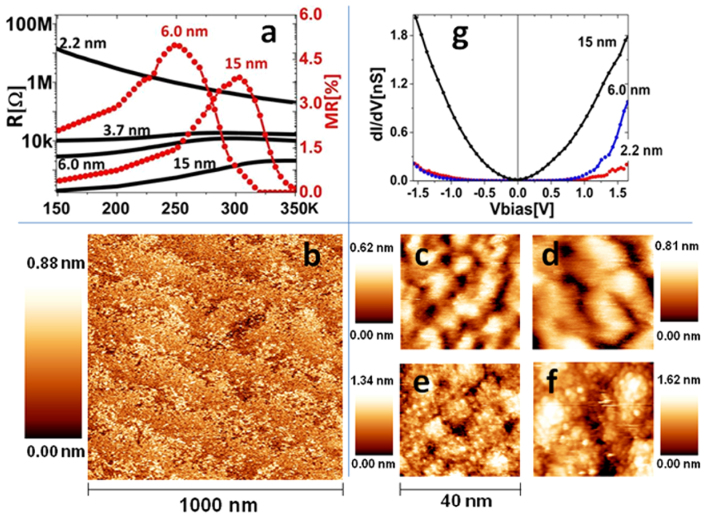
Fig. 1 summarises certain relevant properties of manganite ultrathin films. Resistance (R) along with magnetoresistance (MR) characterisations provide a comprehensive description of the electric and magnetic properties of these materials and reveal the characteristic metal-insulator transition (MIT). The R vs. temperature (T) dependence and low-field MR of the 4 samples described in Table 1 are shown in Fig. 1(a). The 15-nm-thick sample had no transition to a semiconducting-like behaviour in the R(T) curve within the temperature range investigated, and the Curie temperature of this sample as determined from the MR(T) curve was nearly 320 K. Such behaviour is typical of LSMO films of this thickness, making this sample a benchmark10. The MIT temperature (TMI) and the Curie temperature (TC) shifted to approximately 300 K for the 6-nm-thick film and 280 K for the 3.7-nm sample. Finally, the 2.2-nm-thick sample showed neither a metallic phase nor MR. This reduction in magnetism and metallicity with decreasing film thickness is qualitatively and quantitatively similar to results reported recently for manganite thin films of the highest quality, which exhibited thickness variations of approximately 1–2 nm between different groups and deposition methods10,11,12,13,14.
Figure 1.
(a) Resistance (R) (black curves) and magnetoresistance (MR) (red curves) versus temperature (T) for four samples of different thicknesses across the metal-insulator transition (MIT): 2.2 nm, 3.7 nm, 6 nm and 15 nm. (b) 1000 × 1000 nm2 topographic image of the 2.2-nm-thick sample (Vbias = 1.2 V, I = 0.06 nA). (c–f) 40 × 40 nm2 micrographs of the four sample thicknesses, respectively c) 2.2 nm, d) 3.7 nm, e) 6 nm and f) 15 nm. (Vbias = 1.2–0.6 V, I = 0.06–0.12 nA, depending on the sample thickness and local tunnelling conditions). (g) Room temperature differential tunnel conductivity curves measured on the three indicated samples.
Table 1. Films thickness vs transport properties and STM findings.
| Nominal Thickness [nm] | Measured Thickness [nm] | M-I Transition | MR @ RT | Atomic Resolution @ RT |
|---|---|---|---|---|
| 2 | (2.2 ± 0.1)a | NO | NO | YES |
| 4 | (3.7 ± 0.1)a | <RT | NO | YES |
| 6 | (6 ± 1)b | RT | YES | NO |
| 13 | (15 ± 2)b | >RT | YES | NO |
| 25 | (20 ± 2)b | >RT | YES | NO |
| 70 | (75 ± 5)b | >RT | YES | NO |
aby direct XRR measurement;
bby profilometer-based calibration.
The STM characterisations performed at room temperature (RT) revealed no large surface defects (such as outgrowths) for areas as large as 2 × 2 μm2. In Fig. 1(b), a 1000 × 1000 nm2 topographic region of the thinnest sample displays growth terraces 100–200 nm wide characterised by approximately 0.4-nm height steps (approximately one LSMO unit cell (u.c.)), in good agreement with previous STM reports and the layer-by-layer growth mechanism expected for LSMO films with small thicknesses12,15. At this scale, the measured root mean square (RMS) roughness was between 0.5 and 1.0 u.c. and gradually increased with increasing film thickness up to 2.0–2.5 u.c. for the 15-nm-thick sample. The evolution of the surface morphology (Fig. 1(c–f)) for the investigated thicknesses can be described in relation to the frequently observed grain-like structures6,16, in which the topological complexity increased along with the thickness.
The surface tunnelling spectroscopy is shown in Fig 1(g), where the dI/dV curves for three different thicknesses are plotted. All the spectra were averaged and acquired at the same tunnel resistance (see the Methods section). The curves illustrate the evolution of the sample from a paramagnetic insulating (PI) to a ferromagnetic metallic (FM) phase, which is accompanied by a consistent increase in the metallicity, in agreement with the R(T) curves in Fig. 1(a). We also observed no significant correlation between the topographic and spectroscopic features of the films at room temperature, consistent with previous reports on LSMO17,18,19. Finally, the correspondence between the STS and the transport measurements confirmed that the physical properties of the local microscopic probes directly influenced the macroscopic device parameters.
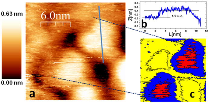
Further investigation of the grain-like structures revealed interesting details, especially for the two samples located in the insulating phase before the MIT. Fig. 2(a) displays a 20 × 20 nm2 STM micrograph of the 2.2-nm-thick sample, in which regions spatially confined within one or a few tens of nm2 stack approximately 0.2 nm (one-half of the u.c.) above the surrounding “background”, as shown by the line profile in Fig. 2(b). Such regions were characteristic of the entire LSMO surface, and the typical geometry of these areas is depicted in Fig. 2(c), wherein the 0.2-nm-step height above the grain is indicated by different colours. We observed similar half-cell terminated regions on both the 2.2-nm and 3.7-nm samples, while the observation of such regions on the 6-, 15- and 75-nm-thick samples was prevented by slight roughness increases.
Figure 2.
(a) 20 × 20 nm2 STM micrograph of the 2.2-nm-thick sample showing a detail of the grain-like surface (Vbias = 1.2 V, I = 0.06 nA). (b) Line profile over the grain surface, indicating a step height of 0.2 nm. (c) Magnification of the image in (a), where the red to blue transition corresponds to a step height of 0.2 nm along the z-scale, revealing a defect island.
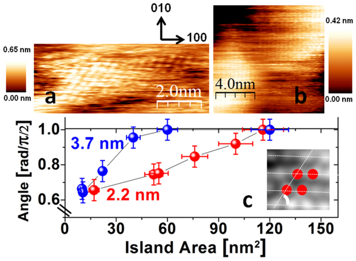
Further magnification enabled the observation of the half-cell stacks at an atomic resolution, the primary result of this study. Fig. 3(a–b) shows atomically resolved regions of the 2.2–nm- and 3.7-nm-thick samples. Fig. 3(a) covers an area of a few tens of nm2 and reveals a region of ordered atoms characterised by sizeable angular distortion with respect to the expected square perovskite-like cell. A number of similar atomic patterns were detected on the same sample within distances of less than hundreds of nm. Among these, the atomically resolved regions characterised by larger areas resulted in a smaller distortion (Fig. 3(b)). This trend (the larger the area, the smaller the distortion) was confirmed on both of the thin samples. An analysis of this phenomenon is presented in Fig. 3(c); the inset indicates the method used to estimate the characteristic angle of the pseudo-cells. It is evident that the distortions (and hence the deviation from the standard structure) tend to disappear as the size of the island increases. This result is opposite to the behaviour expected from surface reconstruction effects, wherein larger groups of atoms result in stronger stabilisation of the distorted reconstructed surface20. Moreover, the distortion magnitude observed in our films was thickness dependent. Fig. 3(c) indicates that the changes in the angle of distortion as a function of island area are clearly different for the 2.2-nm- and 3.7-nm-thick samples.
Figure 3.
(a) 5 × 10 nm2 STM micrograph with a single defect island featuring an angular deviation from the expected perovskite-like square shape (Vbias = 1.2 V, I = 0.06 nA). (b) 11 × 11 nm2 image featuring a square LSMO cell (Vbias = 1.2 V, I = 0.06 nA). (c) Plot of the angle vs. island area for the two thinnest samples; the inset indicates how we estimated the angle starting from a given image (the sample image is an offline zoom of an atomically resolved image of the 3.7-nm sample).
Discussion
The data presented above reveal previously unknown and unpredicted features of the growth of LSMO films. In discussing these results, we should stress that LSMO represents a stoichiometrically complex compound. Considering the La/Sr molar ratio in the composition of a La(0.7)Sr(0.3)MnO3 film, it is evident that a minimum of 7 + 3 = 10 u.c. along two perpendicular axes in the (001) plane are necessary to achieve the stoichiometric composition for a layer grown on top of the already established stoichiometric LSMO underlayer. This defines an area of at least 100 u.c. or approximately 15 nm2 for a cell parameter of a = 0.3873 nm (see Methods).
Furthermore, the La/Sr ratio and distribution typically deviate from the perfect value (7/3) due to composition fluctuations in the atomic flux arising from the target and due to the different La and Sr adatom mobilities21. Although such deviations have never been accurately quantified for thin manganite films, it is evident that the proposed estimation of “7 + 3 u.c.” fails even for weak deviations. Indeed, a composition of La(0.71)Sr(0.29)MnO3 would require a set of 71 + 29 u.c. to guarantee the stoichiometry. Therefore, the size of the island necessary to establish a perovskite structure with the required composition/stoichiometry would be increased by one order of magnitude.
These considerations led us to propose a critical island size. The crude estimation proposed above suggests an upper level boundary, such that a critical surface area SC ≤ 150 nm2 (1000 cells) should be able to stabilise the perovskite phase with the stoichiometry corresponding to the previously formed layers. This order-of-magnitude estimation agrees well with Fig. 3(c), wherein the distorted phase is observed in areas less than 120 nm2.
Within this framework, adatom islands exceeding the SC evolve by establishing a stoichiometric perovskite structure, while smaller islands (S < SC) are expected to develop temporary 2D metastable structures with all atoms, i.e., La, Sr, Mn and O, lying in the same plane and ordered in a distorted lattice, minimising the system energy with respect to the random orientation. We anticipate that this behaviour will be characteristic of any multi-composite material grown via Frank-van der Merwe 2D growth22, whereas for a step-flow growth, the stoichiometric defects would be confined near the frozen step edge.
This model provides a straightforward physical explanation of the detected atomically resolved regions. The interruption of the film deposition and the subsequent freezing of the structure will obviously result in a random number of adatoms that are unable to produce fully complete layers. We therefore propose that the regions observed at an atomic resolution correspond to defects formed by islands with areas that are below the critical area (S < SC).
The role of defects in the atomic resolution of manganites has already been widely emphasized: in manganites, despite the low density of charge carriers (~1022 cm−3) compared to metals, charge screening is a strong limiting factor in the maximum lateral resolution achievable by STM4,5,6. Static distortions identified as trapped polarons have been proposed as a necessary requisite to achieve atomic resolution in layered manganite La2−2xSr1+2xMn2O74 and in La0.75Ca0.25MnO35 thin films.
Moreover, atomically resolved images have been obtained only from the PI phase of manganites4,23,24,25, similar to our set of samples (see Table 1). The semiconducting behaviour of ultrathin LSMO films below the MIT favours the resolution of individual atoms by STM because this behaviour is related to the presence of localised states on the surface that enhance spatial variations in the tunnelling current between the surface and the tip.
The thickness dependence shown in Fig. 3(c) and the lack of atomically resolved islands in the thicker samples can be explained based upon the proposed growth model. In the 2D-island growth mode, the film roughness is expected to increase with increasing film thickness due to residual non-coalesced small islands22. The higher the density of the surface defects, the higher the density of the nucleation centres that lead to small-area islands22. We expect that 6- and 15-nm-thick samples would feature a large number of a few nm2-sized non-stoichiometric islands that cannot be resolved internally via STM due to both the higher system metallicity and the higher surface roughness. Indeed, for the thicker samples, no atomically resolved regions were detected, although 0.2 nm (one-half u.c.) steps were widely present on the film surfaces.
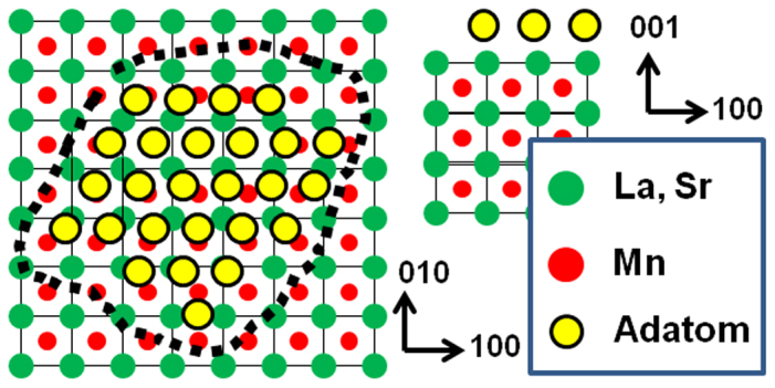
Increasing the film thickness augments the metallicity of the manganite films, enhancing the screening effects in the STM visualisation (see above). This further decreases the ability of STM to resolve images with an atomic scale resolution. Our observation sheds new light on the mechanism of perovskite film growth by examining the monolayer growth process. (The cell-by-cell growth models based on RHEED oscillations are mere approximations). Fig. 4 illustrates the proposed model of the distorted, atomically resolved islands. The observed 2D non-stoichiometric islands represent strong potential defects for both charge and spin injection from the manganite electrodes. Understanding and controlling these islands is therefore of great importance. A deeper understanding of these effects will require the use of complementary surface techniques and considerable modelling efforts. However, we can rule out some possible competing mechanisms like surface reconstruction (see above) or the effects caused by the topological peculiarity of the surface, such as ion-reduced coordination, not able to generate half u.c. steps.
Figure 4. Schematisation of the “freezing” adatoms - forming a defect island - upon the “perfect” and mono-terminated LSMO surface.

In conclusion, ultrathin LSMO films grown epitaxially on SrTiO3 substrates were visualised with unprecedented size resolution. We emphasise the role played by inhomogeneities in the uppermost layer formation. Our findings revealed a separate surface phase associated with non-stoichiometrical defects in the uppermost film layer and promote significant revisions to the LSMO film growth mechanism.
Methods
Film deposition
High quality colossal magnetoresistance manganite LSMO films were grown on cubic (a = 3.905Å) SrTiO3 (STO) substrates using the channel spark ablation (CSA) technique26,27,28. Bulk LSMO is rhombohedral at RT with a pseudocubic parameter a = 3.873Å and a distorted pseudo-cubic angle α = 90.26°29. The quality of the substrates was verified with atomic force microscopy (AFM) measurements, which revealed terraces of ~200 nm size, with step heights of approximately 0.4 nm, indicating a unique surface termination.
STM measurements
After the film deposition, the samples were transferred into the Omicron STM chamber under ultra high vacuum (UHV) conditions, and the surface was refreshed following the annealing procedures established by photo emission spectroscopy (PES) investigations21. The microscope was tip-biased and operated with PtIr tips. The images shown in Figs. 1, 2 and 3 were acquired at bias voltages of 0.5–1.2 V and tunnelling currents of 0.06–0.12 nA; the tunnelling conditions slightly varied depending on the sample thickness. Images were acquired over an area of 512 × 512 pixels in topographic mode and were unfiltered but levelled by a second-order line.
The dI/dV curves were acquired using the current imaging tunnelling spectroscopy technique, in which the tip is scanned in the constant current mode to maintain a constant distance from the sample. We recorded the I(V) curves on a grid of 1000 × 1000 spectra over an area of 1000 × 1000 nm2. Repeated measurements indicated that the I(V) curves, obtained as the average of tens to hundreds of curves, were representative of the region considered. The dI/dV characteristics in Fig. 1(g) were obtained by numerical differentiation and were acquired at the same reference values, namely 0.8 V and 60 pA.
Author Contributions
A.G. was responsible for the STM-STS and R(T) measurements; P.G. and I.B. were responsible for the sample preparation; M.P. and I.B. were responsible for the MR measurements, and S.M. was responsible for the XRR measurements. D.P. and F.B. wrote the manuscript, and V.D. was responsible for providing guidance for the experiments and the final editing of the paper.
Acknowledgments
The authors acknowledge the financial support from the FP7 project NMP3-LA-2010-246102 (IFOX), from NMP-2010-SMALL-4-263104 (HINTS) and from FP7 project NMP3-SL-2010-246073 (GRENADA).
References
- Bibes M. & Barthélémy A. Oxide spintronics. IEEE T. Electron. Dev. 54, 1003–1023 (2007). [Google Scholar]
- Tersoff J. Sample-dependent resolution in scanning tunneling microscopy. Phys. Rev. B 39, 1052–1057 (1989). [DOI] [PubMed] [Google Scholar]
- Koslowski B., Dietrich C., Tschetschetki A. & Ziemann P. Evaluation of scanning tunneling spectroscopy data: approaching a quantitative determination of the electronic density of states. Phys. Rev. B 75, 035421 (2007). [Google Scholar]
- RØnnow H. M., Renner Ch., Aeppli G., Kimura T. & Tokura Y. Polarons and confinement of electronic motion to two dimensions in a layered manganite. Nature (London) 440, 1025–1028 (2006). [DOI] [PubMed] [Google Scholar]
- Sudheendra L. et al. Direct imaging of lattice-strain-induced stripe phases in an optimally doped manganite film. Phys. Rev. B 75, 172407 (2007). [Google Scholar]
- Becker T. et al. Intrinsic inhomogeneities in manganite thin films investigated with scanning tunneling spectroscopy. Phys. Rev. Lett. 89, 237203 (2002). [DOI] [PubMed] [Google Scholar]
- Xiong Z. H., Di Wu Z., Vardeny & Shi Giant magnetoresistance in organic spin-valves. Nature 427, 821–824 (2004). [DOI] [PubMed] [Google Scholar]
- Bergenti I., Dediu V., Prezioso M. & Riminucci A. Organic spintronics. A. Phil. Trans. R. Soc. A 369, 3054–3068 (2011). [DOI] [PubMed] [Google Scholar]
- Prezioso M. et al. A single-device universal logic gate based on a magnetically enhanced memristor. Adv. Mater. 25, 534–538 (2013). [DOI] [PubMed] [Google Scholar]
- Huijben M. et al. Critical thickness and orbital ordering in ultrathin La0.7Sr0.3MnO3 films. Phys. Rev. B 78, 094413 (2008). [Google Scholar]
- Boschker H. et al. High-temperature magnetic insulating phase in ultrathin La0.67Sr0.33MnO3 films. Phys. Rev. Lett. 109, 157207 (2012). [DOI] [PubMed] [Google Scholar]
- Bongju Kim B. et al. Finite size effect and phase diagram of ultra-thin La0.7Sr0.3MnO3. Solid State Commun. 150, 598–601 (2010). [Google Scholar]
- Bergenti I. et al. Ultrathin manganite films grown by pulsed-plasma deposition. J. Magn. Magn. Mater. 310, e780–e782 (2007). [Google Scholar]
- Chopdekar,. Rajesh V., Elke,. Arenholz. & Suzuki Y. Orientation and thickness dependence of magnetization at the interfaces of highly spin-polarized manganite thin films. Phys. Rev. B 79, 104417 (2009). [Google Scholar]
- Postma, Ferry M. et al. Step-induced uniaxial magnetic anisotropy of thin films. Appl. Phys. Lett. 87, 242507 (2005). [Google Scholar]
- Singh U. R., Gupta A. K., Sheet G., Chandrasekhar V., Jang H. W. & Eom C. B. Pseudogap formation in the metallic state of La0.7Sr0.3MnO3 thin films. Appl. Phys. Lett. 93, 212503 (2008). [Google Scholar]
- Seiro S., Fasano Y., Maggio-Aprile I., Kuffer O. & Fischer Ø. Homogeneous spectroscopic properties in manganite films. J. Magn. Magn. Mater. 310, e243–e245 (2007). [Google Scholar]
- Seiro S. et al. Polaronic signature in the metallic phase of La0.7Ca0.3MnO3 films detected by scanning tunneling spectroscopy. Phys. Rev. B 77, 020407 (2008). [Google Scholar]
- Rana A. et al. Nanoscale modulation of electronic states across unit cell steps on the surface of an epitaxial colossal magnetoresistance manganite film. Appl. Phys. Lett. 96, 263108 (2010). [Google Scholar]
- Ercolessi F., Parrinello M. & Tosatti E. Au(100) reconstruction in the glue model. Surf. Sci. 177, 314–328 (1986). [Google Scholar]
- de Jong M. P., Dediu V. A., Taliani C. & Salaneck W. R. Electronic structure of La0.7Sr0.3MnO3 thin films for hybrid organic/inorganic spintronics applications. J. Appl. Phys. 94, 7292 (2003). [Google Scholar]
- Venables J. A., Spiller G. D. T. & Hanbucken M. Nucleation and growth of thin films. Rep. Prog. Phys. 47, 4 (1984). [Google Scholar]
- Rößler S. et al. Atomically resolved scanning tunneling microscopy on perovskite manganite single crystals. Appl. Phys. Lett. 96, 202512 (2010). [Google Scholar]
- Bryant B., Renner Ch., Tokunaga Y., Tokura Y. & Aeppli G. Imaging oxygen defects and their motion at a manganite surface. Nat. Commun. 2, 212 (2011). [DOI] [PubMed] [Google Scholar]
- Ma J. X., Gillaspie D. T., Plummer E. W. & Shen J. Visualization of localized holes in manganite thin films with atomic resolution. Phys. Rev. Lett. 95, 237210 (2005). [DOI] [PubMed] [Google Scholar]
- Dediu V. et al. Micro-raman and resistance measurements of epitaxial La0.7Sr0.3MnO3 films. Phys. Status Solidi B 215, 625–629 (1999). [Google Scholar]
- Graziosi P. et al. Conditions for the growth of smooth La0.7Sr0.3MnO3 thin films by pulsed electron ablation. Thin Solid Films 534, 83–89 (2013). [Google Scholar]
- Graziosi P. et al. Polaron framework to account for transport properties in metallic epitaxial manganite films. Phys. Rev. B (accepted May 2014). [Google Scholar]
- Trukhanov S. V., Troyanchuk I. O., Bobrikov I. A., Simkin V. G. & Balagurov A. M. Crystal structure phase separation in anion-deficient La0.70Sr0.30MnO3−δ manganite system. J. Surf. Invest.: X-Ray, Synchrotron Neutron Tech. 1, 705–710 (2007). [Google Scholar]


