Abstract
In order to effectively realize and control the critical coupling, a graphene-based hyperbolic metamaterial has been proposed to replace the absorbing thin film in the critically coupled resonance structure. Our calculations demonstrate that the critical coupling effect (near-perfect light absorption) can be achieved at the near-infrared wavelength by using this layered structure, while the critical coupling frequency can be tuned by varying the Fermi energy level of graphene sheets via electrostatic biasing. Moreover, we show that the critical coupling frequency can be tuned by changing the thickness of the dielectric or layer number of the graphene sheets in the unit cell of the graphene-dielectric HMM. The optimization performance has also been indicated, which may offer an opportunity towards the experimental designs of high efficient graphene based critical coupling devices.
Graphene has attracted intense scientific interests owing to its outstanding optical properties including the strong light-graphene interaction, the broadband and high-speed operation, giant nonlinear Kerr index (several orders of magnituede larger than conventional bulk media) and the controllable optical properties due to tunability of the charge carrier density by applying the bias voltage upon graphene1,2,3,4,5,6,7,8. Graphene also exhibits wavelength insensitive absorption in the visible- and near-infrared frequencies, which makes graphene a potential candidate as a building block for optical detectors and photovoltaic devices. However, absorption of the single-layer graphene remains very weak. Some methods had been proposed to enhance its absorption. Thongrattanasiri et al. demonstrated that 100% light absorption could occur if a single patterned sheet of doped graphene is designed instead9, Ferreira et al. reported that the absorption of graphene can reach up to 100% within Fabry-Pérot cavity sandwiched graphene structures10 or in graphene-metamaterial corrugated structures11, Nikitin et al. showed that graphene periodic antidot arrays could provide a strong electromagnetic absorption at both microwave and THz regions12, Nefedov et al. demonstrated that 100% light absorption could also be achieved in a graphene-based asymmetric hyperbolic metamaterial (HMM)13. In this paper, we show that near-perfect light absorption can be obtained by the critical coupling within graphene-based HMMs.
A critically coupled resonator (CCR) is a thin-film structure that can absorb nearly all of the incident electromagnetic radiation, leading to the null scattering. It was firstly reported by Tischler14,15, who experimentally demonstrated that a 5 nm thick film of high oscillator strength J-aggregated dye separated from a dielectric Bragg reflector by a dielectric spacer can absorb more than 97% of the incident light at the wavelength λ = 591 nm14. In the following, Gupta et al. replaced the polymer absorbing layer by a metal-dielectric composite film, and showed that the critical coupling (CC) frequency can be tuned by changing the volume fraction16. For a larger volume fraction, CC at two distinct frequencies can be obtained due to the strong coupling. Subsequently they extended their studies to oblique incidence for both the TE and TM polarizations17, Fabry-Perot cavity with metamaterial mirrors18, or layered media with Kerr nonlinearity19. However, a critically coupled system has limited flexibility for a given absorber material. The tunability of CC is intrinsically important for applications in optical devices. It is desired to tune CC in a fixed configuration or device by an external field. For this purpose, introducing graphene sheets into a CCR seems to be a good approach for achieving CC. Here, we replace the polymer absorbing layer or metal-dielectric composite film by the graphene-based HMMs20,21,22,23 composed of stacked graphene sheets separated by thin dielectric layers. It is found that such a graphene-based HMM can support controllable CC at a single wavelength.
Results
Graphene-based hyperbolic metamaterials
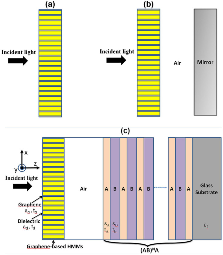
Our graphene-based HMM is representatively shown in Fig. 1(a). It is a graphene multilayer structure in which separations between graphene sheets are assumed to be filled with the dielectric. For the HMM in air, as shown in Fig. 1(a), the absorption is smaller than 50% generally and the perfect absorber cannot be constructed. In order to realize the perfect absorption, we try to construct a CCR by introducing a lossless metallic mirror to the back of the HMMs, as shown in Fig. 1(b). In the experiment, lossless metallic mirrors may be replaced by more realistic dielectric Bragg reflectors (DBRs). The designed CCR has been shown in Fig. 1(c), which is consisted by a graphene-based HMM separated from a DBR by a dielectric spacer. The graphene-based HMM acts as a thin absorbing film, which is created by alternating layers of graphene with the surface conductivity σ and slab thickness tg and conventional dielectric with a dielectric constant εd and slab thickness td. The period of the unit cell of the layered structure is t = td + tg. The graphene's surface conductivity can be calculated by adopting the Kubo formula24,25,26. Without considering the external magnetic field, the isotropic surface conductivity σ of graphene can be written as the sum of the intra-band σintra and the inter-band term σinter, where
 |
 |
where ω is the frequency of the incident light, EF is the Fermi energy, τ is the electron-phonon relaxation time, and T is a temperature in K. e,  and kB are the universal constants related to the electron charge, reduced Planck's constant, and Boltzmann constant, respectively. The Fermi energy
  can be electrically controlled by an applied gate voltage due to the strong dependence of the carrier density n2D on the gate voltage, where νF = 106 m/s is the Fermi velocity of electrons. Obviously, σ is highly dependent on the work frequency and Fermi energy, which could provide an effective route to achieve an electrically controlled CC phenomenon.
Figure 1.
(a) Geometry for a graphene-based hyperbolic metamaterial (HMM). (b) A critically coupled resonator with the graphene-based HMMs and perfect mirror spaced by the air. (c) The critically coupled resonator with the graphene-based HMM and the dielectric distributed Bragg reflector.
Under the assumption that the electronic band structure of a graphene sheet cannot be affected by the neighboring graphene sheets, graphene's effective permittivity εg can be written as
 |
where ε0 is the permittivity in the vacuum. Considering the Cartesian coordinate systems shown in Fig. 1(a), layered structure are illuminated from the left with space-time dependence of fields as Aexp(ikzz + ikxx − iωt). In the sub-wavelength limit, graphene-dielectric layered structure can be treated as a homogeneous effective medium with anisotropic permittivity sensor,
 |
where εx = (fg/εg + fd/εd)−1, εy = εz = fg*εg + fd*εd, fg = tg/t and fd = td/t are the filling ratio of graphene sheet and dielectric, respectively. If tg ≪ td,  , which is consistent with the results by averaging the effective displacement current (including both the displacement current in the dielectric slab and conduction current in the graphene sheet) over the associated electric field in a unit cell20,21.
For the TM waves propagating in the graphene-dielectric layered structure, the spatial dispersive curve is given by
 |
where k0 is the free-space wave vector, kx and kz are the wave vector along x and z direction in the graphene-dielectric layered structure, respectively. If εxεz < 0, the dispersive curve of Eq. (5) is hyperbolic type, and we call this graphene-dielectric layered structure as HMMs. Since the effective permittivity εx and εz depend on the Fermi energy, the dispersion characteristic of HMM could be tuned by changing the Fermi energy of the graphene sheets.
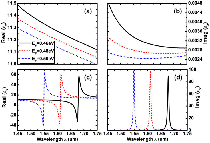
As an example, in Fig. 2(a)–(d) we plot the effective permittivity εx and εz as a function of the operation wavelength at the different Fermi energies at the near-infrared (NIR) frequency. Here, we assume that the Fermi-energy of graphene EF = 0.46, 0.48, and 0.50 eV, respectively. The other parameters are T = 300 K, τ = 0.5 ps, td = 8 nm, εd = 11.7; tg = M*0.35 nm, where M is the layer number of the graphene sheets, and M = 1 is for the single-layer graphene. It is seen from Fig. 2(a) and (b) that the real part of εz is positive, and both the real part and the imaginary part of εz vary with wavelength slowly. As the Fermi energy is increased, both the real part and imaginary part of εz decrease slightly. However, εx exhibits resonant behavior in NIR frequency. Re(εx) < 0 and Im(εx) become very large near the resonant wavelength λres. For EF = 0.50 eV, λres = 1.534 μm, at this frequency, Re(εx) < 0 and Re(εz) > 0. Hence Eq. (5) denotes a dispersion curve of hyperboloid. Furthermore, we find that the resonant wavelength of the hyperbolic dispersion curve can be electrically controlled by an applied gate voltage on the graphene sheets. It is clear that the resonant behavior of εx can be tuned by varying the Fermi energy. Increasing Fermi energy, the resonant wavelength λres shifts to the smaller wavelength; while decreasing Fermi energy results in the red shift of the resonant wavelength λres.
Figure 2.
(a) and (b) are the real and imaginary parts of εz, (c) and (d) are the real and imaginary parts of εx. The parameters are T = 300 K, τ = 0.5 ps, tg = M*0.35 nm, M = 1, td = 8 nm, εd = 11.7.
Critical coupling phenomena with graphene-based HMMs
The resonant behavior of εx can be used to design a CCR. We replace the polymer absorbing layer or the metal-dielectric composite film in the conventional CCRs by the graphene-based HMM, as shown in Fig. 1(a). The DBR (AB)NA is constituted by two dielectrics A and B with permittivity εA and εB and thickness tA and tB respectively. In the numerical calculations, we choose the following parameters: N = 10, εA = 5.7121 and εB = 2.6244. The thickness of dielectrics A and B are chosen to correspond to λ/4 plate: tA = λc/(4nA) and tA = λc/(4nB), where the central wavelength is chosen as λc = 1550 nm,  , and
, and  . To easily design and adjust the spatial distance ts, we assume that the space between the graphene-based HMM and DBR is filled by air.
Next, we show that CC can be realized in our structure. In Fig. 3 we give the absorption of CCR as a function of wavelength at the different Fermi energy EF. The thickness of spacer layer ts = 600 nm and the thickness of HMM tHMM = 10*(tg + td) = 83.5 nm are chosen to achieve nearly 100% absorption at the central wavelength λc = 1.534 um and EF = 0.5 eV, and the other parameters have the same values as those in Fig. 2. Compared to the absorption A ≈ 40% of the HMMs on the glass substrate, the absorption from the CCR is enhanced about 2.5 times. Hence, our structure becomes very efficient to maximize light absorption. Another advantage of our structure is the tunable CC frequency by changing the Fermi energy levels, as shown in Fig. 3, which are in consistent with the dependence of the effective permittivity εx on the Fermi energy as shown in Fig. 2(c). When we decrease the Fermi energy EF, the absorption peak moves to the longer wavelength side; when we increase the Fermi energy EF, the absorption peak moves to the longer wavelength side. For EF = 0.46 eV, the central wavelength is 1.661 μm; however for EF = 0.48 eV, the central wavelength λc is 1.594 μm. This property suggests that the frequency of absorption peak can be engineered by the Fermi energy of the graphene sheets. Although the absorption remains still high (>90%), either the decrease or increase in the Fermi energy level leads to the departure from the CC phenomenon.
Figure 3. The absorption of critically coupled resonance as a function of wavelength at different Fermi energy EF, where ts = 600 nm, tHMM = 83.5 nm, and the other parameters have the same values as those in Fig. 2(c).
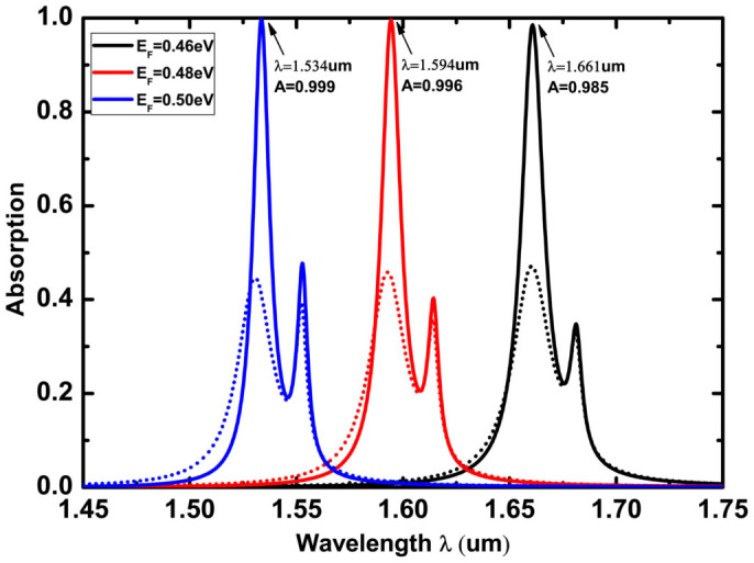
The dotted lines are the corresponding absorption of the HMMs on the glass substrate.
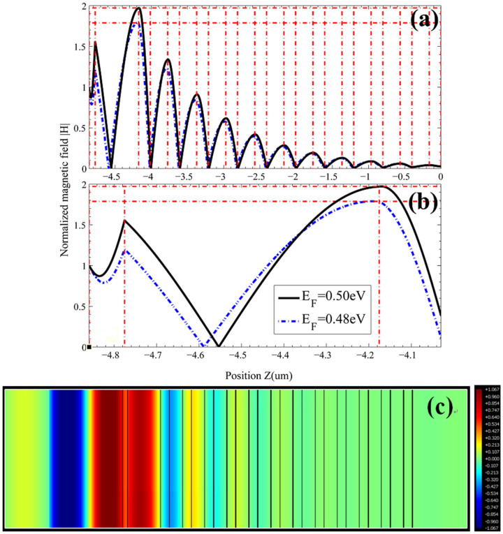
To understand the almost 100% absorption of the incident energy by the CCR at the CC frequency, we have plotted the magnetic field distributions inside the layered structure at the CC wavelength λ = 1.534 um for EF = 0.50 eV based on the transfer matrix method (TMM), as shown in the solid-line in Fig. 4(a) and (b). To confirm the correctness of TMM, in Fig. 4(c) we also provide the simulated magnetic field distributions by using the Finite-difference time-domain (FDTD)(The time evolution of magnetic field has been given in the Supplement materials). The magnetic field amplitude has been normalized to the incident magnetic field amplitude. One can see that the magnetic field is evanescent light wave in DBR due to the total reflection, however the magnetic field is strongly enhanced and localized in the graphene-based HMM and spacer. The large intensity enhancement and large imaginary parts of εx in the absorption layer of graphene-based HMM, explains the CC phenomenon (near-perfect light absorption) at the CC wavelength λc = 1.534 um for EF = 0.50 eV. Additionally, for comparison, in Fig. 4(a) and (b) we have plotted the normalized magnetic field distributions for λ = 1.594 um at EF = 0.48 eV. It is clear that those magnetic fields are weaker than the field at EF = 0.50 eV, explaining why there is a departure from the CC phenomenon at EF = 0.48 eV. Hence, in order to achieve the CC at the different Fermi energy levels, we must optimize the physical parameters, such as, the fill factors of the dielectric and graphene sheet in the HMMs, the thickness of spacer layer ts, and the thickness of HMMs tHMM. However, to realize the tunability of the CC frequency by changing the Fermi energy in a fixed configuration, we intend to finely adjust the distance between the graphene-based HMM and DBR on glass substrate, i.e. the thickness of spacer layer ts. The optimization is given as following.
Figure 4. The magnetic field distributions in the critically coupled resonance at different Fermi energy EF, (b) is the enlarged view of (a) in the graphene-based HMMs and spacer, (c) is the magnetic field distributions gotten by FDTD method for EF = 0.50 eV and λ = 1.534 um.
EF = 0.50 eV and λ = 1.534 um, and EF = 0.48 eV and λ = 1.594 um are for the solid-line and dashed-dotted line, respectively. Other parameters are as in Fig. 2, the red dashed-dotted lines in (a) and (b) and solid-line in (c) show the interface of different materials.
Recover the CC at the different Fermi energy levels
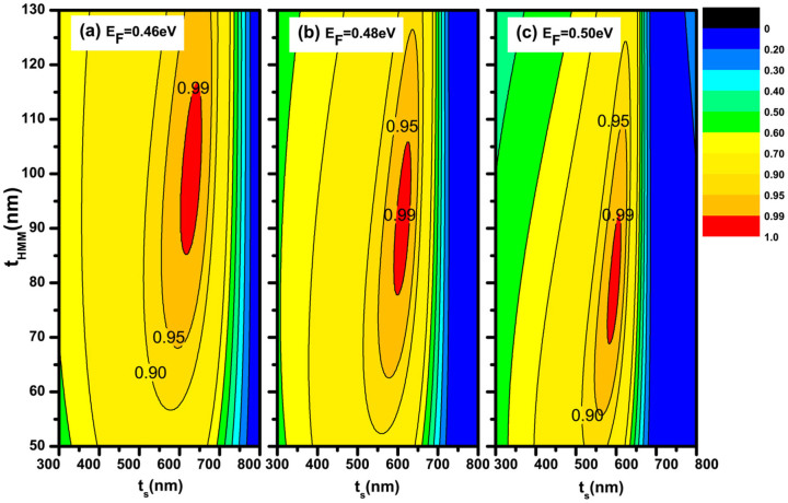
To recover the CC at the different Fermi energy, we have plotted the contours of the absorption of the CCR as a function of the thickness of the spacer layer ts and the thickness of the HMMs at the different Fermi energy EF, as shown in Fig. 5. The red region gives the absorption larger than 99%, here we consider it as the CC region. It is obvious that both ts and tHMM should be decreased with the increase of Fermi energy. To easily adjust this property in the experiments, we intend to find the common area of the thickness tHMM for the CC at the different Fermi energies. It is found that this region is located near tHMM = 88 nm. The optimized results have been demonstrated in Fig. 6. Here we keep the thickness of HMM tHMM = 88 nm fixed, and adjust the distance ts. According to the optimized results in Fig. 5, we choose ts = 590 nm for EF = 0.50 eV, ts = 610 nm for EF = 0.48 eV, and ts = 650 nm for EF = 0.46 eV. It is clear from Fig. 2 that, for λ = 1.661 um at EF = 0.46 eV departure from CC, one can recover CC just by adjusting the distance ts = 650 nm. For λ = 1.594 um at EF = 0.48 eV, CC resonance can be recovered by increasing the distance ts to 610 nm. Therefore, our CCR has the potential to achieve tunable CC frequency in a fixed configuration.
Figure 5. The contours of the absorption of critically coupled resonance as a function of thickness of spacer layer ts and thickness of HMMs at the different Fermi energy EF.
Where EF = 0.52 eV and λ = 1.478 um in (a), EF = 0.50 eV and λ = 1.534 um in (b), and EF = 0.48 eV and λ = 1.594 um in (c). Other parameters are as in Fig. 2.
Figure 6. The absorption of critically coupled resonance as a function of work wavelength at different Fermi energy EF.
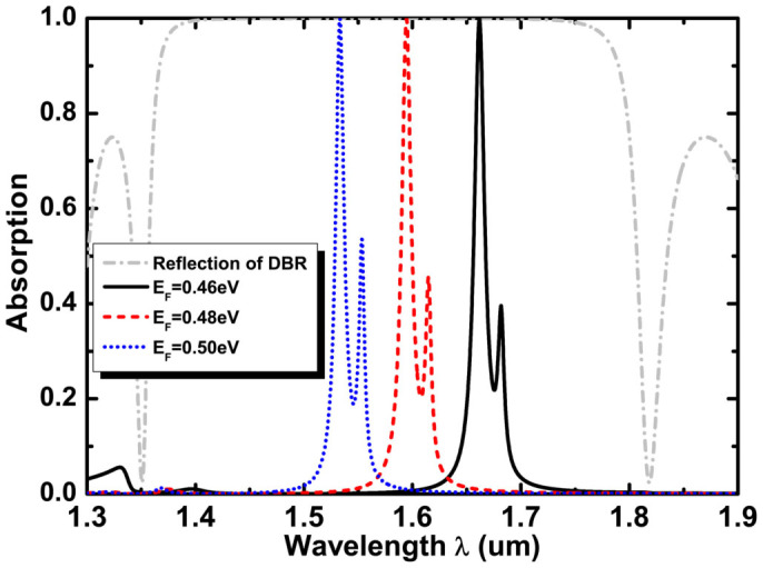
Where ts = 590 nm for EF = 0.50 eV, ts = 610 nm for EF = 0.48 eV, and ts = 650 nm for EF = 0.46 eV, tHMM is kept as constant 88 nm. Other parameters are as in Fig. 2. The gray dashed-dotted line gives the reflection of DBR on the glass substrate.
Critical coupling phenomena at two frequencies
From Fig. 3, it is found that there are two absorption peaks in the layered structure. In Fig. 6 we have recovered the CC at the different Fermi energy for one peak. But how can we realize the CC phenomena at two distinct frequencies? By optimizing the parameters of the structure, including ts and tHMM, we have plotted the absorption coefficient as a function of wavelength, as shown in Fig. 7. We have used different sets of values for different Fermi energies. For EF = 0.50 eV we used tHMM = 16*(tg + td); for EF = 0.48 eV we used tHMM = 17*(tg + td); for EF = 0.46 eV we used tHMM = 19*(tg + td), where M = 1 and ts = 500 nm. It is clear that for optimal values of the thickness of graphene-based HMMs we can obtain CC at two distinct frequencies.
Figure 7. The critical coupling phenomena at two distinct wavelengths at different Fermi energy EF.
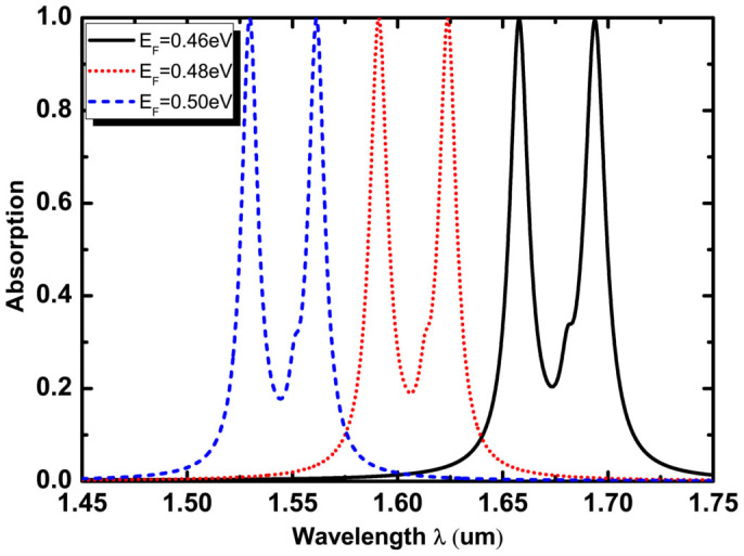
For EF = 0.50 eV we used tHMM = 16*(tg + td); for EF = 0.48 eV we used tHMM = 17*(tg + td); for EF = 0.46 eV we used tHMM = 19*(tg + td), where M = 1 and ts is kept as constant 500 nm. Other parameters are as in Fig. 3.
Discussion
In addition to Fermi energy, the resonant behavior of εx also depends on the fill factions of dielectric and graphene sheet. Decrease in thickness of dielectric td or increase in layer number of graphene sheets M leads to the decrease of fill factor of dielectric fd and the increase of fill factor of dielectric fg, so that the graphene sheets are becoming more and more important in the HMMs. These properties are significant for controlling CC due to the strong dependence of the CC behavior on the resonant behavior of εx, while the results are shown in Fig. 8. The solid lines are the CC phenomenon at the central wavelength λ = 1.534 um and EF = 0.5 eV, the parameters are the same as those in Fig. 3. In Fig. 8(a), it is found that the central frequency of the absorption peak shifts towards longer wavelength side with increasing the layer number of the graphene sheets M. The absorption peak departs from the CC phenomenon, which may be optimized by varying tHMM or ts as shown in Fig. S1 of the Supplementary materials. In Fig. 8(b), we find that the central frequency of the absorption peak shifts to longer wavelength side with decreasing td and shifts to shorter wavelength side with increasing td, the optimization result is given in Fig. S2 of the Supplementary materials. In Fig. 8(c), we show the absorption as a function of wavelength at different relaxing time τ. It is clear that the central frequency of the absorption peak keeps fixed and the absorption decreases with the decreased or increased relaxing time, the optimization result is given in Fig. S3 of the Supplementary materials. According to above analyses, it is demonstrated that the dependence of absorption on the resonant behavior of εx provides more degree of freedom to control the CC phenomenon at the NIR frequencies by using graphene-based HMMs.
Figure 8. The absorption as a function of work wavelength at the different layer number of graphene sheets (a), thickness of dielectric in graphene-based HMM (b) and relaxing time (c).
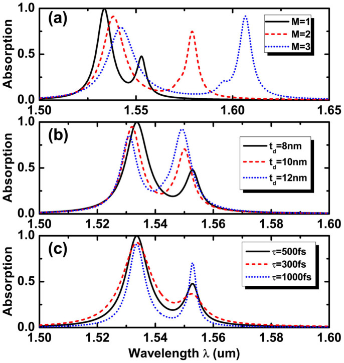
Where td = 8 nm and τ = 500 fs in (a), M = 1 and τ = 500 fs in (b), and td = 8 nm and M = 1 in (c), other parameters are as in Fig. 3.
In conclusion, we have presented a graphene-based HMM as the absorbing thin film to realize the CC phenomenon in the NIR frequency regime and discussed the controllable properties of this phenomenon in the CCR. It is found that the CC phenomenon depends on the resonant behavior of the effective permittivity of HMMs, and the CC frequency can be effectively tuned by changing the Fermi energy level applied on the graphene sheets. However, near-perfect absorption departs from the CCR if the Fermi energy is significantly changed. Hence, to recover the CC phenomenon optimization on the thickness of dielectric, the layer number of graphene sheets in HMMs, and the relaxation time of graphene sheet need to satisfy certain requirements. The optimization results are also presented. We believe that the controllable CC phenomenon and near-perfect absorption at the NIR frequencies (telecommunication band) could find potential applications in optical communications, optical detectors and photovoltaic.
Methods
The numerical calculations for the effective permittivities of the graphene-based hyperbolic metamaterials, the theoretical absorption spectrum, and the optimization results of critical coupling phenomena in the critically coupled resonant containing graphene-based hyperbolic metamaterials were generated using Matlab code based on the transfer matrix method. Let a plane wave be injected from vacuum into the critically coupled resonant at normal incidence with +z direction. Generally, the electric and magnetic fields at any two positions z and z + Δz in the same layer can be related via a transfer matrix,
 |
where i denote the different media,  is the components of the wave vector along the z axis in the isotropic medium. For the TM polarization,
  and qz = kz/k0εx in the hyperbolic metamaterial, qiz = kiz/k0εi in the isotropic medium. The reflection and transmission coefficients can be calculated as
 |
 |
Hence, the absorption can be obtained as,
 |
where Xij(i,j = 1,2) are the matrix elements of Xi,j(ω) = ΠMi(Δz,ω), which represent the total transfer matrix connecting the fields at the incident end and the exit end;  , ε1 and εL are the permittivity of the media before the incident end and the space after the exit end, respectively.
Author Contributions
Y.J.X. and X.Y.D. performed derivation of formulas and wrote the manuscript. J.G. helped in numerical calculations. H.Z., S.C.W. and D.Y.T. conceived the idea and co-wrote the manuscript. All authors discussed the results and commented on the manuscript.
Supplementary Material
Supplementary Information
The time evolution of magnetic field
Acknowledgments
This work is partially supported by the Minister of Education (MOE) Singapore under the grant no. 35/12, Natural Science Foundation of Hunan Province of China (Grant No. 12JJ7005), the National Natural Science Foundation of China (Grant No. 11004053), and the Ph.D. Programs Foundation of Ministry of Education of China (Grant No. 20120161120013).
References
- Novoselov K. S. et al. Electric field effect in atomically thin carbon films. Science 306, 666–669 (2004). [DOI] [PubMed] [Google Scholar]
- Neto A. H. C., Guinea F., Peres N. M. R., Novoselov K. & Geim A. K. The electronic properties of graphene. Rev. Mod. Phys. 81, 109–162 (2009). [Google Scholar]
- Grigorenko A. N., Polini M. & Novoselov K. S. Graphene plasmonics. Nat. Photonics 6, 749–758 (2012). [Google Scholar]
- Liu M. et al. A graphene-based broadband optical modulator. Nature 474, 64–67 (2011). [DOI] [PubMed] [Google Scholar]
- Vakil A. & Engheta N. Transformation optics using graphene. Science 332, 1291–1294 (2011). [DOI] [PubMed] [Google Scholar]
- Koppens F. H. L., Chang D. E. & García de Abajo F. J. Graphene plasmonics: A platform for strong light-matter interactions. Nano Lett. 11, 3370–3377 (2011). [DOI] [PubMed] [Google Scholar]
- Bao Q. L. & Loh K. P. Graphene Photonics, Plasmonics, and Broadband Optoelectronic Devices. ACS Nano 6, 3677–3694 (2012). [DOI] [PubMed] [Google Scholar]
- Zhang H., Virally S., Bao Q. L., Loh K. P., Massar S., Godbout N. & Kockaert P. Z-scan measurement of the nonlinear refractive index of graphene. Opt. Lett. 37, 1856–1858 (2012). [DOI] [PubMed] [Google Scholar]
- Thongrattanasiri S., Koppens F. H. L. & García de Abajo F. J. Complete optical absorption in periodically patterned graphene. Phys. Rev. Lett. 108, 047401 (2012). [DOI] [PubMed] [Google Scholar]
- Ferreira A., Peres N. M. R., Ribeiro R. M. & Stauber T. Graphene-based photodetector with two cavities. Phys. Rev. B 85, 115438 (2012). [Google Scholar]
- Ferreira A. & Peres N. M. R. Complete light absorption in graphene-metamaterial corrugated structures. Phys. Rev. B 86, 205401 (2012). [Google Scholar]
- Nikitin A. Y., Guinea F. & Martin-Moreno L. Resonant plasmonic effects in periodic graphene antidot arrays. Appl. Phys. Lett. 101, 151119 (2012). [Google Scholar]
- Nefedov I. S., Valaginnopoulos C. A. & Melnikov L. A. Perfect absorption in graphene multilayers. J. Opt. 15, 114003 (2013). [Google Scholar]
- Tischler J. R., Bradley M. S. & Bulović V. Critically coupled resonantors in vertical geometry using a planar mirror and a 5 nm thick absorbing film. Opt. Lett. 32, 2045–2047 (2006). [DOI] [PubMed] [Google Scholar]
- Tischler J. R. et al. Solid state cavity QED: strong coupling in organic thin films. Org. Electron. 8, 94–113 (2007). [Google Scholar]
- Gupta S. D. Strong-interaction-mediated critical coupling at two distinct frequencies. Opt. Lett. 32, 1483–1485 (2007). [DOI] [PubMed] [Google Scholar]
- Deb S., Gupta S. D., Banerji J. & Gupta S. D. Critical coupling at oblique incidence. J. Opt. A: Pure Appl. Opt. 9, 555–559 (2007). [Google Scholar]
- Deb S. & Gupta S. D. Critical coupling in a Fabry–Pérot cavity with metamaterial mirrors. Opt. Commun. 283, 4764–4769 (2010). [Google Scholar]
- Reddy K. N., Gopal A. V. & Gupta S. D. Nonlinearity induced critical coupling. Opt. Lett. 38, 2517–2520 (2013). [DOI] [PubMed] [Google Scholar]
- Iorsh I. V., Mukhin I. S., Shadrivov I. V., Belov P. A. & Kivshar Y. S. Hyperbolic metamaterials based on multilayer graphene structures. Phys. Rev. B 87, 075416 (2013). [Google Scholar]
- Othman M. A. K., Guclu C. & Capolino F. Graphene-based tunable hyperbolic metamaterials and enhanced near-field absorption. Opt. Express 21, 7614–7632 (2013). [DOI] [PubMed] [Google Scholar]
- Sreekanth K. V., De Luca A. & Strangi G. Negative refraction in graphene based metamaterials. Appl. Phys. Lett. 103, 023107 (2013). [Google Scholar]
- Zhang T., Chen L. & Li X. Graphene-based tunable broadband hyperlens for far-field subdiffraction imaging at mid-infrared frequencies. Opt. Express 21, 20888–20899 (2013). [DOI] [PubMed] [Google Scholar]
- Chen P. Y. & Alù A. Atomically thin surface cloak using graphene monolayers. ACS Nano 5, 5855–5863 (2011). [DOI] [PubMed] [Google Scholar]
- Hanson G. W. Dyadic Green's functions and guided surface waves for a surface conductivity model of graphene. J. Appl. Phys. 103, 064302 (2008). [Google Scholar]
- Gusynin V. P., Sharapov S. G. & Carbotte J. P. Magneto-optical conductivity in graphene. J. Phys.: Condens. Matter 19, 026222 (2007). [Google Scholar]
Associated Data
This section collects any data citations, data availability statements, or supplementary materials included in this article.
Supplementary Materials
Supplementary Information
The time evolution of magnetic field


