Abstract
Objective
We focus on improving the long-term stability and functionality of neural interfaces for chronic implantation by using bilayer encapsulation.
Approach
We evaluated the long-term reliability of Utah electrode array (UEA) based neural interfaces encapsulated by 52 nm of atomic layer deposited (ALD) Al2O3 and 6 μm of Parylene C bilayer, and compared these to devices with the baseline Parylene-only encapsulation. Three variants of arrays including wired, wireless, and active UEAs were used to evaluate this bilayer encapsulation scheme, and were immersed in phosphate buffered saline (PBS) at 57 °C for accelerated lifetime testing.
Main results
The median tip impedance of the bilayer encapsulated wired UEAs increased from 60 kΩ to 160 kΩ during the 960 days of equivalent soak testing at 37 °C, the opposite trend as typically observed for Parylene encapsulated devices. The loss of the iridium oxide tip metallization and etching of the silicon tip in PBS solution contributed to the increase of impedance. The lifetime of fully integrated wireless UEAs was also tested using accelerated lifetime measurement techniques. The bilayer coated devices had stable power-up frequencies at ~910 MHz and constant RF signal strength of -50 dBm during up to 1044 days (still under testing) of equivalent soaking time at 37 °C. This is a significant improvement over the lifetime of ~ 100 days achieved with Parylene-only encapsulation at 37 °C. The preliminary samples of bilayer coated active UEAs with a flip-chip bonded ASIC chip had a steady current draw of ~ 3 mA during 228 days of soak testing at 37 °C. An increase in current draw has been consistently correlated to device failures, so is a sensitive metric for their lifetime.
Significance
The trends of increasing electrode impedance of wired devices and performance stability of wireless and active devices support the significantly greater encapsulation performance of this bilayer encapsulation compared with Parylene-only encapsulation. The bilayer encapsulation should significantly improve the in vivo lifetime of neural interfaces for chronic implantation.
Keywords: Utah Electrode Array, Neural Interface, Brain Machine Interface, Long-term Reliability, Atomic Layer Deposited (ALD) Al2O3, Parylene, Bilayer encapsulation, Biomedical Implantable Devices
2 Introduction
Implantable neural interfaces have been widely developed and also used to diagnose and treat neural disorders in both research and clinical applications [1-6]. The Utah electrode array (UEA) is a well-developed and FDA-cleared example of this technology for stimulating/recording multiple neurons simultaneously with good selectivity [5, 7-9]. Traditionally, UEAs use gold wire bundles and percutaneous connectors to transfer recording/stimulation signals. However, percutaneous connectors and wire bundles are more likely to cause foreign body response [10] and promote infections [11] during chronic implantations. In addition, percutaneous connectors have been found to be one of the least reliable elements of neural interfaces [12]. Therefore, tremendous efforts have been devoted to develop neural interfaces with wireless transmission of power and data [13-18], to eliminate wire bundles. Fully integrated wireless neural interfaces based on UEAs have been developed with recording and stimulating capabilities from 100 channels [16, 18].
Both wired and wireless neural interfaces are designed to function in vivo for years for chronic implantation and used to evaluate the Al2O3 and Parylene bilayer encapsulation. Factors that compromise the performance of chronic neural interfaces can include physiological reasons (e.g. foreign body responses) and device failure modes (encapsulation failure). Encapsulation failure can lead to short circuits, corrosion of components and interconnects, which are often catastrophic especially for wireless neural interfaces with integrated active electronics. The significant bias voltages associated with integrated electronics further challenge thin film encapsulation by activating degradation modes and accelerating ion transport. Protecting implanted devices has typically utilized hermetic enclosures and thin film encapsulation approaches. Lids and metal cans are used to seal implantable devices, e.g. deep brain stimulators and pacemakers [19], in order to protect them from the physiological environment. Device miniaturization, electromagnetic power, and telemetry schemes are challenges for traditional hermetic encapsulation. Thin film encapsulation methods have been widely developed and used for small implants, and are compatible with electromagnetic wireless techniques. Different materials have been investigated for coating of neural interfaces, including polyimide[20], Parylene [21, 22], silicone[23], amorphous silicon carbide [24, 25], silicon nitride [25], and diamond-like carbon (DLC) [26]. Finding one material that meets all the requirements for coating neural interfaces is extremely difficult. For example, silicon nitride slowly dissolves in PBS[25]; amorphous silicon carbide and DLC need relatively high deposition temperatures that are not compatible with devices; polyimide is very difficult to deposit uniformly.
Parylene C has been widely used as coating material for biomedical implantable devices [22, 27-30] due to its attractive properties including chemical inertness, low dielectric constant (εr=3.15) [31], high resistivity (~1015 Ω·cm) and relatively low water vapor transmission rate (WVTR) of 0.2 g·mm/m2·day [32]. It can be deposited by chemical vapor deposition (CVD) at room temperature to generate a conformal and pin-hole free film that does not require use of solvents to form. Parylene is also a good ion barrier [33], which is critical for neural interfaces exposed to physiological fluids.
Parylene cracking has been observed during in-vivo experiments [34]. Cracks occurred on the Parylene coating films (3 μm thick) of the electrode arrays that were implanted in cats for 537 days. Failure of Parylene C encapsulation has also been reported [35] due to moisture diffusion and interface contamination. Surface contaminants or voids between substrate and encapsulation are required for the nucleation of moisture into liquid water. To overcome the condensation of moisture around interface contaminants, a highly effective moisture barrier can be introduced between the neural interface and Parylene film. Atomic layer deposited (ALD) alumina is an excellent moisture barrier with WVTR at the order of ~ 10-10 g·mm/m2·day [36-39], and is extremely conformal, which allows it to passivate surfaces that are otherwise difficult to cover. But alumina alone is not a suitable encapsulation since it dissolves in water [40], which allows body fluids to contact with the device underneath the encapsulation easily. The alumina-Parylene C bilayer encapsulation has demonstrated excellent insulation performance on planar interdigitated electrode (IDE) test structures for years of equivalent lifetime in accelerated soak testing[41-43]. This approach utilizes the highly effective moisture barrier property of ALD Al2O3, and Parylene C as an ion barrier and for preventing contact between alumina and liquid water. Test structures are good for optimizing the properties and conditions to get good films, but we have previously observed significant differences in lifetimes of IDEs compared to real systems. The complex geometries (gold coils and SMD capacitors), different materials and surfaces, and additional processing steps (oxygen plasma etching, BOE etching, wire bonding) involved in neural interfaces are not fully represented in IDE test structures and therefore might severely affect the actual lifetime of the bilayer encapsulated neural interfaces.
In this paper, we evaluated the long-term reliability of ALD Al3O3 and Parylene C bilayer coated UEA based neural interfaces. The bilayer encapsulated neural interfaces were submerged in PBS at 57 °C for accelerated lifetime testing. The bilayer encapsulation performance was evaluated from a few different aspects: electrode tip impedance by wired UEAs, wireless powering up frequencies and signal strengths by wireless UEAs, and current draw levels by active arrays. Similar to wireless arrays, active arrays have flip-chip bonded chips for signal processing, and wires for powering and communication. Detailed description is shown in next section.
3 Experimental Details
3.1 Integrated Neural Interfaces
Three different configurations of UEA-based neural interfaces were used to evaluate the alumina and Parylene C bilayer encapsulation performance. Traditional wired UEAs, fully integrated wireless arrays, and active arrays were used to evaluate the bilayer encapsulation from three different aspects: long-term impedance stability, long-term wireless signal strength and frequency stability, and the level of current draw, respectively. Fabrication and testing procedures used to evaluate the encapsulation are presented in this section.
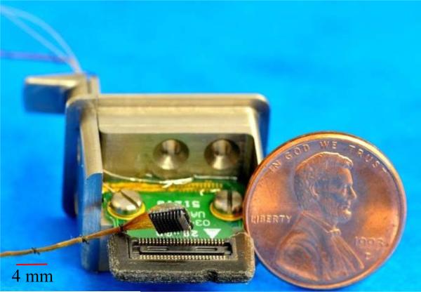
The UEA was first designed and fabricated by Normann for intracortical stimulation [44]. A dicing saw was used to cut silicon wafer and create columns with dimension of 150 μm square, 1.5 mm in length, and a pitch of 400 μm. The columns were first thinned and then tapered by wet etching. The fabrication details of UEAs are described elsewhere [44, 45]. Wired UEAs were used to evaluate the electrode impedance stability over time. UEAs were wire bonded (West Bond, Inc.) to a 96-channel TDT™ connector (Tucker-Davis Technologies) using 1 mil insulated gold wire with a wirebundle length of 10 cm for long-term tip impedance measurements (Fig 1). Silicone (MED 4211, NuSil Technology) was applied to the backside of the array and the wire bundle to secure the bond connections, increase the strength of the wire buddle, and further protect the array from handling forces and fluid ingress. The fully integrated wired UEAs were then coated with Al2O3 and Parylene C bilayer, as described later.
Fig 1.
A fully assembled wired Utah electrode array with connector for impedance measurement. The Ti pedestal is part of the connector system.
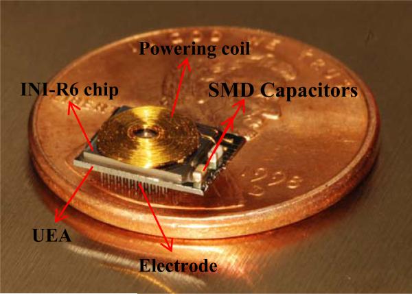
The performance of the bilayer encapsulation was further tested by using wireless integrated neural interfaces, and soaking these in PBS under accelerated conditions. The ability to power the devices inductively, and the associated telemetry frequencies on power-up, and the RF signal strengths were used as sensitive metrics for the encapsulation performance and fluid ingress. This device uses a 100-channel wireless neural recording IC, designated as INIR-6 (integrated neural interface recording version-6), that was fabricated with 0.6 μm BiCMOS process (X-fab semiconductors). The details of the chip design, fabrication, characterization, and system integration were reported elsewhere [16, 18, 46]. An INIR-6 chip with capabilities of signal processing and data telemetry was flip-chip bonded to the backside of a 10×10 UEA using Au/Sn reflow soldering. Two SMD capacitors were soldered to the backside of the UEA and connected to the chip via backside metal traces. One SMD was part of the resonating circuit for inductive powering and the other was a smoothing capacitor for the DC power supply. A flat spiral coil of 5.5 mm in diameter was manufactured by winding an insulated 2-mil Au (1% Pd) wire [47]. The gold coil was wire-bonded to form the resonating circuit around 2.765 MHz with the SMD capacitor for inductively powering up the device. The fully integrated wireless INI is shown in Fig 2.
Fig 2.
Utah electrode array based fully integrated wireless neural interfaces, with flip-chip bond INI-R6 and gold coil for inductive powering.
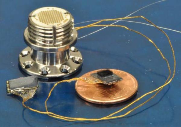
Active array, another version of neural interfaces, was built to monitor the current draw of neural interfaces over time under soak testing, as show in Fig 3. The details of active arrays were reported elsewhere [48]. It was similar to the wireless neural interfaces with a flip-chip bonded ASIC for amplification, analog multiplexing, and signal buffering. Instead of inductive powering and wireless communication, active arrays used 22 wire-bonded gold wires for data transferring and powering. In this way, the current draw between power rails can be directly monitored.
Fig 3.
An active array assembly that includes 2 arrays and 2 reference wires connected to a single Neuroport™ connector (100 bond pads). Compared with a 100-channel wired array requiring 100 wires, only 22 wires are needed for each active array, which makes it possible to improve the recording/stimulation capabilities by connecting 2 active arrays (200 channels) to one connector.
3.2 Alumina and Parylene C Deposition
52 nm of Al2O3 was deposited by plasma-assisted (PA) ALD on integrated neural interfaces at a substrate temperature of 120 °C, which is within the thermal budget for the materials used for the three array variants. Details of the deposition process have been previously reported [41, 42, 49, 50]. A-174 (Momentive Performance Materials), an organosilane, was used as an adhesion promoter between the alumina and Parylene C layer. A 6-μm thick Parylene-C layer was deposited by CVD using the Gorham process [31] on top of Al2O3 as the external coating layer. For wired neural interfaces, the connectors were covered with aluminum foil to avoid coating of the contact pads on the connectors.
3.3 Tip Deinsulation
The encapsulation must be removed from the active tip electrodes sites for neural recording and stimulation. Traditionally, oxygen plasma reactive ion etching (RIE) was used to remove the Parylene C on the tips by poking the tips through aluminum foil. However, this method does not etch alumina. Additionally, it is extremely challenging to control the tip exposure with an uneven backside during the poking process, especially for Utah Slant Electrode Arrays (USEAs).
A hybrid method using a combination of laser ablation and O2 RIE was utilized to etch Parylene C layer and buffered oxide etch (BOE) was used to remove the thin alumina film [51]. First, an Optec Micromaster excimer laser micromachining system was used for ablation of Parylene C. 200 laser pulses with fluence of 1400 mJ/cm2 were applied with 5 ns pulses at 100 Hz to remove the outer Parylene C film from the electrode tips. The alumina layer underneath Parylene acted as a shield layer, protecting the tip metallization (sputtered iridium oxide film (SIROF)) from being damaged by heating/ablation from laser radiation. The laser deinsulation process resulted in carbon residue and redeposition on the surface, which was removed by utilizing 2 minutes of O2 RIE. The alumina layer was then etched by dipping the array into BOE for 8 minutes. Parylene C acted as a mask layer for BOE etching, with the alumina etch occurring only in the areas where Parylene was removed by laser, generating a self-aligned process. The tip exposure was about 35 μm. The lifetime metrics of these devices were then tested by placing them in PBS under accelerated testing conditions.
3.4 Testing setup
Wired arrays were used for long-term impedance measurements, and were soaked in 1× PBS (10 mM phosphate buffer, 2.7 mM KCl and 140 mM NaCl) at 57 °C for accelerated lifetime testing. The estimated aging factor (Q) was 4, based on a broadly recognized trend in accelerated aging of a doubling reaction kinetics for each 10 °C increase in reaction temperature[52, 53]. The PBS solution was changed every other week to minimize changes in the composition (ion concentrations), and their effects on impedance. Tip impedance was measured by connecting the TDT™ connector with a customized automated impedance tester (AIT), using two platinum wires as reference and counter electrodes, respectively [54]. The tip impedance measurement was obtained by electrically connecting all non-tested electrodes to ground potential, which was different from conventional impedance, where all non-tested electrodes were electrically floating. The impedance tester automatically switched between channels and measured impedance for all channels at 1 kHz with a 10 mV sine wave. The measurable impedance range for AIT was 300 Ω - 10 MΩ.
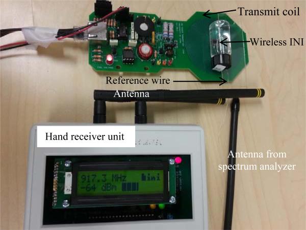
For wireless neural interface testing, the arrays were fully submerged in 6-ml glass vials filled 1× PBS at 57 ± 0.5 °C in water baths. The experimental setup was shown in Fig 4. The wireless neural interfaces were powered by a customized inductive power board at 2.765 MHz that was previously reported [16]. The receiving antennas for both the spectrum analyzer and hand receiver were brought close to the reference wires of the INI device to get reliable RF reception. The INI device was about 8 mm away from the power coil, and the device was powered up only during testing. The presence of the 900-MHz ISM-band telemetry signal, the frequency of that signal on startup, and RF signal strength from INIR-6 chip were monitored using the customized receiver board interfaced through Matlab and with a spectrum analyzer [16].
Fig 4.
Experimental setup for wireless integrated neural interface testing. The antennas were brought close to the reference wire from the INI device. The device is ~ 8 mm away from the power board.
The current draw is an important metric for evaluating the performance of encapsulation for devices with active electronics, and has been found to be a sensitive indicator of the encapsulation performance for these devices. The wireless INIs are not capable of measuring the current; therefore, another version of UEAs with flip-chip bonded ASIC chips (without wireless capability) on the backside was used to monitor the current draw of the device over time under soak testing [48]. The active arrays were soaked in glass vials filled with 1× PBS solution at 57 °C and powered up only during the measurement of current draw. The current draw of the ASIC chip was measured with power supply of +1.5 V and -1.5 V to Vdd and Vss, respectively.
4 Results and Discussion
4.1 Wired Utah Electrode Arrays
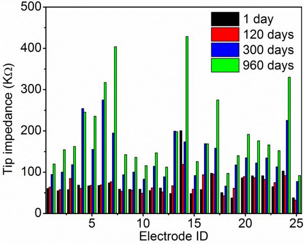
Impedance for wired array was measured at 1 kHz using 10-mV sine wave. These wired arrays have gone through the bilayer coating process, and associated hybrid deinsulation process. Very high impedances (in MΩ range, 6 out of 50 electrodes) were excluded from the plot since this most often results from chipped-tips or broken electrodes. As shown in Fig 5, tip impedances were found to range from 30 to 100 kΩ for most electrodes, with a median impedance of 60 kΩ. Those impedance values are good for neural interface applications, and consistent with previously reported data [22]. The non-uniformity of impedance results mostly from variations (dicing and etching non-uniformity, tip metal thickness variation, etc.) in resultant manufactured samples. The impedance of alumina and Parylene coated UEAs stayed almost the same during equivalent soaking time of first 120 days at 37 °C (non-accelerated conditions), indicating good insulation of individual electrodes. Impedance for Parylene-only control samples consistently dropped within a few weeks to 3 months [7, 55]. Table 1 compares the median of tip impedance for Parylene-only and bilayer coated UEAs. For the Parylene-only condition, the median tip impedance dropped from 81.9 kΩ to 40.5 kΩ within 3 days of soak testing. The significant impedance drop is most likely due to water ingress and degradation of the Parylene coating. For alumina and Parylene bilayer coating, the median of tip impedance increased slightly from 61.1 kΩ to 73.8 kΩ within 3 days. As described below, etching of exposed silicon at the electrode tips, and undercutting of the tip metallization are the mechanisms for the increased impedance. In terms of encapsulation performance, the relative change of the impedance is more important than its absolute value. The absolute value is pre-determined by factors like the manufacturing process and tip exposure. The change of the impedance during soak testing is affected by the encapsulation performance and lifetime.
Fig 5.
Electrode impedance of alumina and Parylene bilayer coated wired arrays over time. Only 25 out of 50 tip impedances were shown due to the limited space. Median impedance was 60 kΩ. The impedance stayed almost the same for each electrode over the first 120 days at 37 °C, and increased ~ 2.5 times (calculated from median impedance) after 960 days of soak testing in PBS.
Table 1.
The median impedance for Parylene coated UEA and alumina and Parylene bilayer coated UEA for 3 days of soak testing in PBS. The median impedance dropped ~ 50% after 3 days in PBS for Parylene coated UEA while it increased slightly for alumina and Parylene coated UEA.
| Soak time | Median impedance for Parylene coated UEA (kΩ) | Median impedance for bilayer coated UEA (kΩ) |
|---|---|---|
| 1 day | 81.9 | 61.1 |
| 3 days | 40.5 | 73.8 |
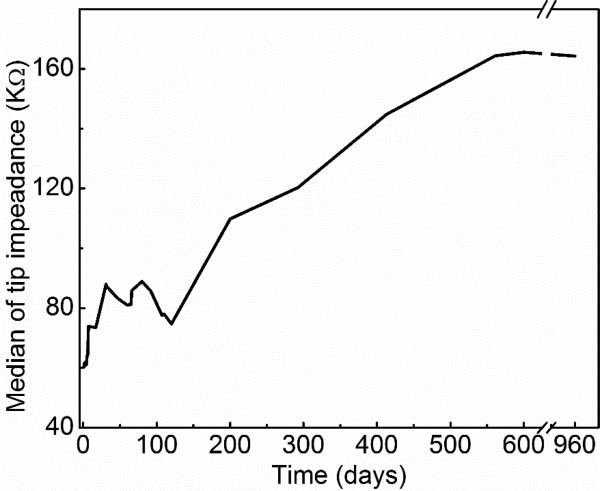
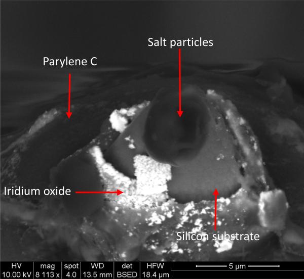
The tip impedance started increasing after 120 days of soak testing at 37 °C, as shown in Fig 5 and 6. The median tip impedance was about 160 kΩ after 960 days of soak testing, which is about 2.5 times of the median impedance at the first day (60 kΩ). This is the opposite trend of what we have observed from Parylene C coated tip impedance. Typically, impedance of Parylene C coated tips would decrease as a function of soaking time in a relatively short term (from days to a few months) due to water ingress and degradation of the coating [7, 55]. The increase in impedance of alumina and Parylene coated tips suggests a combination of dramatically less decreases in impedance from solution ingress, and loss of tip metal (SIROF) due to silicon etching in PBS generating an increase in measured impedance. The good encapsulation performance of the bilayer keeps the tip impedance relatively constant. The etching of silicon and loss of iridium oxide tip metal were confirmed by SEM images shown in Fig 7. This representative micrograph clearly shows that a large portion of the iridium oxide is gone on the electrode tip and there is a gap between the iridium oxide and silicon shank.
Fig 6.
Median tip impedance over time at 37 °C in PBS. The median of impedance stayed relatively stable during the first 120 days of soak testing and then started to increase over soaking time.
Fig 7.
Backscattered SEM micrograph of electrode tip after 960 days of soak testing at 37 °C. Silicon underneath iridium oxide (tip metal) was etched by PBS solution and iridium oxide was peeled off from the tip.
It is well known that PBS etches silicon [56]. The removal of underneath silicon substrate led to free-standing iridium oxide. Loss of the fragile iridium oxide can happen easily due to lack of support. We started to see MΩ range impedance for ~ 5 electrodes and expect to see further increases in the impedance as more silicon is etched and more iridium oxide is lost. We have measured the impedance of the similar silicon electrode tips without the tip iridium oxide metallization and the impedance was about 3-6 MΩ. This is consistent with what we have observed for those electrodes that have lost iridium oxide. Regarding Parylene coated electrodes, the degradation of encapsulation leads to decrease in impedance and loss of iridium oxide due to silicon etching would increase the impedance. The overall impedance drop of Parylene coated UEA indicates that the degradation of encapsulation dominates and offsets the impedance increase from tip metal loss. This also strongly indicates that alumina and Parylene bilayer coating has better insulation performance than the Parylene-only coating.
Wireless integrated neural interface (INI) devices were soaked at 57 °C in PBS for 261 days (equivalent soak time of 1044 days at 37 °C) and are still under soak testing to investigate the long-term reliability of alumina and Parylene C bilayer encapsulation. The presence of the signal, the startup frequencies, and the RF signal strengths of the INI device at different soak time were compared in Table 2. If the encapsulation fails and water ingress occurs then the device shorts out. Limited water ingress can also shift the telemetry frequency due to capacitive loading of the coil on the front of the ASIC (distinct from the hand-wound gold coil on the back of the device). When the device was in air, the telemetry frequency at powered-up was at 910.5 MHz with RF signal strength of -80 dBm measured using a spectrum analyzer. The RF signal strength increased to -75 dBm after the immersion of the device in PBS (Table 2). The custom-built hand receiver confirmed the increase of RF strength from -61 dBm to -47 dBm after submerging the device into PBS. The initial increase in RF signal strength is most likely due to the change of media from air to PBS solution, and has been observed previously. The discrepancies between the two RF signal strengths measured by spectrum analyzer and hand receiver unit were expected due to the differences in antennas and electronics.
Table 2.
Radio-frequency (RF) signal strengths and frequencies of the wireless INIR-6 device measured in PBS using a customized wireless hand receiver unit and a spectrum analyzer.
| Soak time | RF from spectrum analyzer | RF from hand receiver | ||
|---|---|---|---|---|
| Frequency (MHz) | Signal Strength (dBm) | Frequency (MHz) | Signal Strength (dBm) | |
| 0 (in air) | 910.5 | −80 | 911.6 | −61 |
| 1 day | 910.5 | −75 | 910.5 | −47 |
| 300 days | 910.3 | −71 | 910.7 | −51 |
| 1044 days | 911 | −72 | 910.8 | −50 |
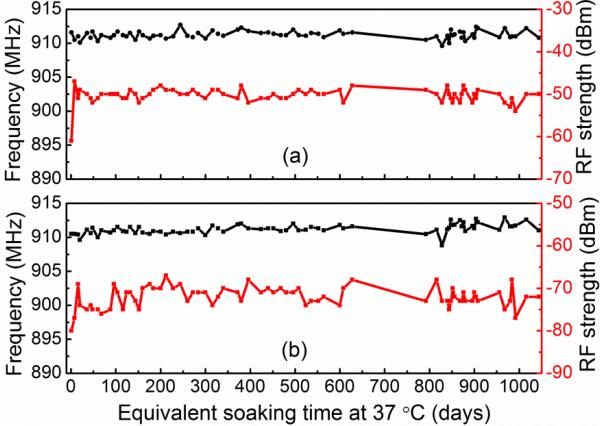
The long-term RF signal strengths and their corresponding frequencies are presented in Fig 8 as a function of soak time. The power-up frequencies were continuously near 910 MHz and the RF signal strengths were stably around -73 dBm (Fig 8 (b)) during the equivalent soaking time of 1044 days at 37 °C. The small fluctuations in RF signal strengths and respective frequencies could be caused by environmental noise and the different positions and distances between the reference wire and antenna. This represents a considerably longer soak testing results compared with Sharma et al.'s reporting of a lifetime of 276 days at room temperature using Parylene as encapsulation [57]. The room temperature soak testing is considered as a “decelerated” lifetime testing with aging factor of 0.35, which gave an equivalent lifetime of 100 days at 37 °C. The bilayer coated devices are still under soak testing. The long-term stability of power-up frequencies and RF signal strengths of the device implied the good insulation of the alumina and Parylene C bilayer encapsulation for biomedical implantable devices.
Fig 8.
Transmitted wireless RF signal strengths and frequencies monitored as a function of soak time in PBS. (a) Peak RF signal strengths and the respective frequencies as extracted from the spectra measured using a customized wireless hand receiver unit. (b) RF signal strengths and the respective frequencies as monitored from a spectrum analyzer. In both measurement methods, the RF signal strengths and corresponding frequencies stayed relatively stable during the 1044 days of equivalent soak time at 37 °C.
4.3 Active Arrays
Increasing current draw from these devices is a reliable indicator of encapsulation degradation and failure, and one of the dominant failure modes for the devices. The active arrays were powered up by a pair of 1.5 V batteries through wire-bonded gold wires. Vdd and Vss were both 1.5 V away from a common ground potential. The relatively high voltages (± 1.5 VDC) are more likely to accelerate electrochemical reactions and degradation modes. The current draw of Vdd and Vss was measured through a current meter, and was stable at ~3 mA (similar to current draw in air) for both Idd (from Vdd) and Iss (from Vss) during the 228 equivalent days of soak testing at 37 °C, as shown in Table 3. Also, all the 96 channels of the neural interface had good recording fidelity. This is a significant improvement over Parylene-only encapsulated active arrays, which typically last only 50 to 100 days under soak testing. The device was later used for in-vivo experiments. The low but constant current draw of the active arrays suggests the good encapsulation performance of alumina and Parylene coating because failure of encapsulation would induce high current draw due to the formation of leakage current paths and electrochemical corrosion processes.
Table 3.
Current draw of active array measured from Vdd and Vss as a function of soak time at 37 °C in PBS. The current draw was stable at ~ 3 mA for Idd and Iss from Vdd and Vss, respectively.
| Soak time | Idd (mA) | Iss (mA) |
|---|---|---|
| 0 (Agarose) | 2.9 | 2.9 |
| 1 day | 2.8 | 2.8 |
| 140 days | 3.0 | 2.9 |
| 228 days | 3.1 | 2.9 |
5 Conclusion
In summary, we have demonstrated the long-term reliability of ALD alumina and Parylene C bilayer coated neural interfaces from three different aspects: impedance, RF signal stability and strength, and current draw, which are all directly affected by the encapsulation performance. Wired, wireless UEAs and active arrays were soaked in PBS at 57 °C for accelerated lifetime testing. Different from the trend of continuous drop in impedance for Parylene-only coated arrays, median impedances of alumina and Parylene bilayer coated wired arrays increased from 60 kΩ to 160 kΩ after 960 equivalent days of soak testing at 37 °C. For bilayer coated arrays, the loss of iridium oxide and etching of silicon in PBS solution (leading to impedance increase) dominates over the slow bilayer encapsulation degradation (resulting in decreased impedance). Bilayer coated wireless UEAs incorporated with active electronics had stable power-up frequencies of ~ 910 MHz and constant RF signal strengths of ~ -50 dBm (measured by hand receiver) over 1044 equivalent days of soak testing at 37 °C, showing the slow water ingress and excellent insulation performance of the bilayer encapsulation. The current draw of active arrays was constant at ~ 3 mA with power supply of Vdd at 1.5 V and Vss at –1.5 V during 228 equivalent days of soak testing at 37 °C. The low and constant current draw is a reliable indication of good protection of the device by the encapsulation. Based on the coating performance on neural interfaces, it is believed that this bilayer encapsulation can be used for many other chronic biomedical implantable devices to improve their lifetime.
Acknowledgements
The authors would like to thank Fraunhofer IZM for the integration of the wireless devices. Funding of this research is provided by DARPA contract No: N66001-06-C-4056 and NIH contract No: 1R01NS064318-01A1. Sandeep Negi and Florian Solzbacher have financial interest in Blackrock microsystems, which develops and produces implantable neural interfaces. The views expressed are those of the authors and do not reflect the official policy or position of the Department of Defense or the U.S. Government. Approved for public release; distribution unlimited.
Contributor Information
Xianzong Xie, University of Utah, Department of Electrical and Computer Engineering.
Loren Rieth, University of Utah, Department of Electrical and Computer Engineering.
Layne Williams, Balckrock Microsystems.
Sandeep Negi, University of Utah, Department of Electrical and Computer Engineering.
Rajmohan Bhandari, University of Utah, Department of Electrical and Computer Engineering.
Ryan Caldwell, University of Utah.
Rohit Sharma, University of Utah.
Prashant Tathireddy, University of Utah, Department of Electrical and Computer Engineering.
Florian Solzbacher, University of Utah, Department of Electrical and Computer Engineering; University of Utah, Department of Bioengineering.
References
- 1.Hochberg LR, Serruya MD, Friehs GM, Mukand JA, Saleh M, Caplan AH, et al. Neuronal ensemble control of prosthetic devices by a human with tetraplegia. Nature. 2006;442:164–171. doi: 10.1038/nature04970. [DOI] [PubMed] [Google Scholar]
- 2.Donoghue JP. Connecting cortex to machines: Recent advances in brain interfaces. Nature Neuroscience. 2002;5:1085–1088. doi: 10.1038/nn947. [DOI] [PubMed] [Google Scholar]
- 3.Santhanam G, Ryu SI, Yu BM, Afshar A, Shenoy KV. A high-performance brain-computer interface. Nature. 2006;442:195–198. doi: 10.1038/nature04968. [DOI] [PubMed] [Google Scholar]
- 4.Wessberg J, Stambaugh CR, Kralik JD, Beck PD, Laubach M, Chapin JK, et al. Real-time prediction of hand trajectory by ensembles of cortical neurons in primates. Nature. 2000;408:361–365. doi: 10.1038/35042582. [DOI] [PubMed] [Google Scholar]
- 5.Normann RA. Technology Insight: Future neuroprosthetic therapies for disorders of the nervous system. Nature Clinical Practice Neurology. 2007;3:444–452. doi: 10.1038/ncpneuro0556. [DOI] [PubMed] [Google Scholar]
- 6.Velliste M, Perel S, Spalding MC, Whitford AS, Schwartz AB. Cortical control of a prosthetic arm for self-feeding. Nature. 2008;453:1098–1101. doi: 10.1038/nature06996. [DOI] [PubMed] [Google Scholar]
- 7.Rousche PJ, Normann RA. Chronic recording capability of the utah intracortical electrode array in cat sensory cortex. Journal of Neuroscience Methods. 1998;82:1–15. doi: 10.1016/s0165-0270(98)00031-4. [DOI] [PubMed] [Google Scholar]
- 8.Branner A, Stein RB, Normann RA. Selective stimulation and recording using a slanted multielectrode array. 1999:377. [Google Scholar]
- 9.Ledbetter NM, Ethier C, Oby ER, Hiatt SD, Wilder AM, Ko JH, Agnew SP, Miller LE, Clark GA. Intrafascicular stimulation of monkey arm nerves evokes coordinated grasp and sensory responses. Journal of Neurophysiology. 2013;109:580–590. doi: 10.1152/jn.00688.2011. [DOI] [PMC free article] [PubMed] [Google Scholar]
- 10.Biran R, Martin DC, Tresco PA. The brain tissue response to implanted silicon microelectrode arrays is increased when the device is tethered to the skull. Journal of Biomedical Materials Research Part A. 2007;82:169–178. doi: 10.1002/jbm.a.31138. [DOI] [PubMed] [Google Scholar]
- 11.Scott SH. Neuroscience: Converting thoughts into action. Nature. 2006;442:141–142. doi: 10.1038/442141a. [DOI] [PubMed] [Google Scholar]
- 12.Donoghue J. Comments on Tissue Response for BMI Elecrodes. presented at the 40th Neural Interfaces Conference; Salt Lake City, UT. 2012. [Google Scholar]
- 13.Yin M, Field R, Ghovanloo M. A 15-channel wireless neural recording system based on time division multiplexing of pulse width modulated signals. 2006:297–300. [Google Scholar]
- 14.Yin M, Ghovanloo M. Using pulse width modulation for wireless transmission of neural signals in multichannel neural recording systems. IEEE Transactions on Neural Systems and Rehabilitation Engineering. 2009;17:354–363. doi: 10.1109/TNSRE.2009.2023302. [DOI] [PMC free article] [PubMed] [Google Scholar]
- 15.Wise KD, Anderson DJ, Hetke JF, Kipke DR, Najafi K. Wireless implantable microsystems: High-density electronic interfaces to the nervous system. Proceedings of the IEEE. 2004;92:76–97. [Google Scholar]
- 16.Harrison RR, Kier RJ, Chestek CA, Gilja V, Nuyujukian P, Ryu S, Greger B, Solzbacher F, Shenoy KV. Wireless neural recording with single low-power integrated circuit. IEEE Transactions on Neural Systems and Rehabilitation Engineering. 2009;17:322–329. doi: 10.1109/TNSRE.2009.2023298. [DOI] [PMC free article] [PubMed] [Google Scholar]
- 17.Chestek CA, Gilja V, Nuyujukian P, Kier RJ, Solzbacher F, Ryu SI, Harrison RR, Shenoy KV. HermesC: Low-power wireless neural recording system for freely moving primates. IEEE Transactions on Neural Systems and Rehabilitation Engineering. 2009;17:330–338. doi: 10.1109/TNSRE.2009.2023293. [DOI] [PubMed] [Google Scholar]
- 18.Kim S, Bhandari R, Klein M, Negi S, Rieth L, Tathireddy P, Toepper M, Oppermann H, Solzbacher F. Integrated wireless neural interface based on the Utah electrode array. Biomedical microdevices. 2009;11:453–466. doi: 10.1007/s10544-008-9251-y. [DOI] [PubMed] [Google Scholar]
- 19.Dawes C. Laser welding: a practical guide. Woodhead Publishing; Cambridge, England: 1992. [Google Scholar]
- 20.Lago N, Ceballos D, Rodríguez FJ, Stieglitz T, Navarro X. Long term assessment of axonal regeneration through polyimide regenerative electrodes to interface the peripheral nerve. Biomaterials. 2005;26:2021–2031. doi: 10.1016/j.biomaterials.2004.06.025. [DOI] [PubMed] [Google Scholar]
- 21.Loeb GE, Bak MJ, Salcman M, Schmidt EM. Parylene as a chronically stable, reproducible microelectrode insulator. IEEE Transactions on Biomedical Engineering. 1977;24:121–128. doi: 10.1109/TBME.1977.326115. [DOI] [PubMed] [Google Scholar]
- 22.Hsu JM, Rieth L, Normann RA, Tathireddy P, Solzbacher F. Encapsulation of an integrated neural interface device with Parylene C. Biomedical Engineering, IEEE Transactions on. 2009;56:23–29. doi: 10.1109/TBME.2008.2002155. [DOI] [PubMed] [Google Scholar]
- 23.Wu J, Pike RT, Wong CP, Kim NP, Tanielian MH. Evaluation and characterization of reliable non-hermetic conformal coatings for microelectromechanical system (MEMS) device encapsulation. IEEE Transactions on Advanced Packaging. 2000;23:721–728. [Google Scholar]
- 24.Hsu JM, Tathireddy P, Rieth L, Normann AR, Solzbacher F. Characterization of a-SiCx: H thin films as an encapsulation material for integrated silicon based neural interface devices. Thin solid films. 2007;516:34–41. doi: 10.1016/j.tsf.2007.04.050. [DOI] [PMC free article] [PubMed] [Google Scholar]
- 25.Cogan SF, Edell DJ, Guzelian AA, Ping Liu Y, Edell R. Plasma-enhanced chemical vapor deposited silicon carbide as an implantable dielectric coating. Journal of Biomedical Materials Research Part A. 2003;67A:856–867. doi: 10.1002/jbm.a.10152. [DOI] [PubMed] [Google Scholar]
- 26.Roy RK, Lee KR. Biomedical applications of diamond-like carbon coatings: A review. Journal of Biomedical Materials Research - Part B Applied Biomaterials. 2007;83:72–84. doi: 10.1002/jbm.b.30768. [DOI] [PubMed] [Google Scholar]
- 27.Seymour JP, Elkasabi YM, Chen HY, Lahann J, Kipke DR. The insulation performance of reactive parylene films in implantable electronic devices. Biomaterials. 2009;30:6158–6167. doi: 10.1016/j.biomaterials.2009.07.061. [DOI] [PMC free article] [PubMed] [Google Scholar]
- 28.Hassler C, von Metzen RP, Ruther P, Stieglitz T. Characterization of parylene C as an encapsulation material for implanted neural prostheses. Journal of Biomedical Materials Research Part B: Applied Biomaterials. 2010;93:266–274. doi: 10.1002/jbm.b.31584. [DOI] [PubMed] [Google Scholar]
- 29.Xie XZ, Rieth L, Tathireddy P, Solzbacher F. Long-term in-vivo Investigation of Parylene-C as Encapsulation Material for Neural Interfaces. Procedia Engineering. 2011;25:483–486. [Google Scholar]
- 30.Guenther M, Gerlach G, Wallmersperger T, Avula MN, Cho SH, Xie X, et al. Smart Hydrogel-Based Biochemical Microsensor Array for Medical Diagnostics. Advances in Science and Technology. 2013;85:47–52. [Google Scholar]
- 31.Fortin JB, Lu TM. Chemical vapor deposition polymerization: the growth and properties of parylene thin films. Springer; Norwell, Massachusetts: 2004. [Google Scholar]
- 32.Licari JJ. Coating Materials for Electronic Applications - Polymers, Processes, Reliability, Testing. William Andrew Publishing/Noyes; Norwich, New York: 2003. [Google Scholar]
- 33.Szwarc M. Poly-para-xylelene: Its chemistry and application in coating technology. Polymer Engineering and Science. 1976;16:473–479. [Google Scholar]
- 34.Kane SR, Cogan SF, Ehrlich J, Plante TD, McCreery DB, Troyk PR. Electrical Performance of Penetrating Microelectrodes Chronically Implanted in Cat Cortex. Biomedical Engineering, IEEE Transactions on. 2013;60:2153–2160. doi: 10.1109/TBME.2013.2248152. [DOI] [PMC free article] [PubMed] [Google Scholar]
- 35.Li W, Rodger DC, Menon P, Tai YC. Corrosion Behavior of Parylene-Metal-Parylene Thin Films in Saline. ECS Transactions. 2008;11:1–6. [Google Scholar]
- 36.Ghosh A, Gerenser L, Jarman C, Fornalik J. Thin-film encapsulation of organic light-emitting devices. Applied physics letters. 2005;86:223503, 1–3. [Google Scholar]
- 37.Langereis E, Creatore M, Heil S, Van de Sanden M, Kessels W. Plasma-assisted atomic layer deposition of Al2O3 moisture permeation barriers on polymers. Applied physics letters. 2006;89:081915–081915-3. [Google Scholar]
- 38.Ferrari S, Perissinotti F, Peron E, Fumagalli L, Natali D, Sampietro M. Atomic layer deposited Al2O3 as a capping layer for polymer based transistors. Organic electronics. 2007;8:407–414. [Google Scholar]
- 39.Carcia PF, McLean RS, Reilly MH, Groner MD, George SM. Ca test of Al 2O 3 gas diffusion barriers grown by atomic layer deposition on polymers. Applied physics letters. 2006;89:031915, 1–3. [Google Scholar]
- 40.Potts S, Schmalz L, Fenker M, Díaz B, Światowska J, Maurice V, et al. Ultra-Thin Aluminium Oxide Films Deposited by Plasma-Enhanced Atomic Layer Deposition for Corrosion Protection. Journal of The Electrochemical Society. 2011;158:C132–C138. [Google Scholar]
- 41.Xie X, Rieth L, Merugu S, Tathireddy P, Solzbacher F. Plasma-assisted atomic layer deposition of Al2O3 and parylene C bi-layer encapsulation for chronic implantable electronics. Applied physics letters. 2012;101:093702, 1–5. doi: 10.1063/1.4748322. [DOI] [PMC free article] [PubMed] [Google Scholar]
- 42.Xie X, Rieth L, Caldwell R, Diwekar M, Tathireddy P, Sharma R, Solzbacher F. Long-Term Bilayer Encapsulation Performance of Atomic Layer Deposited Al2O3 and Parylene C for Biomedical Implantable Devices. Biomedical Engineering, IEEE Transactions on. 2013;60:2943–2951. doi: 10.1109/TBME.2013.2266542. [DOI] [PubMed] [Google Scholar]
- 43.Minnikanti S, Diao G, Pancrazio JJ, Xie X, Rieth L, Solzbacher F, Peixoto N. Lifetime assessment of atomic-layer-deposited Al2O3–Parylene C bilayer coating for neural interfaces using accelerated age testing and electrochemical characterization. Acta Biomaterialia. 2014;10:960–967. doi: 10.1016/j.actbio.2013.10.031. [DOI] [PubMed] [Google Scholar]
- 44.Campbell PK, Jones KE, Huber RJ, Horch KW, Normann RA. A silicon-based, three-dimensional neural interface: Manufacturing processes for an intracortical electrode array. IEEE Transactions on Biomedical Engineering. 1991;38:758–768. doi: 10.1109/10.83588. [DOI] [PubMed] [Google Scholar]
- 45.Bhandari R, Negi S, Rieth L, Solzbacher F. A wafer-scale etching technique for high aspect ratio implantable MEMS structures. Sensors and Actuators, A: Physical. 2010;162:130–136. doi: 10.1016/j.sna.2010.06.011. [DOI] [PMC free article] [PubMed] [Google Scholar]
- 46.Harrison RR, Kier RJ, Kim S, Rieth L, Warren DJ, Ledbetter NM, et al. A wireless neural interface for chronic recording. Biomedical Circuits and Systems Conference; Baltimore, MD. 2008.pp. 125–128. [Google Scholar]
- 47.Kim S, Harrison R, Solzbacher F. Influence of system integration and packaging for a wireless neural interface on its wireless powering performance. 2008:3182–3185. doi: 10.1109/IEMBS.2008.4649880. [DOI] [PubMed] [Google Scholar]
- 48.Rieth L, Franklin R, Tathireddy P, Sharma R, Williams L, Tenore F, et al. High channel-count neural interfaces for multiple degree-of-freedom neuroprosthetics. Procedia Engineering. 2011;25:1365–1368. [Google Scholar]
- 49.Xie X, Rieth L, Tathireddy P, Solzbacher F. Atomic layer deposited Al2O3 and parylene C dual-layer encapsulation for biomedical implantable devices. Solid-State Sensors, Actuators and Microsystems (TRANSDUCERS & EUROSENSORS XXVII), 2013 Transducers & Eurosensors XXVII: The 17th International Conference on; 2013.pp. 1044–1047. [Google Scholar]
- 50.Xie X, Rieth L, Cardwell R, Sharma R, Yoo JM, Diweka M, Tathireddy P, Solzbacher F. Bi-layer encapsulation of utah array based nerual interfaces by atomic layer deposited Al2O3 and parylene C. Solid-State Sensors, Actuators and Microsystems (TRANSDUCERS & EUROSENSORS XXVII), 2013 Transducers & Eurosensors XXVII: The 17th International Conference on; 2013.pp. 1267–1270. [Google Scholar]
- 51.Xie X, Rieth L, Negi S, Bhandari R, Diwekar M, Caldwell R, Sharma R, Tathireddy P, Solzbacher F. Self Aligned Tip Deinsulation of Atomic Layer Deposited Al2O3 and Parylene C Coated Utah Electrode Array Based Neural Interfaces. Journal of Micromechanics and Microengineering. 2014 doi: 10.1088/0960-1317/24/3/035003. Accepted for publication. [DOI] [PMC free article] [PubMed] [Google Scholar]
- 52.Hemmerich K. General aging theory and simplified protocol for accelerated aging of medical devices. MEDICAL PLASTIC AND BIOMATERIALS. 1998;5:16–23. [Google Scholar]
- 53.Hukins D, Mahomed A, Kukureka S. Medical. 2008;30:1270–1274. doi: 10.1016/j.medengphy.2008.06.001. [DOI] [PubMed] [Google Scholar]
- 54.Gunalan K, Warren DJ, Perry JD, Normann RA, Clark GA. An automated system for measuring tip impedance and among-electrode shunting in high-electrode count microelectrode arrays. Journal of Neuroscience Methods. 2009;178:263–269. doi: 10.1016/j.jneumeth.2008.12.020. [DOI] [PubMed] [Google Scholar]
- 55.Kane SR, Cogan SF, Ehrlich J, Plante TD, McCreery DB. Electrical performance of penetrating microelectrodes chronically implanted in cat cortex. 2011:5416–5419. doi: 10.1109/IEMBS.2011.6091339. [DOI] [PMC free article] [PubMed] [Google Scholar]
- 56.Vanhoestenberghe A, Donaldson N. Corrosion of silicon integrated circuits and lifetime predictions in implantable electronic devices. Journal of Neural Engineering. 2013;10 doi: 10.1088/1741-2560/10/3/031002. [DOI] [PubMed] [Google Scholar]
- 57.Sharma A, Rieth L, Tathireddy P, Harrison R, Oppermann H, Klein M, et al. Long term in vitro functional stability and recording longevity of fully integrated wireless neural interfaces based on the Utah Slant Electrode Array. Journal of Neural Engineering. 2011;8 doi: 10.1088/1741-2560/8/4/045004. [DOI] [PMC free article] [PubMed] [Google Scholar]


