Abstract
We investigate Second Harmonic Generation (SHG) in monolayer WS2 both deposited on a SiO2/Si substrate or suspended using transmission electron microscopy grids. We find unusually large second order nonlinear susceptibility, with an estimated value of deff ~ 4.5 nm/V nearly three orders of magnitude larger than other common nonlinear crystals. In order to quantitatively characterize the nonlinear susceptibility of two-dimensional (2D) materials, we have developed a formalism to model SHG based on the Green's function with a 2D nonlinear sheet source. In addition, polarized SHG is demonstrated as a useful method to probe the structural symmetry and crystal orientation of 2D materials. To understand the large second order nonlinear susceptibility of monolayer WS2, density functional theory based calculation is performed. Our analysis suggests the origin of the large nonlinear susceptibility in resonance enhancement and a large joint density of states, and yields an estimate of the nonlinear susceptibility value deff = 0.77 nm/V for monolayer WS2, which shows good order-of-magnitude agreement with the experimental result.
Two-dimensional (2D) materials, exhibiting extraordinary and novel properties not available in their bulk forms, are at the forefront of nanomaterial technologies1,2,3,4,5,6,7,8. For instance, the transition metal dichalcogenide (TMD) family of monolayer materials (such as MoS2, WS2), unlike their bulk counterparts, possesses direct band gaps9,10,11,12 and could thus generate strong photoluminescence13,14,15,16,17. The TMD family of monolayer materials have also garnered interest in nonlinear optics18,19. Characterization of exfoliated WS220 and synthesized MoS2 monolayers21,22,23 has revealed large second-order nonlinear susceptibility, as high as nm/V22,23. Here we investigate SHG in monolayer WS2 synthesized by chemical vapour deposition. We have developed a formalism to model SHG in 2D materials using the Green's function with a 2D nonlinear sheet source, which also takes into account the focused excitation geometry and the substrate effect as opposed to a simple plane-wave model. SHG in WS2 monolayers both suspended and deposited on SiO2/Si substrates is studied. The estimated second order nonlinear susceptibility is approximately three orders of magnitude higher than that of common nonlinear optical crystals such as BBO24. Polarized SHG in WS2 is studied to probe the tensorial nonlinear susceptibility, which is related to the structural symmetry of the 2D crystal. To gain further insight into the large nonlinear susceptibility, density functional theory (DFT) calculations of the second-order nonlinear susceptibility are also performed.
Results
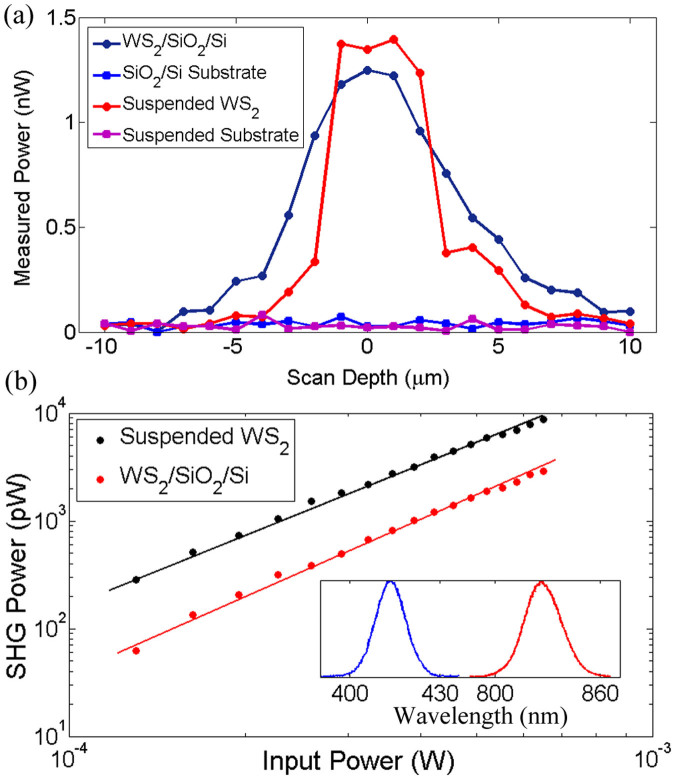
A WS2 monolayer lacks inversion symmetry and has non-vanishing second-order nonlinear susceptibility. An experimental setup was developed to characterize the SHG in the synthesized WS2 samples (Fig. 1a). Fig. 1(b) shows an optical micrograph of a triangular monolayer of WS2 grown on a SiO2/Si substrate. The same triangle is also shown as an SHG image in Fig. 1(c), obtained by raster scanning the sample with a step size of 1 μm. As can be observed from the SHG image, the background contribution from the substrate surface in the surrounding area is negligible. To further isolate substrate effects, the same experiments were also performed on a WS2 sample that was suspended on a transmission electron microscopy (TEM) grid. Fig. 1(d) shows an optical micrograph of the WS2 film on the TEM grid, and Fig. 1(e) shows the SHG image of the same triangle. Although the WS2 triangle can barely be seen on the TEM grid micrograph due to weak reflection contrast, the triangle is easily apparent in the SHG image. A depth scan was also performed on the WS2 samples and bare substrates to measure the SHG signal as a function of sample depth position, by translating the sample axially with a computer-controlled linear stage. The results shown in Fig. 2(a) indicate that the Second Harmonic (SH) signals generated from both the on-substrate and suspended samples are predominantly from the WS2 monolayers, as the bare substrates had no detectable SH signal under the same measurement conditions. To characterize the second-order nonlinear susceptibility, we measured the average power of the SHG signal as the power of the fundamental beam was varied. Fig. 2(b) shows that the resulting relation is quadratic: a linear fit of the log-log plot reveals a slope of 2.04 for the TEM-suspended WS2 sample, and 2.12 for the WS2/SiO2/Si substrate sample. The lower inset of Fig. 2(b) shows representative spectra of the fundamental and SHG signal, which also clearly indicate the frequency doubling.
Figure 1.
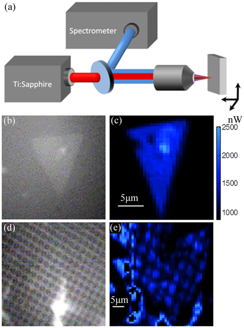
(a) Schematic diagram of the experimental setup for characterizing SHG in WS2 monolayers. The fundamental beam is from a mode-locked Ti:sapphire laser (832 nm center wavelength, 88 MHz repetition rate) and the second harmonic signal generated by the WS2 monolayer is epi-collected and measured using a spectrometer. (b) Optical micrograph of a synthesized triangular WS2 monolayer grown on a SiO2/Si substrate. (c) SHG image of the same WS2 triangle obtained by raster scanning the sample. (d) Optical micrograph of a synthesized triangular WS2 monolayer placed on a transmission electron microscopy grid. (e) SHG image of the same WS2 triangle obtained by raster scanning the sample.
Figure 2.
(a) SHG scan with sample translated along the axial direction. The distance is relative to the surface of the substrate. The vertical axis shows the SH signals generated from WS2 on a SiO2/Si substrate (average incident power = 1 mW) and suspended on a TEM grid (average incident power = 0.7 mW), as well as SH signals for the bare SiO2/Si substrate and TEM grid, by focusing the fundamental beam to different depths. There is no detectable SHG signal from the bare substrate without the WS2 triangular monolayer, thus allowing all the SH signal generated at the surface of the sample to be attributed to the presence of WS2. (b) Power dependence of the SH signal generated from a triangular WS2 monolayer in a logarithmic scale on both the suspended and the SiO2/Si substrate. The measured power is shown as points and the linear fit is plotted as a solid line. The bottom inset shows the normalized fundamental laser spectrum and a typical normalized spectrum of the SH signal generated from a WS2 monolayer.
Discussion
In order to quantitatively characterize the second-order nonlinear susceptibility, we have developed a formalism to model SHG from 2D materials on a semi-infinite substrate. A plane-wave fundamental beam uniformly filling the aperture of a lens (focal length F, aperture radius a, numerical aperture NA = a/F) is focused onto the 2D material, and the generated SH signal is epi-collected. The fundamental field at the sample can be represented by the Debye integral25
 , where E10 represents the incident field at the lens aperture, n1 is the refractive index of the substrate at the fundamental wavelength λ1, and circ() is the circular aperture function. The paraxial approximation is used, and the Fresnel coefficient for normal incidence is also taken into account. The SHG is governed by the wave equation
  , where E2 is the complex SH field,
  and
and  represent the polarization of the fundamental and SH beam, ω2 is SH angular frequency, c is the speed of light in vacuum, ε0 and μ0 are the vacuum permittivity and permeability, and χ(2) is the second-order nonlinear susceptibility tensor19. Due to its atomic thickness, the nonlinear susceptibility of the 2D material can be modelled by a Dirac delta function with an effective surface nonlinear susceptibility, i.e.
  . Additionally, n(z) = 1 (z < 0) or n2(z > 0), the refractive index of the substrate at the SH frequency. The SHG from the substrate surface is neglected, as justified by the experimental observation of no signal for the substrate background measurements of Fig. 1(c) and Fig. 2(a).
The relationship between the fundamental excitation power P1 and the SH signal power P2 is obtained by solving for the Green's function with the nonlinear sheet source:
 |
with  .
.
From Eq. (1) we can express the surface nonlinear susceptibility in terms of the average power, the pulse width, and the pulse repetition rate:
 |
where R is the repetition rate, ti is the pulse width, and Pavi is the average power (i = 1: fundamental, 2: SH). Since the WS2 monolayer has atomic thickness much shorter than the pulse length involved, the continuous wave approximation is still valid even though chirped femtosecond pulses are used in our experiment. In our calculation, the instantaneous power of the fundamental beam is approximated by the pulse energy divided by the pulse duration time. The calculated nonlinear susceptibility represents an averaged value over the pulse bandwidth. Based on data taken similar to that of Fig. 2(b) (from 30 triangles on 3 separate substrates) and Eq. (2), the effective bulk-like second-order susceptibility of the grown WS2 monolayers, with  where T = 0.65 nm is the thickness of a WS2 monolayer, was estimated to be 4.46 nm/V for the suspended film with a standard deviation of 0.09 nm/V across all samples, and 4.51 nm/V for the WS2 triangle on a SiO2/Si substrate with a standard deviation of 0.55 nm/V. Note that the standard deviations should be interpreted as the consistency of the measured SHG power rather than the accuracy of the susceptibility value due to the assumptions that were made in our calculation. These estimated values are nearly three orders of magnitude greater than that of typical nonlinear crystals24. It should also be noted that the SiO2/Si substrate may not be simply treated as a semi-infinite homogeneous medium due to the presence of the SiO2/Si interface, as it is well known such substrate has contrast enhancement26. The calculated nonlinear susceptibility thus needs to be adjusted by an enhancement factor, i.e.,
  where η1 and η2 are the field enhancement factors for the fundamental and the epi-detected SH field, respectively, due to the Fabry-Perot cavity formed by air/SiO2 and SiO2/Si interfaces.
  is the calculated value using Eq. (2), and
  is the actual nonlinear susceptibility. For a substrate with 300 nm of SiO2 above silicon, the susceptibility value is estimated to be 15% more when the cavity enhancement factors are accounted. This analysis of the enhancement factor assumes a normally incident plane wave. A more rigorous approach would require angular spectrum decomposition of the incident wave. For this reason, the suspended sample is likely to yield a better estimate of the nonlinear susceptibility.
In addition to the value of deff, the tensorial property of the second-order nonlinear susceptibility of WS2 monolayers can also be probed by polarized SHG. The WS2 monolayer has P63/mmc crystal symmetry, resulting in a second-order nonlinear susceptibility tensor with nonzero elements dyyy = −dyxx = −dxxy = −dxyx where x and y represent the crystal axes19. The polarized SH signal power P2 ∝ cos2 3θ where θ is the angle between the x crystal axis and the incidence polarization27. This relationship is shown compared to experimental results in Fig. (3). Two WS2 monolayer triangles on the same SiO2/Si substrate are shown by SHG raster scan. The two inserts are polar plots where the circles are measured data points and the solid line is the cos2 3θ fit. The two polar plots are rotated by 18 degrees with respect to each other, and the left edge of the two triangle SHG images appear to be rotated by a similar angle. The experimental data and theoretical curve agree well and clearly demonstrate six-fold symmetry. As the tensor structure of χ(2) is closely related to the symmetry of the material structure, polarized SHG can be a useful tool for probing the structural symmetry of 2D materials.
Figure 3. Polarized SHG in WS2 triangles.
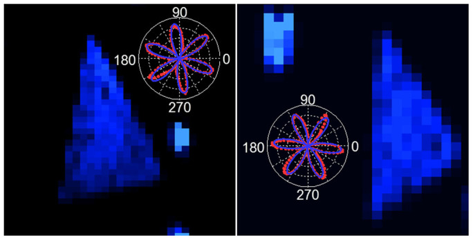
The SHG images show two monolayer WS2 triangles on the same SiO2/Si substrate. The polar plots show the normalized polarization dependence of SHG in WS2 monolayer islands. Dots are measured data and the solid curves are the theoretical fit. The two polar plots reveal a rotation of 18 degrees between the two triangles.
To understand the origin of the giant experimentally observed second-order nonlinearity we have also calculated the second-order nonlinear optical susceptibility of monolayer WS2 at the level of density functional theory (DFT), extending beyond existing literature results in the tight binding approximation28. Note that the band gap measured by photoluminescence agrees with the DFT calculation surprisingly well, due to the partial cancellation of quasi-particle effects and exciton binding29. On the other hand, calculations at the quasi-particle or Bethe-Salpeter equation level are computationally expensive, due to the very fine k-point mesh required. For an accurate description of the second-order response we follow the formalism of Sipe and Ghahramani30,31,32,33 as implemented in the ABINIT package34,35, including both inter-band transitions and intra-band currents. Although completely filled bands produce no intra-band current at the linear order, intra-band motion does occur at second order30,32. The ground-state properties and response functions were calculated within the local density approximation35 using norm-conserving pseudopotentials with an energy cut-off of 760 eV and a k-point mesh of 69 × 69 × 1 within ABINIT36,37,38,39,40. The optical spectra achieved convergence with 50 conduction bands and a smearing of 15 meV.
The band structure of monolayer WS2 features three nearly parallel bands along Γ-K, as shown by the shaded areas near II and IV in Fig. 4. The highest valence band is parallel to both the first and the second conduction bands, yielding two peaks labelled II and IV in jω the joint density of states (JDOS) of Fig. 5. Another prominent feature in the JDOS, labelled V, originates from transitions near the K point. The second-order interband transition V could be strongly enhanced by the intermediate transition I at the half-way point in energy, if these matrix elements are non-vanishing. This is confirmed by the calculated nonlinear spectra.
Figure 4. The band structure of monolayer WS2.
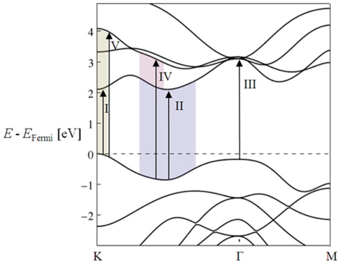
The parallel bands along Γ-K give rise to maxima in the joint density of states.
Figure 5. The nonlinear susceptibility χ(2) of monolayer WS2.
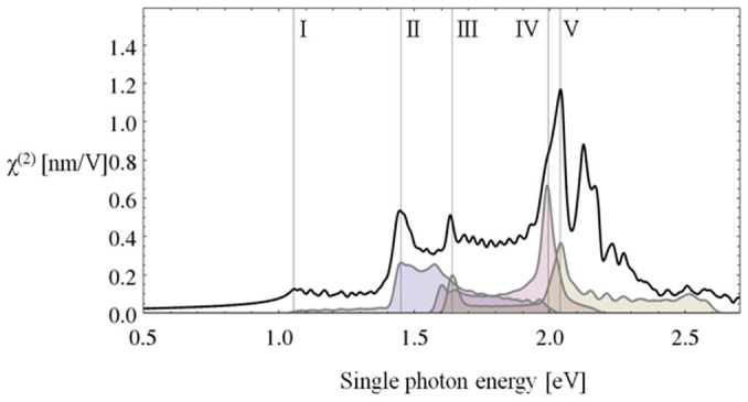
Also shown is the colour-coded joint density states contributions from the highest valence band to the first, second, and third conduction bands, aligned to the calculated spectra at the appropriate second-order resonant frequencies and following the colour scheme of Fig. 4.
In addition to the calculated χ(2), Fig. 5 also shows the JDOS, horizontally rescaled to j(2ω) to match resonances arising from the 2ω terms and separated out by colour-coded destination bands following the same colour scheme as in Fig. 4. The main features in the JDOS match well with the calculated χ(2) spectra. Resonance I has the lowest excitation energy, corresponding to half the band gap. Resonances II and IV clearly benefit from a large JDOS. Resonance V arises from transitions near the K point, which lies at almost twice the band gap (also at K). Near transition II (corresponding to a wavelength of 832 nm) we obtain χ(2) = 0.5 nm/V. With the simulation cell height of 2 nm, we obtain a value of deff = 0.77 nm/V. The calculation confirms the very large non-linear response observed experimentally, and considering the overall magnitude of the effect and the neglect of quasiparticle and excitonic effects, the semi-quantitative agreement to experiment is surprisingly good.
In summary, we report strong SHG from synthesized WS2 monolayer islands both on SiO2/Si substrate and suspended on a TEM grid, as well as a theoretical calculation of the second-order susceptibility using DFT. In order to experimentally determine the second-order susceptibility of 2D materials, we have developed a SHG model based on the Green's function, yielding an estimated bulk-like second-order nonlinear susceptibility deff approximately 4.5 nm/V for a WS2 monolayer. In addition, by using polarized SHG, the crystal symmetry and orientation of the WS2 monolayer can be revealed, demonstrating SHG as a useful method to probe structural information in 2D materials. Further analysis through DFT calculations indicate that the large second-order susceptibility is due to resonance enhancement as well as the large joint density of states. Despite the approximations involved, the calculated nonlinear susceptibility (deff = 0.77 nm/V) using DFT shows reasonable order-of-magnitude agreement with the experimental result. With giant χ(2) and sub-nanometre thickness, the integration of 2D TMD materials with photonic circuits to realize new nonlinear optical devices could be a fertile ground worth further exploration.
Methods
Synthesis
The WS2 triangle monolayer samples were grown on SiO2/Si substrates using a two-step process17. Briefly, one-nm films of WO3 (99.998%, Alfa Aesar) were thermally evaporated onto a SiO2/Si substrate at 10−6 Torr. The films were placed into a quartz reaction tube next to a boat containing sulphur powder (99.5%, Alfa Aesar). The sulphur zone was heated up to 250°C and the furnace where the WO3 sample was located was heated to 800°C. The synthesis was carried out in an inert environment under an Ar flow using 100 sccm and atmospheric pressure at the outlet. To verify the structural quality and integrity of the grown WS2 monolayers, Raman spectroscopy using a Renishaw inVia micro-Raman was carried out at 514.5 nm laser excitation. The 2LA(M) phonon mode (352 cm−1) had an intensity twice as high as that of the A1g mode (418 cm−1), which, according to reference 41, is a characteristic of monolayer WS2, thus confirming that the synthesized WS2 samples are indeed monolayers.
Characterization
The output from a mode-locked Ti:sapphire laser (from KM Labs with centre wavelength of 832 nm and repetition rate of 88 MHz) was filtered, attenuated, and focused onto a sample by a long-working-distance objective lens (Mitutoyo 50×, NA = 0.55, spot size ~ 1.8 μm at fundamental wavelength). The generated SH signal was then back collected by the same lens, separated using a dichroic mirror, and filtered by a 405 nm bandpass filter before entering a spectrometer (PI Acton 2500i with a liquid nitrogen cooled charge coupled device − CCD camera). The signal value of the spectrometer was calibrated using an attenuated (by neutral density filters) SH signal separately generated from a BBO crystal with known power measured by a power meter (Newport 1830-C). In order to assist the alignment and ensure that the signal was collected from a WS2 monolayer island, an imaging system was co-set up so that a removable mirror could direct the image signal towards an imaging CCD camera. In addition, in order to calculate the susceptibility, the laser pulse width needs be known in situ, i.e. directly on the sample at the focal point of the objective lens. Therefore, we performed a collinear frequency resolved optical gating (cFROG) measurement42 by using the same WS2 sample to determine the pulse width (106 fs, chirped). Although there exists dispersion in the χ(2) of WS2 (c.f. fig. 5), with our laser's relatively narrow bandwidth of about 18 nm, this was determined not to be an issue and was confirmed by the agreement of the retrieved spectrum with the measured laser spectrum. WS2 monolayer may also enable the characterization of complex pulses with broad bandwidth if its susceptibility is pre-calibrated. To measure the polarization dependence, the fundamental beam was first prepared in a circular polarization state using a quarter-wave plate. A broadband polarizer was inserted between the objective lens and the dichroic mirror to serve as both the polarizer for projecting the input fundamental beam into a linear polarization state and the analyzer for the generated SHG signal. The polarizer was mounted on a computer-controlled rotational stage to continuously rotate its polarization axis.
Author Contributions
C.J., D.M. and N.M. performed SHG characterization and analysis. A.L.E. and N.P.L. synthesized samples. Y.W. performed DFT calculation. Z.L., M.T. and V.C. supervised the project.
Acknowledgments
The authors acknowledge the support from NSF MRSEC program under DMR 0820404. ZL acknowledges support from NSF award ECCS 0925591. ALE, NPL, and MT acknowledge support by the U. S. Army Research Office under MURI ALNOS project, contract/grant number W911NF-11-1-0362.
References
- Butler S. Z. et al. Progress, challenges, and opportunities in two-dimensional materials beyond graphene. ACS Nano. 7, 2898–2926 (2013). [DOI] [PubMed] [Google Scholar]
- Geim A. K. & Novoselov K. S. The rise of graphene. Nature Materials 6, 183–191 (2007). [DOI] [PubMed] [Google Scholar]
- Novoselov K. S. et al. Two-dimensional atomic crystals. Proc. Natl. Acad. Sci. U.S.A. 102, 10451 (2005). [DOI] [PMC free article] [PubMed] [Google Scholar]
- Ci L. et al. Atomic layers of hybridized boron nitride and graphene domains. Nat. Mat. 9, 430–435 (2010). [DOI] [PubMed] [Google Scholar]
- Osada M. et al. High-k dielectric nanofilms fabricated from titania nanosheets. Adv. Mater. 18, 1023–1027 (2006). [Google Scholar]
- Novoselov K. S. et al. Electric field effect in atomically thin carbon films. Science. 306, 666–669 (2004). [DOI] [PubMed] [Google Scholar]
- Kamihara Y., Watanabe T., Hirano M. & Hosono H. Iron-based layered superconductor La[O1−xFx]FeAs (x = 0.05–0.12) with Tc = 26 K. J. Am. Chem. Soc. 130, 3296–3297 (2008). [DOI] [PubMed] [Google Scholar]
- Takada K. et al. Superconductivity in two-dimensional CoO2 layers. Nature. 422, 53–55 (2003). [DOI] [PubMed] [Google Scholar]
- Coleman J. N. et al. Two-dimensional nanosheets produced by liquid exfoliation of layered materials. Science. 331, 568–571 (2011). [DOI] [PubMed] [Google Scholar]
- Mak K. F., Lee C., Hone J., Shan J. & Heinz T. F. Atomically thin MoS2: a new direct-gap semiconductor. Phys. Rev. Lett. 105, pp136805 (2010). [DOI] [PubMed] [Google Scholar]
- Zhao W. et al. Evolution of electronic structure in atomically thin sheets of WS2 and WSe2. ACS Nano. 7, 791–797 (2010). [DOI] [PubMed] [Google Scholar]
- Frey G. L., Tenne R., Matthews M. J., Dresselhaus M. S. & Dresselhaus G. Optical properties of MS2 (M 5 Mo, W) inorganic fullerene like and nanotube material optical absorption and resonance Raman measurements. J. Mater. Res. 13, 2412–2417 (1998). [Google Scholar]
- Splendiani A. et al. Emerging photoluminescence in monolayer MoS2. Nano Lett 10, 1271–1275 (2010). [DOI] [PubMed] [Google Scholar]
- Eda G. et al. Photoluminescence from chemically exfoliated MoS2. Nano Lett. 11, 5111–5116 (2011). [DOI] [PubMed] [Google Scholar]
- Wang Q. H., Kalantar-Zadeh K., Kis A., Coleman J. N. & Strano M. S. Electronics and optoelectronics of two-dimensional transition metal dichalcogenides. Nat. Nano. 7, 699–712 (2012). [DOI] [PubMed] [Google Scholar]
- Chen Y. et al. Tunable band gap photoluminescence from atomically thin transition-metal dichalcogenide alloys. ACS Nano. 7, 4610–4616 (2013). [DOI] [PubMed] [Google Scholar]
- Gutiérrez H. R. et al. Extraordinary room-temperature photoluminescence in WS2 triangular monolayers. Nano Lett. 13, 3447–3454 (2013). [DOI] [PubMed] [Google Scholar]
- Shen Y. R. Surface properties probed by second-harmonic and sum-frequency generation. Nature 337, 519–525 (1989). [Google Scholar]
- Robert B. Nonlinear Optics. (Academic Press, San Diego, 2003). [Google Scholar]
- Zeng H. et al. Optical signature of symmetry variations and spin-valley coupling in atomically thin tungsten dichalcogenides. Sci. Rep. 3, 1608 (2013). [DOI] [PMC free article] [PubMed] [Google Scholar]
- Malard L. M., Alencar T. V., Barboza A. P. M., Mak K. F. & de Paula A. M. Observation of intense second harmonic generation from MoS2 atomic crystals. Phys. Rev. B. 87, 201401 (2013). [Google Scholar]
- Li Y. et al. Probing symmetry properties of few-layer MoS2 and h-BN by optical second-harmonic generation. Nano Lett. 13, 3329–3333 (2013). [DOI] [PubMed] [Google Scholar]
- Wagoner G. A., Persans P. D., Van Wagenen E. A. & Korenowski G. M. Second-harmonic generation in molybdenum Disulfide. J. Opt. Soc. Am. B. 15, 1017–1021 (1998). [Google Scholar]
- Amnon Photonics. (Oxford University Press, New York, 2007). [Google Scholar]
- Born M. & Wolf E. Principles Of Optics. (Cambridge University Press. Cambridge, 1999). [Google Scholar]
- Benameur M. M., Radisavljevic B., Heron J. S., Sahoo S., Berger H. & Kis A. Visibility of dichalcogenide nanolayers. Nanotechnology 22, 125706 (2011). [DOI] [PubMed] [Google Scholar]
- Midwinter J. E. & Warner J. The effects of phase matching method and of uniaxial crystal symmetry on the polar distribution of second-order non-linear optical polarization. Bri. J. Appl. Phys. 16, 1135–1142 (1965). [Google Scholar]
- Trolle M. L., Seifert G. & Pedersen T. G. Theory of second harmonic generation in few-layered MoS2. (2013). http://arxiv.org/abs/1310.0674.
- Komsa H.-P. & Krasheninnikov A. V. Effects of confinement and environment on the electronic structure and exciton binding energy of MoS2 from first principles. Phys. Rev. B 86, 241201 (2012). [Google Scholar]
- Sipe J. E. & Ghahramani E. Nonlinear optical response of semiconductors in the independent-particle approximation. Phys. Rev. B 48, 11705–11722 (1993). [DOI] [PubMed] [Google Scholar]
- Hughes J. L. P. & Sipe J. E. Calculation of second-order optical response in semiconductors. Phys. Rev. B 53, 10751–10763 (1996). [DOI] [PubMed] [Google Scholar]
- Aversa C. & Sipe J. E. Nonlinear optical susceptibilities of semiconductors: Results arith a length-gauge analysis. Phys. Rev. B 52, 14636–14645 (1995). [DOI] [PubMed] [Google Scholar]
- Rashkeev S. N., Lambrecht S. N. & Segall B. Efficient ab initio method for the calculation of frequency-dependent second-order optical response in semiconductors. Phys. Rev. B 57, 3905–3919 (1998). [Google Scholar]
- Sharma S., Dewhurst J. K. & Ambrosch-Draxl C. Linear and second-order optical response of III-V monolayer superlattices. Phys. Rev. B 67, 165332 (2003). [Google Scholar]
- Sharma S. & Ambrosch-Draxl C. Second-Harmonic Optical Response from First Principles. Phys. Scr. 109, 128–134 (2004). [Google Scholar]
- Perdew J. P. & Zunger A. Self-interaction correction to density-functional approximations for many-electron systems. Phys. Rev. B 23, 5048–5079 (1981). [Google Scholar]
- Gonze X. et al. ABINIT: First-principles approach to material and nanosystem properties. Comput. Phys. Commun. 180, 2582–2615 (2009). [Google Scholar]
- Gonze X. et al. A brief introduction to the ABINIT software package. Z. Kristallogr. 220, 558–562 (2005). [Google Scholar]
- Gonze X. & Lee C. Dynamical matrices, Born effective charges, dielectric permittivity tensors, and interatomic force constants from density-functional perturbation theory. Phys. Rev. B 55, 10355–10268 (1997). [Google Scholar]
- Gonze X. First-principles responses of solids to atomic displacements and homogeneous electric fields: Implementation of a conjugate-gradient algorithm. Phys. Rev. B 55, 10337–10354 (1997). [Google Scholar]
- Berkdemir H. R. et al. Identification of individual and few layers of WS2 using Raman Spectroscopy. Sci. Report. 3, 1755 (2013). [Google Scholar]
- Amat-Roldán I., Cormack I. G., Loza-Alvarez P., Gualda E. J. & Artigas D. Ultrashort pulse characterization with SHG collinear-FROG. Opt. Exp. 12, 1169–1178 (2004). [DOI] [PubMed] [Google Scholar]


