Abstract
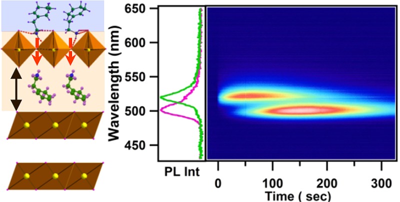
The properties of layered inorganic semiconductors can be manipulated by the insertion of foreign molecular species via a process known as intercalation. In the present study, we investigate the phenomenon of organic moiety (R-NH3I) intercalation in layered metal-halide (PbI2)-based inorganic semiconductors, leading to the formation of inorganic–organic (IO) perovskites [(R-NH3)2PbI4]. During this intercalation strong resonant exciton optical transitions are created, enabling study of the dynamics of this process. Simultaneous in situ photoluminescence (PL) and transmission measurements are used to track the structural and exciton evolution. On the basis of the experimental observations, a model is proposed which explains the process of IO perovskite formation during intercalation of the organic moiety through the inorganic semiconductor layers. The interplay between precursor film thickness and organic solution concentration/solvent highlights the role of van der Waals interactions between the layers, as well as the need for maintaining stoichiometry during intercalation. Nucleation and growth occurring during intercalation matches a Johnson–Mehl–Avrami–Kolmogorov model, with results fitting both ideal and nonideal cases.
Keywords: inorganic−organic perovskite thin films, natural multiple quantum wells, intercalation dynamics, room-temperature excitons
Introduction
Intercalation, the insertion of guest species into a host crystal, is an efficient route for generating new materials with novel properties. Some of the earliest and most extensive studies have involved the intercalation of nanocomponents such as dyes, nanotubes, and colloids into porous materials such as block copolymers, zeolites, and colloidal crystals.1,2 Three types of goal are sought: to cast a new material as a replica of the host, to store intercalates with high density as in lithium batteries, or to establish new material properties based on the novel layered superlattices formed. Although inorganic crystals offer distinct advantages such as high carrier mobility and thermal/mechanical stability, organic materials show structural tunability and are easily processable.3−7 Inorganic–organic (IO) hybrid materials are a unique class of materials that combine the useful properties of these two individual entities into a single molecular framework.
A distinct class of IO hybrid material that has emerged in the recent past are AMX3 type perovskites (A = organic moiety, M = Pb2+, Sn2+, etc., and X = I–, Br–, or Cl–) that are derived from the layered inorganic MX2 host network.8 These perovskites have been extensively studied for their structural, optical, electrical, thermochromic and other properties.9−13 The variation in their structural and optical features strongly depends on the extended network of MX6 octahedra. Depending on the size, shape, and functionality of organic cations, the 3D inorganic network is altered to form extended 2D layers (“wells”), 1D chains (“wires”), 0D (“isolated dots”), or other intermediate cases.14 On the basis of their inorganic network arrangement these IO hybrids show very different opto/electrical properties at room temperature to the base crystals. For example, the 3D inorganic “cage type” (CH3NH3)PbI3 and analogous hybrids show tremendous promise in photovoltaic research, producing devices with efficiencies of up to 15%.15−17 Similarly, for 2D layered perovskites, (C6H5C2H4NH3)2SnI4 based thin-film transistors (TFTs) show mobilities of ∼1 cm2/(V s) and (C6H5C2H4NH3)2PbI4 has been used in heterostructure electroluminescent (EL) devices with low-temperature luminance intensities of 10,000 cd/m2 at 24 V.18−20
For these materials, the parent inorganic MX2 consists of noninteracting extended 2D M-X networks, well-separated and with weak van der Waals interlayer forces. As a result, the insertion of guest organic moieties (mostly amine based) leads to a change in the physical properties (optical, electrical, morphological, etc.) of the host (parent) semiconductor.22,23 Recently we have reported the in situ dynamic evolution of exciton absorption when organic (C6H9C2H4NH3)I intercalates between PbI2 layers, yielding highly oriented layered perovskite thin films of (C6H9C2H4NH3)2PbI4.24 Similarly, the transformation of PbI2 into CH3NH3PbI3 has been monitored within a porous TiO2 film optimized for solar cell fabrication.17 In general, intercalation mechanisms have been studied previously using methods such as X-ray diffraction, Raman imaging and resistance measurements.25−27 The growth kinetics have been explained by various models, most notably the Johnson-Mehl-Avrami–Kolmogorov (JMAK) model.28−32 Recently, the kinetics of molecular intercalation in various layered materials (for example graphene, MoS2, VS2) have been studied using such models,25,33,34 and attention is being focused on understanding the intercalation of biologically active materials into layered double hydroxide hosts (LDHs).1,35
Among all perovskites, the 2D layered networks ((R-NH3)2MX4 type) are of special interest. These IO perovskites are considered to be self-assembled natural multiple quantum wells, made up of alternating layers of inorganic semiconducting monolayers and optically inert organic spacer moieties. In these hybrid materials, the bandgap of inorganic entity (∼2–3 eV) is specifically chosen to be less than the nonemitting organic counterpart (∼4–5 eV).8,20 Optically, these materials exhibit sharp resonances due to Mott–Wannier excitons confined within the semiconductor layers.20 As a result of the large dielectric mismatch between the inorganic and organic constituents (dielectric confinement), such excitons are observable at room temperature, with large binding energies (∼300 meV).20,21 The strong room-temperature excitonic features of 2D perovskites make them potential candidates for optoelectronic devices such as IO-LEDs (Inorganic–Organic Light Emitting Diodes), IO-FETs (inorganic–organic field-effect transistors), solar cells, nonlinear optical switches, and exciton-photon coupling structures.15−19,36 Conventionally, thin films of these perovskites are fabricated by spin coating the chemically synthesized components using an appropriate solvent. However, for practical device applications, precise control over film thickness, reproducibility, uniformity, and morphology is essential. Because of difficulties associated with solution processing methods, alternative fabrication of thin films from dual-boat vacuum deposition and electrochemical deposition have recently been explored.37−39 However, such deposition methods still encounter problems, such as maintaining stoichiometry by controlling the pressure and rate of evaporation (for dual-boat vacuum deposition), or controlling the dissociation ratios (in the case of electrochemical deposition). Therefore, to obtain higher-quality perovskite thin films, an optimized intercalation strategy would be highly advantageous.24 Moreover, highly ordered layering is essential for the observation of strong exciton features from these IO hybrids, which is strongly dependent on (1) the disorder and conformation of the organic moiety, (2) the crystal packing, (3) the structure of the inorganic layers, and (4) the position of the organic amine group attached to the M-X network. Understanding the intercalation process at a molecular level and how it varies with the type/size of organic moieties, optimizing parameters such as inorganic film thickness, is thus essential for the realization of well-ordered uniform device quality films. However, the mechanism of organic intercalation in 1D, 2D, or 3D hybrids, including nucleation and growth processes, intercalation directions, and induced conformation changes are complex, and no such efforts have been reported so far.
Here, we thus study the in situ evolution of organic intercalation into the PbI2 network. For the first time, the direction of intercalation is explored using optical probes. The intercalation process has been optimized for various organic moieties by controlling the thickness of the PbI2 film and the intercalation solvent/solution concentration, to obtain highly ordered 2D inorganic–organic perovskites of type (R-NH3)2PbI4. The evolution of strong optical excitons observed in these multiple quantum well systems are systematically monitored during the intercalation and key issues such as growth directions and the dynamics involved are considered using suitable models. Finally, ways to explain the molecular level changes that lead to the formation of device quality thin films are introduced.
Experimental Section
We have outlined the basic intercalation methodology in a recent communication,24 so fabrication is only briefly reviewed here. Layered parent PbI2 thin films of various thickness are deposited on glass substrates by thermal vapor deposition at ∼1 × 10⁻⁶ Torr. To obtain organic iodide (C6H9C2H4-NH3I) (hereafter, CHI), 1 mL of 2-(1-cyclohexenyl) ethylamine was added to 2.1 mL of hydriodic acid (HI; 47%) under constant stirring at room-temperature condition. The resultant yellow precipitate of 2-(1-cyclohexenyl) ethylammonium iodide (C6H9C2H4NH3I) has been carefully filtered and dried for further use. Similar synthesis route has been adopted for long alkyl ammonium iodides (C12H25–NH3I) [hereafter C12I] also.
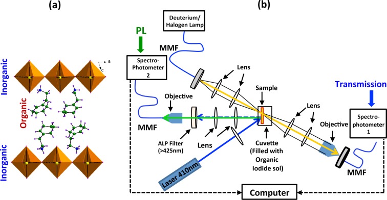
To investigate the dynamics of the intercalation process in real time, simultaneous in situ transmission and photoluminescence (PL) measurements are performed at room temperature (Figure 1b). The deposited PbI2 thin film sample (2.5 × 1 cm size) is inserted into a quartz cuvette, which contains 5 mL of (R-NH3)I solution of the desired concentration. Both transmission and PL are monitored prior to the insertion of the sample and appropriate care is taken to avoid any solvent turbulence during the insertion. The PL is collected in reflection mode using laser excitation (410 nm diode laser, ∼6 mW) with an all long-pass filter (ALP) filter (>425 nm) and focusing by appropriate lenses. For transmission/absorption, a white light broadband source is used. Both the PL and transmission signals are simultaneously collected for more than 300 s at 100 ms intervals, through two separate spectrometers that are synchronized using a computer.
Figure 1.
(a) Schematic of the structure of typical (R-NH3)2MX4 type layered perovskites. (b) Schematic diagram of experimental setup used for simultaneous in situ PL and transmission measurements.
The thickness and surface quality of intercalated and parent films are verified using atomic force microscopy (AFM), surface profilometer and table-top SEM. Glancing angle thin film X-ray diffraction (XRD) studies are carried out with Cu Kα radiation (λ = 1.5406 Å). The white light/PL images (bright field) and spatial PL spectral mappings are performed using a modified confocal microscope, equipped with a computer controlled XY stage, and a MMF (multimode fiber)-coupled 410 nm diode laser. The PL spectra and images are recorded by a spectrometer and high-resolution camera, respectively. Unless otherwise specified, all experiments are conducted at room-temperature and ambient condition.
Results
Typically perovskite powders and single crystals are obtained from conventional chemical processing. During the solution process, the PbI42– anion and R-NH3+ cations are bound together through the hydrogen bonding of N–H···I, which provide a link between the organic and inorganic moieties. Here R can belong to a wide variety of organic functional groups ranging from cyclic to alkyl chain families. Eventually these (R-NH3)2PbI4 unit cells (Figure 1a) self-assemble into sheets of infinitely extended corner-shared PbI6 octahedra separated by organic bications and grow into polycrystallites.14 The size/shape of the organic moieties (mono or bi cations) dictate the effective dimensionality of the corner-shared PbI6 octahedral extended network, forming 0D, 1D, 2D, or 3D perovskites.14 The resultant IO perovskite powders and crystals show many new interesting properties at easily accessible temperatures, compared to their organic/inorganic components.20,21 However, it is a complex task to monitor self-assembly in this solution state.
Recently, we established simple and direct fabrication of high-quality 2D layered perovskites from the intercalation of organic moieties into previously deposited parent PbI2 thin films.24 The rate of intercalation between Pb–I layers critically depends on many factors such as the organic moiety size/shape/functionality, the solvent used, the solute concentration, and the initial parent PbI2 film thickness. All these factors play crucial roles in the nucleation/growth of these layered perovskites and we address such issues below.
The intercalation process has been verified for a wide variety of organic moieties, which have already been established as candidates for 2D perovskite fabrication through conventional chemical methods.24,40 Here, as an example, the intercalation process has been demonstrated for cyclic (C6H9C2H4NH3I) [CHI] and long-chain alkyl-ammonium (C12H25NH3I) [C12I] based organic moieties on deposited PbI2 thin films, so that (C6H9C2H4NH3)2PbI4 [CHPI] and (C12H25NH3)2PbI4 [C12PI] are formed, respectively. For all the measurements shown in Figure 2, the thickness of initial PbI2 film (100 nm) and the concentration of organic iodides (3 mM in benzene) are constant. As mentioned earlier, these IO perovskites are known for strong room-temperature exciton absorption and emission features therefore these parameters are monitored in real time for both cases during intercalation.
Figure 2.
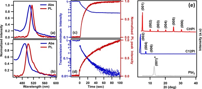
(a, b) Room-temperature exciton absorption and PL spectra and (c, d) real-time intensities of exciton transmission minimum and PL peak during intercalation. Rows a, c and b, d are for (C6H9C2H4NH3)2PbI4 [CHPI] and (C12H25NH3)2PbI4 [C12PI] intercalated films, respectively. (e) Glancing-angle XRD patterns of intercalated CHPI and C12PI perovskite thin films. Parent PbI2 film added for comparison, all XRD patterns shifted along y-axis for clarity (intensities are not be scaled).
After intercalation, CHPI and C12PI films show strong room-temperature exciton absorption and PL features, with peak widths of ∼20 nm (Figure 2a,b).41 The time evolution of exciton transmission and PL are monitored in real time for both samples (Figure 2c, d). In general, the exciton absorption probes the full range of exciton states, whereas the PL only emerges from the lowest available exciton energy levels. As seen in Figures 2c, d, the intercalation rate is slower in the long alkyl C12I compared to the cyclic CHI. However, as discussed below, comparison of intercalation dynamics between such diverse organics is not yet possible to simulate. The presence of strong (00l) peaks in the glancing-angle XRD patterns of the intercalated CHPI and C12PI thin films demonstrate the complete conversion of parent PbI2 to IO perovskite with perfect alternate stacking of inorganic and organic layers (Figure 2e). The effect of organic moiety size on intercalation can also be seen on the d-spacing changes between the Pb–I layers. The C12I (14.705 Å) molecule is much longer compared to CHI (5.037 Å), and a corresponding decrease in the (001) peak angle signifies a d-spacing increase of 17.398 to 23.701 Å from CHPI to C12PI. We note that long alky-ammonium based IO perovskites (C12PI) are well-known for structural phase flips from a stable phase I (orthorhombic) to a metastable phase II (monoclinic).12,42 The data reported here is all for the most stable phase I and the in situ evaluation of these structural phase flips during intercalation will be discussed in the later sections.
3.1. In Situ Intercalation Process Dynamics: Effect of Film Thickness and Solvent
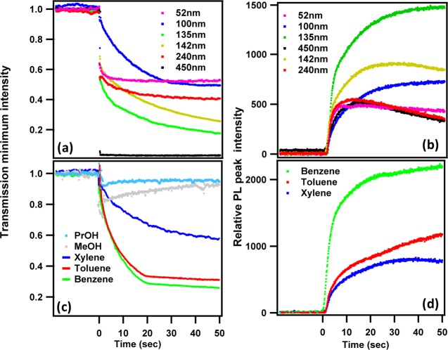
Simultaneous in situ transmission and PL measurements were performed for various thicknesses of PbI2 films ranging from 50 to 450 nm, while keeping the organic moiety (CHI) concentration (3 mM) and solvent (toluene) the same for all cases (Figure 3a, b). The results show that in order to achieve relatively fast and complete intercalation, the optimum PbI2 film thickness is 100–130 nm for this concentration. For thicker (>250 nm) and thinner (<100 nm) films the exciton PL intensities are comparatively low, and after 30 s of intercalation, a decay in the PL is clearly seen. The presence of an optimum thickness suggests that strain may play a role in intercalation as discussed below.
Figure 3.
Real time (a, c) exciton transmission minimum (∼508 nm) and (b, d) PL peak (∼517 nm) intensities during intercalation of organic moiety CHI in PbI2 films. Rows a, b and c, d are for various PbI2 thicknesses (CHI concentration: 3 mM) and for various nonpolar solvents (PbI2 thickness: ∼100 nm), respectively. (Polar solvents propanol (PrOH) and methanol (MeOH) are also shown for comparison.)
The choice of solvent is also crucial to intercalation dynamics. Solvents should dissolve the organic moiety completely, but should not dissolve or modify the surface of PbI2 and/or the resultant IO perovskite films. Here we examined the solvent dependencies for both nonpolar (benzene, toluene and xylene) and polar (alcohols, acetonitrile (ACN) and trichloroethylene (TCE)) solvents. Although all these solvents dissolve the organic well, only nonpolar solvents are appropriate for intercalation as polar solvents showed no signature of exciton formation. Figure 3c, d shows the intercalation dynamics of the exciton transmission minimum and PL peak positions in three nonpolar solvents. For all measurements, the thickness of PbI2 films (∼100 nm) and concentration of CHI (3 mM) were kept constant. While the intercalation process was fastest with benzene, prolonged exposure resulted in damage of the resultant perovskite film surface. Again, we discuss the role of solvent later.
3.2. In Situ Intercalation Process Dynamics: Effect of Organic Moiety Concentration
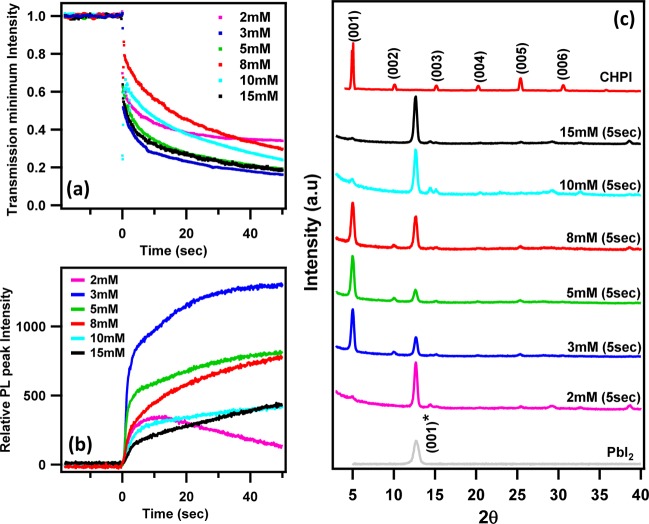
It is important to have an appropriate ratio of inorganic and organic components in the formation of IO perovskites. For stoichiometric synthesis, one needs one unit of MX4–2 cation and two organic bications to obtain one unit of (R-NH3)2PbI4, so the ratio between the organic moiety (R-NH3)I to that of metal halide (MX2) has to be 2:1. Therefore, it is important to provide the required number of organic moieties (i.e., concentration) in order to break the weak van der Waal forces between molecular layers of PbI2 and convert them into extended PbI6 octahedral networks. Figure 4a, b show the transmission and PL dynamics for intercalation of CHI at different solution concentrations. Stable, high PL intensities and a fast rate of intercalation were observed for 3 mM concentrations, but acceptable results were also obtained for 5–8 mM concentrations. For very dilute (<3 mM) and highly concentrated (>10 mM) solutions the resultant films show entirely different PL dynamics, which will be discussed later.
Figure 4.
Time course of (a) exciton transmission minimum and (b) PL peak during intercalation of different concentrations of organic CHI (prepared in toluene) into PbI2 thin films. (c) XRD patterns of PbI2 films intercalated for 5 s in different concentrations of CHI. The XRD patterns of completely intercalated (>20 s) CHPI and parent PbI2 films are also added for comparison (XRD patterns shifted along y-axis for clarity). The PbI2 film thickness is 135 nm for all cases.
To understand the structural phase formation of IO perovskites for various organic moiety concentrations, XRD studies were performed at an intermediate time interval (5 s), as well as on completely intercalated films (Figure 4c, the XRD patterns of unreacted PbI2 films are also added for comparison. Intercalated films with 3–8 mM show strong (001) peaks signifying the formation of highly oriented and self-assembled stacking arrangements with a substantial increase from the parent in layer-to-layer distance, d(001)= 17.63 Å. However, for less-stoichiometric concentrations 2 mM (PbI2 rich) and 10–15 mM (organic rich), XRD patterns are mostly dominated by strong PbI2 peaks, though a weak (001) peak can also be seen. XRD studies thus confirm that optimum concentrations (3–8 mM) of organic moiety are required to obtain the desired IO perovskite. Note that the peak corresponding to unreacted PbI2 phase is still clearly visible at this intermediate stage, because complete conversion requires intercalation for more than 20 s.
As a general observation, for dilute solutions (<3 mM) the PL peak intensity saturates at about 30 s then slowly decreases. One reason for PL degradation could be solvent damage of the resultant IO perovskite. To verify this we performed the experiment in a slightly different way: transmission/PL dynamics are recorded on fully intercalated CHPI films exposed to pure toluene solvent (0 mM). High PL peak intensities were followed by a slow decay, similar to the dynamics observed for dilute concentrations (<3 mM). We note that the control transmission dynamics give an average through the full thickness of a film, whereas PL arises from mostly the topmost layers, therefore the effect of surface damage was not observed in transmission measurements. The results imply that the density of organic moiety is not high enough in <3 mM solutions, so the effect of solvent damage dominates the rest of the intercalation process.
Discussion
While these in situ measurements improve our understanding of the intercalation of RNH2-type organic moieties into MX2-based inorganics, the direction of intercalation, whether perpendicular or parallel to the inorganic sheets, remains unclear. To investigate this, we deposited metal strips (Al, 150 nm thickness, 1 mm wide, ∼900 μm separation) onto 100 nm PbI2 films (on a glass substrate) via thermal vapor deposition (Figure 5a). The structure was exposed to a 5 mM CHI solution (in toluene) for 10s, ensuring that the film was completely immersed in the solution.
Figure 5.
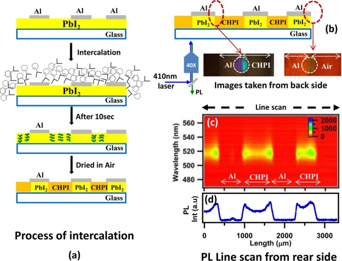
(a) Scheme of intercalation into PbI2 film coated with Al metal strips. (b) PL line mapping performed from the backside of the glass substrate and the corresponding confocal PL images obtained using a 410 nm diode laser. (c, d) Corresponding PL image plot and PL peak intensity across the structures.
PL line scans were performed on a suitably dried structure by illuminating from the transparent substrate side using a 410 nm diode laser focused by a 40X microscope objective, and collecting the PL in reflection mode (Figure 5b). PL images were collected at various locations: the metal capped/uncapped areas and also at the edges of films which were kept open to air. PL line scans taken across complete length of the film show intense green exciton emission (λem ≈ 518 nm) from uncovered areas of the film, while no emission is seen from the metal capped area (insets Figure 5b). PL spectral scans over the complete film length also confirm this (Figure 5c). In the case of metal-capped areas on the edge of the film, emission was observed up to few micrometers from the air interface, and the rest of the capped area remained dark. Note that the Al strips acts as mirror and at the excitation wavelengths, the intensity remains substantial. This implies that initially intercalation starts at the edge-air interface, with organic moieties entering in-between Pb–I layers to form hydrogen bonds with the first available sites. Laterally, the linking of organic with inorganic layers soon creates a complete blockage, preventing further movement of organic moieties along the Pb–I layers. Therefore, the preferential direction of intercalation, from which the organic moieties reach gaps between the PbI2 layers, is preferentially along the c-axis (from the top, perpendicular to the substrate plane).
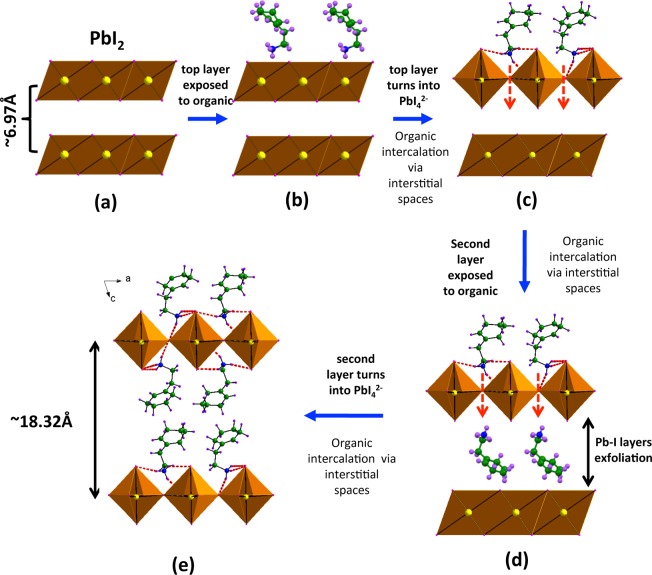
With knowledge of the intercalation process direction, we now suggest a model to explain the layer-by-layer intercalation process. Organic intercalation transforms the extended PbI2 network of edge-sharing PbI6 octahedra (Pb atoms connected by 6 bridging iodine atoms) into the IO hybrid structure of corner-shared PbI6 octahedrons (Pb atoms connected by 4 bridging I atoms, with 2 terminal I atoms). The crystal packing of PbI2 and the inorganic layer of CHPI are shown in Figure 6, as seen along c-axis. The asymmetric unit cell of CHPI crystals contains an open gap between four adjacent PbI6 octahedra with area ∼37 Å2 (Figure 6b), whereas such no gap is available in the case of PbI2 (Figure 6a). The interstices seen in CHPI are typical for IO perovskites, and should be compared to the maximum width of the organic molecules of ∼5 Å. We believe the appearance of these gaps during intercalation allows organic moieties to move through the inorganic layers (and down the c-axis). Our proposed model for layer-by-layer intercalation is shown in Figure 7.
Figure 6.
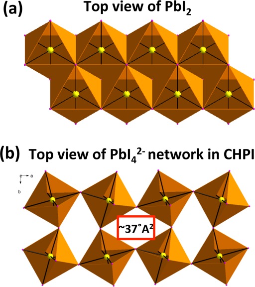
Schematic representation of crystal packing in (a) PbI2 and (b) inorganic layers of CHPI (PbI42– network) seen along the c-axis. (PbI2 space group is P3̅m1 with a = 4.555 Å, b = 4.555 Å, and c = 6.977 Å and CHPI space group is P1̅, a = 12.2053 Å, b = 12.3053 Å, and c = 18.3182 Å).43,44
Figure 7.
Schematic model and speculative digitized sequential intercalation process: (a, b) layered (with interlayer gap of 6.97 Å) parent PbI2, top layer is exposed to organic moiety (R-NH3I); (c, d) modification of top PbI2 layer into extended PbI42– network and intercalation of organic via interstitial spaces and exfoliation of Pb–I layer; and (e) second layer conversion into extended Pb42– network and the resultant (R-NH3)2PbI4 IO hybrid (interlayer separation44 of ∼18.32 Å for CHPI).
When the PbI2 film is exposed to the organic ammonium iodide (C8H13–NH3I) solution, the I atoms on the organic moieties attach to the extended Pb–I network as terminal groups (Figure 7a,b), thereby allowing hydrogen bonding between the −NH3 group and surrounding I atoms (Figure 7c). This interaction leads to the conversion of the PbI2 layer into an incomplete PbI42– network, but also now creates interstices that allow organic molecules to enter the interlayer space and interact with the bottom surface of the layer in the same way (Figure 7d). At this stage, the top inorganic layer is fully converted into an extended corner-sharing octahedral network, where each Pb atom is bonded to two terminals and 4 bridging I atoms. Incoming organic molecules can then similarly convert the second inorganic layer. We note that it was previously shown that the excitons only appears after two PbI42– layers with organic moieties sandwiched in-between are converted.45 Hence this origami-like temporary binding and then reconfiguration of layers happens only when the lower side of each sheet is converted, with strain taken up through this sheet reconfiguration process within the organic interlayer.
We can now discuss our various experimental findings within this model. The wide variety of organic iodide moieties that are found to be effective for intercalation, and their similar dynamics, supports our hypothesis that I-binding to aid the amine-binding is likely. All these molecules have widths that can fit through the openings that are induced in the PbI2 layers. The presence of an optimum initial film thickness seems to be a balance between solvent surface damage for very thin films, and poor adhesion to the substrate for thicker films. We previously also found that induced strain in thicker (>150 nm) IO hybrid films leads to crumpling of the PbI42– layers, and that defect-induced PL then dominates.36 Furthermore, we suggest that the inability of polar solvents to mediate intercalation arises from their ability to reduce the effective internal charge of the organic ammonium iodide, in addition to competitive H-bonding between the polar solvent molecules and the Pb–I network. Both these effects cause charge screening, and inhibit the bond formation required during intercalation.46 It is also note that, in contrast, the polar solvents used here have larger dielectric constants than the nonpolar solvents, which also decreases the effective charge on the organic moieties. The dependence observed on the concentration of organic molecule is then likely arising from the need for cooperative (nonlinear) organic iodide binding to unlock the PbI2 layer rearrangement that gives access to the underside. At high concentrations an opposite effect may arise in which steric hindrance from many molecules binding reduces their passage through the sheet interstices. Thus, we suggest that optimal intercalation is triggered for concentrations just large enough to overcome the van der Waals binding energy between Pb–I monolayers. Although our model then circumstantially accounts for the observations, detailed simulations are required to confirm its exact validity, which is beyond the scope of the current paper.
We now discuss the structural flexibility of these IO materials. An interesting class of longer alkyl-chain-based IO hybrids of type (CnH2n+1NH3)2PbI4 (n = 12, 14, 16, 18), show phase changes of the organic moiety conformation from trans to gauche (and vice versa), causing structural changes in the inorganic network as well. The inorganic sheets are flatter and more strained in phase II structures (I–Pb–I angle = 157.4°), whereas the stable phase I state is more crumpled (I–Pb–I angle = 150.2°). This has potential for creating reversible structural phase transitions at easily accessible device temperatures, with reversible exciton switching already observed.12,42 The optical, electronic, and structural features of these hybrids are critically dependent on structural deformations of the Pb–I bonds in the inorganic layers, as well as the conformation of the organic moiety. So far, thermal-induced exciton flips and phase reversals have been demonstrated only in solution-processed thin films and crystals. However, it has also been shown that such flips are possible due to aging and thickness effects.42 Here, in situ phase changes in these phase-flip IO hybrids are demonstrated at room-temperature. Figure 8 shows the room-temperature exciton PL dynamics obtained for 130 nm thick PbI2 film intercalated with C12I [(C12H25NH3)I]. During the intercalation process the unstable phase II excitons (∼519 nm) arise immediately but saturate in intensity within 20s. However, the most stable phase I exciton (∼501 nm) emerges more slowly and saturates only after 150s. Similar features are observed for n = 14 IO hybrids (not shown here).
Figure 8.

(a) Room-temperature phase I (501 nm) and phase II (519 nm) exciton emission spectra observed during C12I intercalation (5 mM in benzene, 130 nm PbI2 films). (b) Time evolution of PL spectral intensity during C12I intercalation. Inset: PL peak intensity as a function of time for phase I and II excitons.
Conceiving of the phase-flip dynamics at the atomic/molecular level is nontrivial. The fall time of phase II PL matches the rise time of phase I (Figure 8b inset), however the intensity of the phase II exciton does not drop to zero even after the appearance of phase I. This coexistence of both phase I and II excitons suggests a gradual structural rearrangement occurring at the molecular level. In PbI2, Pb atoms are coplanar, so it is easier for intercalation to commence with the flatter phase II inorganic network. As intercalation continues through the film, the phase II exciton signal rises and full intercalation is reached at ∼40 s. Because the top layers in phase II are under less strain compared to lower down at the intercalation front, a phase transition from phase II to the stable phase I can start at the top. Subsequently, this more crumpled inorganic network permeates down through the film at a slower rate.
To further understand the mechanism and kinetics of intercalation, it is essential to establish the nucleation and growth mechanisms of layered perovskites. Recently the nucleation, growth and crystallization of layered materials is often analyzed and explained by simple models such as the Johnson–Mehl–Avrami–Kolmogorov (JMAK) (or simply Avrami) model.28−32 For example, Ma et al. studied polymorphic transformation in titanium disilicide thin film using in situ resistance measurements, XRD, and transmission electron microscopy (TEM), with results accounted for in this model.47 Similarly, the nucleation and growth mechanism of MgH2 thin film multilayers and the hydrogen desorption process were well-explained by JMAK analysis.48
In the present case, the systematic phase transformation of PbI2 (hexagonal) to CHPI (monoclinic), as well as the nucleation and growth mechanisms that occur during the intercalation process can be understood from a simple JMAK analysis.28−32 According to this JMAK growth model, which assumes a steady-state and isotropic transformation from impinging randomly distributed nuclei (here molecules), and with constant growth rate, the time evolution of the transformed volume fraction f(t), at constant temperature is given by
| 1 |
Here the rate constant k represents the nucleation and growth rate, and the Avrami exponent m depends on factors such as growth dimensionality, nucleation mode, saturation of growth, and site selectivity. For unidirectional (1D) growth, m is ∼1, whereas for other dimensionalities and growth saturation, its value is >2.28−32 Assuming multiple dynamical rates are involved in the exciton PL evolution during intercalation (Figures 2-4,8), the above expression can be modified for exciton PL peak intensities (I(t)) as
| 2 |
In Figure 9, some of the example experimental curves (data from Figures 3 and 4) are fitted using eq 2, for both ideal and nonideal intercalation regimes. In the ideal cases, layer-by-layer intercalation of organic moieties into PbI2 proceeds with a single exponential component with m = 0.9–1.1 (region I), strongly supporting the previous argument of unidirectional intercalation along the c-axis (Figures 5–7). The kinetic parameter k–1 is found to be between 10 and 14. However, in nonideal cases, the PL dynamics contains two components, labeled regions I and II. Initially, the intercalation process starts as unidirectional intercalation (region I) with m values ranging between 0.8 and 1.2 and the region spans typically up to 20 s. The latter part of curve is dominated by PL decay (region II), with negative m values ranging from −1.9 to −2.6. The kinetic parameter k–1 of region II is 1 order of magnitude greater compared to region I. For all cases, during the initial few seconds (∼2–5 s, depending on thickness/molarity) the PL intensity follows a pre-exponential component that is likely due to experimental artifacts such as solvent turbulence during intercalation or surface impurities. The JMAK model analysis broadly confirms the typical optimized conditions for a proper (ideal) intercalation: having PbI2 thickness of 100–140 nm and organic iodide concentrations of 3–8 mM in nonpolar solvents (preferably, toluene). Intercalation times are also important (∼20–30 s, depending on thickness, solvent, and concentration). The nonideal region where |m| > 1 with relatively slow kinetic rate suggests that the intercalation process with nonoptimized parameters is dominated by factors such as solvent damage, saturation of intercalation, or emerging poly directional growth. Nevertheless, we are able to account for the intercalation process, which is compatible with the simple model presented above.
Figure 9.

Exciton PL peak intensity variation during the intercalation process of CHI into PbI2 films for various ideal and nonideal cases. (a–c) Ideal cases for optimum organic molarity and PbI2 thickness; (d–f) nonideal cases of intercalation. Plots are labeled with the CHI concentration and PbI2 film thickness. The black lines show theoretical fits using the modified JMAK expression (eq 2, see text).
Conclusion
In conclusion, we greatly improved understanding of the formation of IO hybrid perovskites via the intercalation of organic moieties into parent layered inorganic semiconductors. The evolution of strong room-temperature optical excitons observed in these multiple quantum well systems are systematically monitored during intercalation. For the first time, the dynamics of intercalation has been studied for [(R-NH3)2PbI4] type inorganic–organic perovskites, and it was demonstrated that the insertion of organic molecules into the framework occurs through holes opened progressively into the inorganic monolayers. A basic model is suggested which explains the intercalation dynamics at the molecular level. The successful optimization of various parameters for efficient intercalation has been demonstrated for the organic moiety CHI and PbI2 films, leading to the formation of device quality thin films. Here the best quality films were produced using a 130–140 nm PbI2 films with 3–8 mM CHI/toluene solutions. Unidirectional (1D) growth along the c-axis is confirmed both with patterned samples, and using fits to a simple JMAK nucleation and growth model. Our findings are relevant for the future design and application of metal halide-based 2D IO perovskite thin films and nanostructures.
Acknowledgments
This work is part of High-Impact Research scheme of IIT Delhi, DST-SERC (SR/S2/CMP-0021/2012), Nano Research Facility (MCIT, Govt. Of India), UK-India Education and Research Initiative (UKIERI) programme, and part funded by EPSRC grant EP/G060649/1, and ERC LINASS 320503.
Author Contributions
The manuscript was written through equal contributions of all authors and all authors have given approval to the final version of the manuscript.
The authors declare no competing financial interest.
References
- Khan A. I.; O’Hare D. Intercalation Chemistry of Layered Double Hydroxides: Recent Developments and Applications. J. Mater. Chem. 2002, 12, 3191–3198. [Google Scholar]
- Lee J. Y.; Baljon A. R. C.; Sogah D. Y.; Loring R. F. Molecular Dynamics Study of the Intercalation of Diblock Copolymers into Layered Silicates. J. Chem. Phys. 2000, 20, 9112–9119. [Google Scholar]
- Xu Z.; Zou X.; Zhou X.; Zhao B.; Wang C. W.; Hamakawa Y. Optimum Design and Preparation of a-Si/a-Si/a-SiGe Triple-Junction Solar Cells. J. Appl. Phys. 1994, 75, 588–595. [Google Scholar]
- Hiibner A.; Aberle A. G.; Hezel R. Novel Cost-Effective Bifacial Silicon Solar Cells with 19.4% Front and 18.1% Rear Efficiency. Appl. Phys. Lett. 1996, 70, 1008–1010. [Google Scholar]
- Niemegeers A.; Burgelman M. Effects of the Au/CdTe Back Contact on IV and CV Characteristics of Au/CdTe/CdS/TCO Solar Cells. J. Appl. Phys. 1996, 81, 2881–2886. [Google Scholar]
- Chung B. C.; Virshup G. F.; Klausmeier-Brown M.; Ristow M. L.; Wanlass M. W. 25.2% Efficiency (1-Sun, Air Mass 0) AlGaAs/GaAs/InGaAsP Three-Junction, Two-Terminal Solar Cell. Appl. Phys. Lett. 1992, 60, 1691–1693. [Google Scholar]
- Tang C. W. Two-Layer Organic Photovoltaic Cell. Appl. Phys. Lett. 1986, 48, 183–185. [Google Scholar]
- Ishihara T.; Takahashi J.; Goto T. Optical Properties due to Electronics Transitions in Two-Dimensional Semiconductors (CnH2n+1NH3)2PbI4. Phys. Rev. B 1990, 42, 11099–11107. [DOI] [PubMed] [Google Scholar]
- Stoumpos C.; Malliakas C.; Kanatzidis M. Semiconducting Tin and Lead Iodide Perovskites with Organic Cations: Phase Transitions, High Mobilities, and Near-Infrared Photoluminescent Properties. Inorg. Chem. 2013, 52, 9019–38. [DOI] [PubMed] [Google Scholar]
- Etxebarria J.; Fernandez J.; Arriandiaga M. A.; Tello M. J. Influence of the Thermal Expansion on the Piezoelectric Photoacoustic Detection of Ferro-Paraelastic Phase Transition in (CH3CH2NH3)2 CuCl4. J. Phys. C: Solid State Phys. 1985, 18, L13–L17. [Google Scholar]
- Goto T.; Lthi B.; Geick R.; Strobel K. Elastic Soft Mode in Perovskite-Type Layer-Structure Materials. Phys. Rev. B 1980, 22, 3452–3458. [Google Scholar]
- Pradeesh K.; Baumberg J. J.; Vijaya Prakash G. Exciton switching and Peierls Transitions in Hybrid Inorganic-Organic Self-Assembled Quantum Wells. Appl. Phys. Lett. 2009, 95, 173305–03. [Google Scholar]
- Billing D. G.; Lemmerer A. Synthesis, Characterization and Phase Transitions of the Inorganic–Organic Layered Perovskite-type Hybrids [(CnH2n+1NH3)2PbI4] (n = 12, 14, 16 and 18). New J. Chem. 2008, 32, 1736–1746. [Google Scholar]
- Mitzi D. B. Templating and Structural Engineering in Organic–Inorganic Perovskites. J. Chem. Soc. Dalton 2001, 1–12. [Google Scholar]
- Lee M. M.; Teuscher J.; Miyasaka T.; Murakami T. N.; Snaith H. J. Efficient Hybrid Solar Cells Based on Meso-Superstructured Organometal Halide Perovskites. Science 2012, 338, 643–647. [DOI] [PubMed] [Google Scholar]
- Heo J. H.; Im S. H.; Noh J. H.; Mandal T. N.; Lim C.; Chang J. A.; Lee Y. H.; Kim H.; Sarkar A.; Nazeeruddin M. K.; Grätzel M.; Seok S. I. Efficient Inorganic–Organic Hybrid Heterojunction Solar Cells Containing Perovskite Compound and Polymeric Hole Conductors. Nat. Photonics 2013, 7, 486–491. [Google Scholar]
- Burschka J.; Pelletaaa N.; Moon S.; Humphry-Baker R.; Gao P.; Nazeeruddin M. K.; Grätzel M. Sequential Deposition as a Route to High-Performance Perovskite-Sensitized Solar Cells. Nature 2013, 499, 316–320. [DOI] [PubMed] [Google Scholar]
- Kagan C. R.; Mitzi D. B.; Dimitrakopoulos C. D. Organic-Inorganic Hybrid Materials as Semiconducting Channels in Thin-Film Field-Effect Transistors. Science 1999, 286, 945–947. [DOI] [PubMed] [Google Scholar]
- Era M.; Morimoto S.; Tsutsui T.; Saito S. Organic-Inorganic Heterostructure Electroluminescent Device using a Layered Perovskite Semiconductor (C6H5C2H4NH3)2PbI4. Appl. Phys. Lett. 1994, 65, 676–678. [Google Scholar]
- Muljarov E. A.; Tikhodeev S. G.; Gippius N. A.; Ishihara T. Excitons in Self-Organized Semiconductor/Insulator Superlattices: PbI-based Perovskite Compounds. Phys. Rev. B 1995, 51, 14370–14378. [DOI] [PubMed] [Google Scholar]
- Shimizu M.; Fujisawa J.; Ishi-Hayase J. Influence of Dielectric Confinement on Excitonic Nonlinearity in Inorganic-Organic Layered Semiconductors. Phys. Rev. B 2005, 71, 205306–205309. [Google Scholar]
- Warren R. F.; Liang W. Y. Raman Spectroscopy of New Lead Iodide Intercalation Compounds. J. Phys.: Condens. Matter 1993, 5, 6407–6418. [Google Scholar]
- Coleman C. C.; Magness B.; Melo P.; Goldwhite H.; Tikkanen W.; Tham Q.; Pham K.; Jacubinas R.; Kaner R. B.; Treece R. E. Intercalation of Hydrazines in Lead Iodide. J. Phys. Chem. Solids 1996, 57, 1153–1158. [Google Scholar]
- Pradeesh K.; Baumberg J. J.; Vijaya Prakash G. In situ Intercalation Strategies for Device-Quality Hybrid Inorganic-Organic Self-Assembled Quantum Wells. Appl. Phys. Lett. 2009, 95, 033309–3. [Google Scholar]
- Ogawa M.; Kuroda K. Photofunctions of Intercalation Compounds. Chem. Rev. 1995, 95, 399–438. [Google Scholar]
- Privitera S.; Via F. L.; Spinella C.; Quilici S.; Borghesi A.; Merinardi F.; Grimaldi M. G.; Rimini E. Nucleation and Growth of C54 Grains into C49 TiSi2 Thin Films Monitored by Micro-Raman Imaging. J. Appl. Phys. 2000, 88, 7013–7019. [Google Scholar]
- O’Hare D.; Evans J. S. O.; Fogg A.; O’Brien S. Time-resolved, In situ X-Ray Diffraction Studies of Intercalation in Lamellar Hosts. Polyhedron 2000, 19, 297–305. [Google Scholar]
- Hulbert S. F. Models for Solid-State Reactions in Powdered Compacts. J. Br. Ceram. Soc. 1969, 6, 11–20. [Google Scholar]
- Avrami M. Kinetics of Phase Change. I General Theory. J. Chem. Phys. 1939, 7, 1103–1112. [Google Scholar]
- Avrami M. Kinetics of Phase Change. II Transformation Time Relations for Random Distribution of Nuclei. J. Chem. Phys. 1940, 8, 212–224. [Google Scholar]
- Avrami M. Granulation, Phase Change, and Microstructure Kinetics of Phase Change. III. J. Phys. Chem. 1941, 9, 177–184. [Google Scholar]
- Erofe’ev B. V. Generalized Equation of Chemical Kinetics and its Application in the Reactions Involving Solids. C. R. Acad. Sci. URSS 1946, 52, 511–514. [Google Scholar]
- Granas E.; Andersen M.; Arman M. A.; Gerber T.; Hammer B.; Schnadt J.; Andersen J. N.; Michely T.; Knudsen J. CO Intercalation of Graphene on Ir(111) in the Millibar Regime. J. Phys. Chem. C 2013, 117, 16438–16447. [Google Scholar]
- Liu L.; Yao T.; Tan X.; Liu Q.; Wang Z.; Shen D.; Sun Z.; Wei S.; Xie Y. Room-temperature Intercalation-Deintercalation Strategy Towards VO2(B) Single Layers with Atomic Thickness. Small 2012, 8, 3752–3756. [DOI] [PubMed] [Google Scholar]
- Borja M.; Dutta P. K. Fatty Acids in Layered Metal Hydroxides: Membrane-like Structure and Dynamics. J. Phys. Chem. 1992, 96, 5434–5444. [Google Scholar]
- Pradeesh K.; Baumberg J. J.; Vijaya Prakash G. Strong Exciton-Photon Coupling in Inorganic-Organic Multiple Quantum Wells Embedded low-Q Microcavity. Opt. Express 2009, 17, 22171–22178. [DOI] [PubMed] [Google Scholar]
- Era M.; Hattori T.; Taira T.; Tsutsui T. Self-Organized Growth of PbI-Based Layered Perovskite Quantum Well by Dual-Source Vapor Deposition. Chem. Mater. 1997, 9, 8–10. [Google Scholar]
- Mitzi D. B.; Prikas M. T.; Chondroudis K. Thin Film Deposition of Organic-Inorganic Hybrid Materials Using a Single Source Thermal Ablation Technique. Chem. Mater. 1999, 11, 542–544. [Google Scholar]
- Dwivedi V. K.; Baumberg J.; Vijaya Prakash G. Direct Deposition of Inorganic- Organic Hybrid Semiconductors and their Template-Assisted Microstructures. Mater. Chem. Phys. 2013, 137, 941–946. [Google Scholar]
- Saikumar I.; Ahmad S.; Baumberg J. J.; Vijaya Prakash G. Fabrication of Excitonic Luminescent Inorganic–Organic Hybrid Nano- and Microcrystals. Scr. Mater. 2012, 67, 834–837. [Google Scholar]
- Pradeesh K.; Rao K. N.; Vijaya Prakash G. Synthesis, Structural, Thermal and Optical Studies of Inorganic-Organic Hybrid Semiconductors, R-PbI4. J. Appl. Phys. 2013, 113, 083523–9. [Google Scholar]
- Pradeesh K.; Baumberg J. J.; Vijaya Prakash G. Temperature-Induced Exciton Switching in Long Alkyl Chain based Inorganic-Organic Hybrids. J. Appl. Phys. 2012, 111, 013511–6. [Google Scholar]
- Wyckoff R. W. G. In Crystal Structures; Interscience; John Wiley & Sons, 1963; Vol.1. [Google Scholar]
- Billing D. G.; Lemmerer A. Poly[bis[2-(1-cyclohexenyl)ethylammonium] di-μ-iodo-diodoplumbate(II)]. Acta Cryst. C 2006, 62, m269–m271. [DOI] [PubMed] [Google Scholar]
- Matsui T.; Yamaguchi A.; Takeoka Y.; Rikukawa M.; Sanuia K. Fabrication of Two-Dimensional Layered Perovskite [NH3(CH2)12NH3]PbX4 Thin Films using a Self-Assembly Method. Chem. Commun. 2002, 10, 1094–1095. [DOI] [PubMed] [Google Scholar]
- Kaviyarasu K.; Sajan D.; Selvakumar M. S.; Thomas S. A.; Anand D. P. A Facile Hydrothermal Route to Synthesize Novel PbI2 Nanorods. J. Phys. Chem. Solids 2012, 73, 1396–1400. [Google Scholar]
- Ma Z.; Allen L. H. Kinetic Mechanisms of the C49-to-C54 Polymorphic Transformation in Titanium Disilicide Thin Films: A Microstructure-Scaled Nucleation-Mode Transition. Phys. Rev. B 1994, 49, 13501–13511. [DOI] [PubMed] [Google Scholar]
- Mooij L.; Dam B. Nucleation and Growth Mechanisms of Nano Magnesium Hydride from the Hydrogen Sorption Kinetics. Phys. Chem. Chem. Phys. 2013, 15, 11501–11510. [DOI] [PubMed] [Google Scholar]


