

Abstract
Objective
The edge chipping test was used to measure the fracture resistance of CAD/CAM dental restoration ceramics and resin composites.
Methods
An edge chipping machine was used to evaluate six materials including one feldspathic porcelain, two glass ceramics, a filled resin-composite, a yttria-stabilized zirconia, and a new ceramic-resin composite material. Force versus edge distance data were collected over a broad range of forces and distances. Data were analyzed by several approaches and several chipping resistance parameters were evaluated. The effects of using different indenter types were explored.
Results
The force versus distance trends were usually nonlinear with good fits to a power law equation with exponents usually ranging from 1.2 to 1.9. The order of chipping resistance (from least to greatest) was: feldspathic porcelain and a leucite glass ceramic (which were similar), followed by the lithium disilicate glass ceramic and the two resin composites (which were similar), and finally the zirconia which had the greatest resistance to chipping. Chipping with a Vickers indenter required 28% to 45% more force than with the sharp conical 120° indenter. The two indenters rank materials approximately the same way. The power law exponents were very similar for the two indenters for a particular material, but the exponents varied with material. The Rockwell C indenter gives different power law trends and rankings.
Significance
Despite the variations in the trends and indenters, simple comparisons between materials can be made by chipping with sharp conical 120° or Vickers indenters at 0.50 mm. Broad distance ranges are recommended for trend evaluation.
Introduction
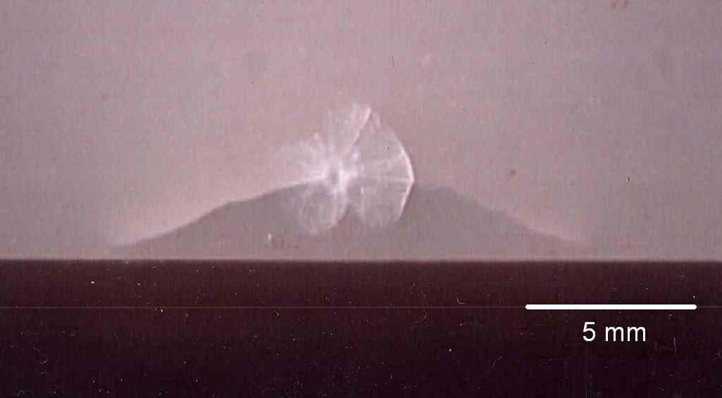
The edge chipping test is used to evaluate the resistance of brittle materials to flaking near an edge as shown in Figure 1. Chips are formed by advancing an indenter into a material near an edge. The force required for chip formation, F, increases with distance from the edge, d. The shape of the chip is usually independent of the material tested.
Figure 1.
This method was originally developed in the late 1980s to study hard metal cutting tools at the National Physical Laboratory in London [1–4]. Later, J. Quinn pioneered the application of this method to dental restorative materials.[5–12] Other groups [13,14,15] are now using it and it has even been used to evaluate human dentin [16] and enamel [17]. A short review paper on edge chipping as applied to dental materials was recently prepared.[12] This method has also been used for many applications other than dental materials [18,19,20,21]. A draft European prestandard was written in 2009 [22].
Chipping is a common failure mode in many dental restorations made of brittle materials. Although the laboratory scale edge chip tests use specific indenters on test blocks with carefully prepared edges, the chips physically resemble some types of in-vivo failures [23,24] and shown in Supplemental Fig 1 in the on-line version of this paper. In addition, edge chipping arising from CAD/CAM machining of dental restoration materials is a major concern [25]. In that study it was shown that the microstructure of the material played a very strong role in determining chip sizes in 90° edges prepared by CAD/CAM milling with a 4 cm grinding disk having 64 µm average grain size diamonds [25].
Unfortunately, divergences in technique, analysis, and reporting of results from laboratory edge chip tests have emerged and the divergences hamper data comparisons. Indenters include the original Rockwell C diamond indenters, Knoop and Vickers pyramidal indenters, and the sharp-tip diamond 120° conical indenter that we favor. The latter is nearly identical to a 120° conical Rockwell C indenter, but the Rockwell C indenter has a rounded tip with a 200 µm radius. In this paper, we will explore some of the differences in testing procedures and the way the results are reported. We will also determine if the edge chipping resistance ranking of materials varies with indenter type.
One criticism of the common lab scale edge chip tests is that they use sharp diamond indenters in very controlled conditions with specimens having nicely-defined 90° edges. People usually do not chew on sharp diamond indenters and teeth do not have flat surfaces with 90° corners. Our objective with the edge chip tests is to conduct chipping resistance experiments under controlled conditions with well-defined indenters and reference configurations. One could apply the same criticism to classic fracture toughness (KIc) tests using compact tension specimens or single-edged precracked bend bars. These configurations are not representative of actual components, but the classical tests do measure a fundamental fracture resistance property under controlled conditions. That is our objective with the edge chip test: measure chipping resistance under controlled conditions.
Edge chipping is a multistep process that entails:
formation of a small indentation
formation of short, stable radial cracks (unless the indenter is blunt, in which case cone cracks form in some materials).
propagation of some of the radial cracks downward and parallel to the side surface.
unstable crack propagation towards the side surface causing a flake to pop off.
Early work [1–4,19,20] emphasized the relationship between edge toughness and traditional fracture parameters such as KIc, the fracture toughness; GIc, the critical strain energy release rate; or γf, the fracture surface energy. Most investigators graph the edge chip data as force versus distance and use linear repression to fit the data. The slope is interpreted as the “edge toughness, M, or Te.” It has units of force/distance which is dimensionally analogous to (force·distance)/area or energy/area. Thus, it should not be surprising that the edge toughness sometimes correlates better with GIc or γf than with KIc.
The objectives of this paper are to show typical edge chip results for six commercial CAD/CAM restoration materials, compare results from different indenters, and report outcomes using alternative resistance indices. It is hoped that this work will contribute to refinements to the CEN draft standard for technical ceramics [22] so that it will be useful to the dental community. The new data in this paper may also be useful for modeling of the edge chip process. Results are analyzed with the two force versus distance functions (linear and power law) that have been customarily applied to edge chipping data. Part 2 [26] includes a more comprehensive analysis of the results including correlations with traditional fracture toughness parameters and presentation of a new force-distance function based on a phenomenological model that overcomes some of the limitations of the power law fit used in this paper.
Two hypotheses are set forth in this paper: indenter type does not affect test results, and force versus distance data follow a linear trend.
Materials
The six commercial materials that were tested are listed in Table 1.a Test specimens for the various materials varied in size and shape from 3 mm by 4 mm cross section sized bend bar fragments to larger square blocks of 10 mm to 20 mm length per side. The two feldspathic porcelains, one glass ceramic, and a new ceramic-filled composite were available in the form of four to five wear test type rectangular blocks cut from CAD/CAM blanks. Spare bend bars or broken bend bar fragments, typically 3 mm × 4 mm × 15 mm to 20 mm were used for a yttria-stabilized zirconia and the filled resin composite. Care was taken to grind and the surfaces to make well-defined, reproducible edges. Specimen preparation procedures varied with the materials, but the final step was polishing with 4000 grit SiC paper while wet. For the bend bar specimens, coarse-grit initial grinding was used to remove the ~ 0.15 mm sized chamfers that were on the long edges.
Table 1.
Material properties#
| Material | H* (GPa) |
E** (GPa) |
ρ (g/cm3 |
KIc*** (MN/m1.5) |
GIc† (J/m2) |
B†† (µm−1) |
Ref. | |
|---|---|---|---|---|---|---|---|---|
| zirconia, 3Y-TZP (3M-ESPE Lava) | HV, 12.3 | 210 | 6.1 | (~10) | - | 27 | ||
| HK2, 11.2 (0.2) | 216 res | - | 4.8 (0.6) | fract | 109.7 | 122.0 | unpubl. | |
| lithium disilicate glass ceramic (Ivoclar, IPS e.max CAD) | HV, 5.7 (0.2) | 95 (5) | 2.5 (0.1) | 2.0 – 2.5 | SEVNB | 42 – 66 | 87 – 135 | 34 |
| nanoceramic filled composite (3M-ESPE Lava Ultimate) | HV1, 1.05 (0.01) | 14.8 | 1.94 | 2.02 (0.15) | SEVNB | 276 | 3.8 (0.1) | 28 |
| filled resin composite (3M-ESPE Paradigm, MZ100) | HK, 0.99 (0.02) | 12.2 defl | 2.13 | 1.1 (0.2) | fract. | 99 | 9.98 | 11 |
| - | 12 defl | - | 1.3 (0.1) | SBCN | 35 | |||
| - | - | - | 1.21 (0.07) | CT††† | 37 | |||
| HV1, 1.31 (0.02) | - | - | 1.64 (0.15) | SEVNB | 28 | |||
| feldspathic porcelain (Vita Mark 2) | HV, 6.3 (0.3) | 69.7 res | 2.4 | 1.19 (0.05) | SEPB | 20.3 (1.7) | 311 (41) | 5 |
| HV1, 6.1 (0.4) | - | - | 1.45 (0.09) | SEVNB | 28 | |||
| leucite glass ceramic (Ivoclar IPS Empress CAD) | HV1, 5.6 (0.2) | 66.8 res | 2.4 | 1.03 (0.03) | SEVNB | 15.9 (0.9) | 352 (33) | 5 |
| HV, 5.8 | - | 1.2 | SEVNB | 32 | ||||
| HV, 6.2 | 62 | - | 1.3 (0.1) | SENB | 32,33 | |||
| HV1, 5.3 (0.4) | - | - | 1.44 (0.1) | SEVNB | 28 | |||
Uncertainties are one standard deviation and are listed with the number of significant figures from the original source if available.
Load-independent hardness at a load large enough that hardness had reached a plateau; HV = Vickers, HK = Knoop
Elastic modulus methods: res = beam resonance at natural frequency, impulse excitation; defl = 4-point beam deflection
Methods: SENB = single edged notched beam; SEPB = single edged precracked beam; SEVNB = single edged V-notched beam; CT = compact tension; fract = fractographic analysis of well-defined flaws in bend bars; SBCN = short bar chevron notch
Critical strain energy release rate, GIc = KIc2/E
Brittleness, computed from B = HE/KIc2
Plateau value for the rising R-curve (0.9 to 1.2 MN/m1.5) by the CT method. The material in Ref. 36 was a slightly different version than the one in this study.
The 3 mol % yttria stabilized zirconia (Lava™ 3Y-TZP, 3M-ESPE, St. Paul, MN, USA) had a grain size of 0.5 µm [27]. The material is typically fabricated in the form of milling blanks for CAD/CAM machining. Large fragments of bend bars (3 mm × 4 mm × 45 mm) from an earlier study were used for the edge chipping experiments. Top and side surfaces were progressively hand ground wet with a rotary polishing wheel using 600, 800, 1000, 1200, 2400, and 4000 grit wet SiC papers. The three coarse-grit papers were necessary to remove the chamfers on the long edges of these bend bar fragments.
A new resin nano-ceramic filled composite (Lava-Ultimate,™ 3M-ESPE, St Paul, MN, USA) is described by the manufacturer as being composed of a resin filled with as much as 0.80 mass fraction silica (20 nm) and zirconia (4nm to 11 nm) ceramic nanoparticles and clusters. Recent results suggest that the combination of fracture toughness, hardness, and elastic modulus of this material is very favorable and it has a low brittleness index [28,29,30]. Brittleness, defined as B = HE/KIc2, is the ratio of a material’s plastic deformation resistance to fracture resistance and relates to behavior around indentations [29,30]. The average nanocluster size is 0.6 µm to 10 µm. The material was available in the form of 5 mm × 13 mm × 22 mm blocks. Wet SiC papers, starting with 1200 grit and then progressing to 2400 and 4000 grits, were used to polish all surfaces.
A feldspathic porcelain (Mark II,® Vita Zahnfabrik, Bad Sackingen, Germany) was also tested for comparison to the newer ceramic materials. Experiments were done using blocks that were 9 mm × 10 mm × 15 mm in size. Wet SiC papers starting with 1200 and then progressing to 2400 and 4000 grits were used to polish all surfaces. We also tested 3 mm × 4 mm × 28 mm bend bars left over from earlier studies [5,31]. A detailed characterization of this material including its microstructure, fracture origins, and fracture toughness has been described in Ref. [30]. Limited edge results for this material on bend bar fragments were also available from the work of J. Quinn [5]. This fine-grained porcelain chips relatively easily and we use it as a quasi-reference material in our edge chipping work.
Two glass ceramics were evaluated. One was a leucite glass ceramic (IPS Empress® CAD, Ivoclar-Vivadent, Schaan, Liechtenstein) available in the form of 9 mm × 11 mm × 15 mm blocks [32,33]. The other was a lithium disilicate glass ceramic (IPS e.max® CAD, Ivoclar-Vivadent, Schaan, Liechtenstein) [34] that was available in the form of 8 mm × 11 mm × 15 mm blocks. Wet SiC papers with 1200, 2400, and 4000 grits were used to polish all surfaces.
The commercial filled resin-composite (Paradigm™ MZ100, 3M-ESPE, St. Paul, MN, USA) was described in company literature as containing 0.85 mass fraction spherical sol-gel derived particles comprising nanocrystalline zirconia in silica [35]. The spherical particles averaged 0.6 micrometers in size, but had a broad size distribution. They are in a highly cross-linked polymeric matrix of bis-GMA and TEGDMA. Bend bars of size 3 mm × 4 mm × 18 mm, left over from an earlier study [11] were used for the edge chipping Additional details on this material, including early edge chip results by J. Quinn, as well as hardness, flexural strength, fracture toughness measurements, and comprehensive fractography of the strength-limiting flaws are in Ref. [11]. Wet SiC carbide papers from 1200 to 4000 grit were sufficient to grind the bend bars and to remove the chamfers.
Methods
A commercial edge chipping machine (Engineering Systems Model CK 10, Nottingham, UK) (and shown in Supplemental Fig 2 in the on-line version of this paper) was used to make the chips. The 1000 N load cell readout resolution was 0.1 N and the load cell was certified to be accurate to better than 0.1 N. A reference mass with a certificate traceable to NIST standards was used to verify the accuracy of the load cell. The apparatus had a moveable head with the diamond indenter and a locating microscope. This is like many common indentation hardness type machines. Hence, we could set the edge distance to a prescribed value prior to a test.
It is essential to rigidly mount the test piece; otherwise it might tilt during loading or get nudged sideways by the indenter when a chip pops off. Double-sided sticky tape was tried but was unsatisfactory since it was too compliant. All test pieces are now rigidly waxed onto a mounting plate. At the beginning of a test sequence, the indenter was positioned over a flat portion of the specimen well away from the edges, and a small indentation was made. The instrument crosshair was then precisely lined up with the center of the indentation. The X-Y stage (which had a resolution and accuracy of 0.01 mm that was verified by a NIST calibrated stage micrometer) was used to make indentations at prescribed distances from the edge. The stage was locked in position at the start of a chip test to eliminate any lateral shift. We initially placed chips far away from each other, but gradually we spaced them closer in order to get more chips and data points per specimen. Care was taken to avoid chip overlap. Force was gradually applied in displacement control at 1 mm/min or 3 mm/min until fracture. The forces increased linearly during the loading sequence with the exception that a slight hesitation of a few seconds occurred at about 35 N – 45 N as the mass of the machine head (about 3 kg) shifted on the drive screws. For the six materials in this study, the chips popped off suddenly with an audible snap. The polished side surface of specimens as visually observed with a hand magnifier during the chipping sequence and no side bulging was detected. Very rarely, and only on the relatively compliant composite materials, did a chip pop through the specimen with an audible snap, but did not entirely detach. The faster speeds were used on some of the composite materials. The chipping sequence took 5 s to 30 s depending upon the material and edge distance. Relative humidities were measured with a sling psychrometer and ranged from 35% to 55%. Temperatures were 20° C to 25° C. When a chip popped off, a sudden force drop off was detected by the break-load detection circuitry of the machine. The indenter was extracted automatically and the peak load recorded.
One problem detected in some of our early work, was “overchipping.” Ideally, once a chip pops off, the indenter should instantly extract. In reality, indenter extraction was not instantaneous. The indenter momentarily continued to contact the intact side of the test piece and could make additional damage and a larger indentation. We verified this by interrupting some chips just prior to their popping off and comparing the indentation size and chip sizes to those where the chip was allowed to pop off. This overchipping behavior severely affected measurements of the edge distances by posttest examination and distances sometimes were overestimated. The matter was worse in compliant materials. When a full chip formed, it might not pop completely off and would only partially detach. In this study, edge distances were precisely set prior to each test in order to avoid interpretation problems of the contact site for measurement of the edge distance.
Another matter is the number of chips, N, that should be made. Some of J. Quinn’s early (1998 – 2000) force - distance curves [5] were based on as few as ten chips, but more chips are better for statistical reasons. Uncertainties in the edge toughness, Te, estimates, which are based on the slope of the line through the force-distance data, are reduced if more data are collected. Twenty to thirty-five chips are now typically made.
We primarily used 120° sharp conical, single crystal diamonds. The indenters were fashioned from simple, inexpensive ($25 in 2012) hand scribers used to mark the surface of hard materials (model HS301-120, Gilmore Diamond Tools, Attleboro, MA, USA). The aluminum scriber handles were cut off and the diamond scribe end inserted into the edge chipping machine as shown in Figure 3b. Tip radii are 5 µm or less and the included angles are within 1° of 120°. They were inspected frequently for tip damage and replaced when necessary. These indenters are durable and expendable. They have the advantage that the indenter footprint geometry is self-similar, irrespective of the force applied or the depth of indentation. This is unlike the rounded-tip Rockwell C indenter, whereby at low loads only the relatively blunt tip is engaged. The contact geometry changes to include the rounded sides and even the conical sides as loads increase for greater edge distances. A number of experiments were done in this study with Rockwell C indenters and Vickers indenters for comparison.
Figure 3.

There are two approaches to collecting edge chip data. Sometimes data are collected over a broad range of distances and forces. Alternatively, data are collected at a single arbitrary distance, say 0.5 mm. Practical concerns also may dictate how much data are collected. Much of the early work by J. Quinn [5] was done with 0.1 mm to 0.3 mm distances from an edge, since she used small bend pieces and there was not enough material to make large chips. Larger chips at distances of ≈ 0.5 mm would have been impractical since only a few could be obtained on a bend bar and the chips would have broken through the bottom of the test piece rendering the test invalid. In the present study, more material and thicker pieces were available and chip data was collected for distances up 0.60 mm. Although distances as small as 0.05 mm could be tested, we found it more practical to start at 0.10 mm. Other similarities and differences between the present and earlier work are discussed in Ref. [12].
All distances were from the specimen edge to the center of the point of load application. Most researchers use this convention. Analytical fracture mechanics models that are relevant to the edge chipping problem usually are based on the axis of load application. In contrast, one group [20,21] has advocated measuring distance from the edge to the furthest damage at the indentation site. The size of an indentation damage scar depends upon the extent of indenter penetration and may change drastically with depth of penetration with a rounded tip Rockwell C indenter. Overchipping, described above, may also invalidate posttest chip distance measurements.
Different indices of edge chip fracture resistance may be obtained as listed in Table 2. For many glasses and ceramics, the force – distance trend is linear:
| (1) |
where F is the chipping force and d is the distance from the edge. The slope of the fitted line (usually in terms of force in Newtons per millimeter distance) describes the susceptibility of the material to edge chipping and has been defined as the edge toughness, M or Te, (N/mm). Te is numerically equivalent to the force necessary to create a chip at a distance of 1 mm.
Table 2.
Edge chipping fracture resistance parameters
| Parameter (units) | Meaning | Reference |
|---|---|---|
| edge toughness, Te, or M (N/mm) | Slope of the Force versus distance curve, (or the force to make a chip at 1 mm) | McCormick, Almond 2,3 J. Quinn, 6,7,8 |
| edge chip resistance, ReA (N/mm) | Average Force/distance ratio for many chips | CEN prestandard 22 |
| edge chip power law constant, A, (N/mmn) | Constant in the power law eq. 2 (numerically the force to make a chip at 1 mm) | J. Quinn, 7,10 |
| edge strength, SE (0.5) (N) | Force to make a chip at a distance of 0.5 mm | Watts, Silikas et al, 13, 14 |
There are many cases (e.g., refs. 4,6,9,10) where a much better fit is obtained with a power law:
| (2) |
where n is a constant, usually from 1 to 2. A is a constant with units of N/mmn, and is numerically equivalent to the force to create a chip 1 mm away from an edge. If n = 1, A is identical to Te. The right side of eq. 2 shows an alternative form, whereby A´, the edge chip power law constant, has units of N, and do is an arbitrary distance in mm.b For reasons explained below, a do of 0.5 mm has been chosen in this work.
The significance of the different data analysis trends (linear versus power law), and the problems they pose for reporting of results, are discussed below. Edge chip resistance may be correlated to fracture toughness for many materials, but a discussion is deferred to Part 2 [26].
Watts et al. [13,14] have defined an edge strength, SE (0.5) with units of N, which denotes the force necessary to create a chip at an arbitrary distance of 0.5 mm, which is felt to be a clinically relevant distance.c From eq. 1, it is readily apparent that the numerical value of the edge strength, SE (0.5) with units of N is exactly one half the numerical value of the edge toughness, Te, which has units of N/mm.
The draft CEN standard [22] specifies that edge chip resistance, ReA be reported as the ratio of force, F, divided by distance, d, and has units of N/mm. This ratio is computed for each and every chip. The overall edge chip resistance, , is the average value of the individual results:
| (3) |
The edge chip resistance is very similar to, but not exactly the same as the edge toughness. Both have units of N/mm. Te is the slope of a regressed line through many data points collected over many distances. is the average of all the individual F/d ratios. If the data are linear and are tightly clustered about the line, then edge toughness, Te, and edge chip resistance, , are the same. The CEN draft standard recommends that edge chips be made at a starting distance of 0.5 mm, but then other distances may be used as required depending upon the material. Although this distance is the same as advocated by Watts et al., [13,14] the interpretations of the data are different. The edge chip resistance, , is a force to distance ratio. The edge strength, SE (0.5) is a force.
In this study, we have used a range of distances in order to evaluate the chipping resistance and the various parameters over a broad range of conditions. Differences between parameters are best appreciated from the first results example shown next.
Results
The results are presented in a series of figures, one for each material, plus a master Table 3 that shows all the edge chip resistance parameters. The goals were to: find the best fits to the data, compare the chip resistance parameters, study the effects of indenter type, and compare materials. To avoid overwhelming the reader with too many numbers, the results are presented in an orderly, systematic manner that leads to clear conclusions. We start with a simple example.
Table 3.
Edge chip results†
| Material | IndenterX | Distance range, d (mm) |
NXX | Edge Toughness Te, slope of linear eq.1 (N/mm) |
Edge Chip Resistance, ReA avg. all chips eq. 3, (N/mm) |
Power law eq. 2 |
Edge strength SE (0.5) (N) calculated* |
Edge strength SE (0.5) (N) measured** |
Ref. |
|---|---|---|---|---|---|---|---|---|---|
| zirconia, 3Y-TZP (3M-ESPE Lava) | 120° SC | 0 – 0.50 | 35 | 601 (21) | 536 (100) | F = 715 d1.18 (0.03) | 301 | 301 (21) | new |
| Vickers | 0 – 0.50 | 27 | 743 (37) | 649 (138) | F = 1162 d1.45 (0.02)★ | 426 | 418 (7) | new | |
| lithium disilicate glass ceramic (Ivoclar, IPS e.max CAD) | 120° SC | 0 – 0.60 | 33 | 243 (20) | 193 (71) | F = 437 d1.71 (0.05)★ | 134 | 138 (19) | new |
| nanoceramic filled composite (3M-ESPE Lava Ultimate) | 120° SC | 0 – 0.60 | 35 | 255 (18) | 202 (72) | F = 403 d1.61 (0.04)★ | 132 | 146 (17) | new |
| Rockwell C | 0 – 0.60 | 31 | 287 (11) | 262 (39) | F = 354 d1.25 (0.03) | 149 | 148 (5) | new | |
| Vickers | 0 – 0.60 | 36 | 342 (20) | 277 (90) | F = 574 d1.65 (0.08)★ | 183 | 183 (13) | new | |
| filled resin composite (3M-ESPE Paradigm, MZ100) | 120° SC | 0 – 0.28 | 15 | 120 (13) | 107 (28) | F = 366 d1.72 (0.11)★ | 111 | - | 11 |
| 172 NZ | - | 11 | |||||||
| filled resin composite (3M-ESPE Paradigm, MZ100) | 120° SC | 0 – 0.60 | 84 | 213 (12) | 158 (70) | F = 419 d1.83 (0.03)★ | 118 | 119 (23) | new |
| Vickers | 0 – 0.50 | 31 | 229 (17) | 198 (59) | F = 522 d1.79 (0.07)★ | 151 | 131 (16) | new | |
| feldspathic porcelain bend bars (Vita Mark 2) | 120° SC | 0 – 0.50 | 26 | 138 (5) | 129 (19) | F = 168 d1.20 (0.04)★ | 73 | 69 (5) | new |
| feldspathic porcelain bend bars (Vita Mark 2) | 120° SC | 0 – 0.40 | 32 | 119 (9) | 104 (25) | F = 226 d1.50 (0.06)★ | 80 | - | new |
| feldspathic porcelain blocks (Vita Mark 2) | 120° SC | 0 – 0.60 | 35 | 164 (10) | 142 (37) | F = 238 d1.46 (0.05)★ | 87 | 91 (9) | new |
| Rockwell C | 0 – 0.60 | 27 | 327 (25) | 365 (52) | F = 284 d0.80 (0.03)★ | 163 | 145 | new | |
| Vickers | 0 – 0.60 | 31 | 224 (12) | 184 (54) | F = 370 d1.55 (0.03)★ | 126 | 125 (10) | new | |
| leucite glass ceramic (Ivoclar IPS Empress CAD) | 120° SC | 0 – 0.60 | 34 | 158 (11) | 132 (40) | F = 246 d1.52 (0.06)★ | 86 | 78 (6) | new |
| 120° SC | 0 – 0.32 | 14 | 94.6 (7) | 88 (11) | F = 106 d1.10 (0.06) | 49 | - | 5 | |
| 108 (6) NZ | 5 | ||||||||
Uncertainties, if available, are one standard deviation
SC denotes sharp conical
N is the number of chips
Best fit of either the linear function (eq. 1) or the power law (eq. 2) based on the correlation coefficient, R2. If the R2 values are similar (within 0.04), then no star is shown.
Evaluated from the calculated value for d = 0.5 mm based on the best fitted function. If the linear and power law calculated fits are similar, this entry is the average of the two calculated SE (0.5) values.
Evaluated from the actual data collected at d = 0.5 mm
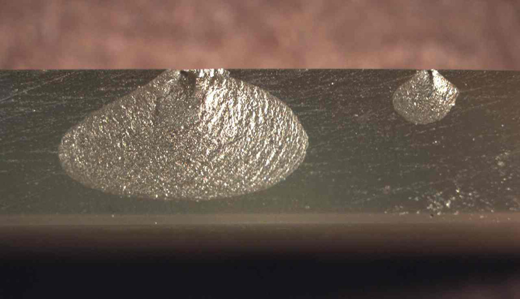
Figure 2, with results for the leucite glass ceramic, shows a linear fit with zero intercept and a simple power law function. The insert shows a typical chip. (Additional illustrations of many chips fork this work are in the online version of this paper.) Earlier results by J. Quinn in Ref. [5] over a more limited distance range are also shown. Her set was generated with bend bar fragments using a more primitive edge chipping machine as discussed in Ref. [12]. (Load was applied by a lever beam and overchipping may have been a problem.) The two data sets are initially in good agreement, but diverge at larger distances. The power law fit to the new data with an exponent of 1.52 seems to be a better fit by a simple visual examination of the data. This is borne out by the correlation coefficient, R2, of 0.951, which is much better than the 0.865 for the linear fit. The seventh row of Table 3 shows both the linear and power law fit parameters for the leucite glass ceramic. The edge chip resistance parameters for the leucite glass ceramicin Table 3 are now considered in turn. The edge toughness, Te, from the slope of the linear regression line through zero, is 158 N/mm, with a standard deviation of 11 N/mm. The standard deviation of the edge toughness, Te, was calculated from:[36]
| (4) |
where N is the number of chips and R2 is the correlation coefficient for the regression fit with zero intercept using an Excel spreadsheet regression analysis. The regression fit parameters for the power law function (eq. 2) were computed by Excel and were corroborated by the Grapherd software package. The standard deviation of the power law exponent n was computed from the regression of the transformed variables (log F and log d). It was small for most of the materials in this study and typically only 0.03 to 0.05. 95% uncertainties for the exponent values are about double the standard deviation, on the reasonable assumption that uncertainties are normally distributed.
Figure 2.

The edge strength, SE (0.5) for the leucite glass ceramic can be judged by the vertical dashed line in Figure 3. It can be estimated three ways. The average of the three chips actually made at that distance, SE (0.5), is 78 N (6 N). (The uncertainty in brackets is one standard deviation.) The d = 0.5 mm intercepts with the linear and the power law fits give: SE (0.5) = 79 N and 86 N, respectively. Table 3 shows the latter computed value, since the power law fit was the better of the two and is starred in the table. The edge chip resistance, , the average value of the thirty-four F/d ratios computed in accordance with the CEN prestandard, was 132 N/mm (40N/mm), a value comparable to, but not identical to the edge toughness, Te = 158 N/mm. Individual edge chip resistance values for the chips ranged from 47 N/mm to 243 N/mm, accounting for the very large standard deviation (40 N/mm) and coefficient of variation of 30%. The average F/d chip ratio, , approach has one serious drawback when applied to data collected over a broad distance range. Equation 3 shows that each chip outcome is weighted the same as any other. The ratio for a small chip made at d = 0.10 mm is weighted the same as the ratio for a chip made at d = 0.40 mm or 0.50 mm. It does not seem reasonable to weight the small chips so much, since the uncertainties in the measured quantities of force and distance expressed as percentages are greater and the edge chipping tests are susceptible to start up processes. If the data are nonlinear, as in the present study, then an average F/d ratio is problematic.
Results for the lithium disilicate glass ceramic with the 120° sharp conical indenter are shown in Figure 3. The power law function is a much better fit for this material and it has a much more pronounced exponent (1.71) than that for the leucite glass ceramic (1.52). Comparing Figures 2 and 3 and the entries in Table 3, all measures of chip resistance indicate the lithium disilicate glass ceramic is more chip resistant than the leucite glass ceramic.
Figures 4a and 4b show new 120° sharp conical, Vickers and Rockwell C outcomes for the feldspathic porcelain. The same material was previously evaluated by J. Quinn in 1998 [5,6], but using a rudimentary self-made chipping machine described in Refs. [5,6,12]. The force-distance trends vary dramatically with indenter type. Figure 4b shows the Rockwell C indenter requires more force to create a chip than either the Vickers or the 120° sharp conical indenters. Over short distances (e.g., 0 mm to 0.30 mm), the data might seem to be best fit by a linear trend, but the power law fit emerges as a better fit as the range extends to 0.60 mm. Figure 4a and Table 3 show three estimates for the sharp conical 120° edge toughness, Te, for this material, which we have evaluated several times over the years. This allow an estimate of the repeatability of the method. The estimates, from highest to lowest, are: 164 N/mm from tests on thick blocks, and 138 N/mm and 119 N/mm from tests on smaller bend bar pieces. Some of the variability is due to the different distance ranges over which the data was collected. There were two batches of material as well. The broader the distance range (e.g., 0 mm – 0.6 mm), the greater is the linear regression slope. This underscores the limitations of using a linear best fit if the data are in fact nonlinear. Figure 4b shows the Rockwell C and Vickers results compared to the best sharp conical 120° data of Figure 4a. Using the values of the calculated edge strengths, SE (0.5), the Vickers indenter required 45% more force (126 N / 87 N) to make a chip than the sharp conical indenter. The effect of indenter type on results is considered further in the discussion section of this paper and in Part 2 [26].
Figure 4.


Outcomes for the filled resin composite are shown in Figure 5. The power law was superior for both the sharp conical and Vickers indenters. One older data subset of 15 sharp conical chips over a short distance range up to 0.28 mm by J. Quinn, Ref. [11] is also shown because this subset fits very well with the entire data set of 84 chips. The subset data appeared to be fit by a linear relationship, but it is clear that when data is collected over a broader range the power law fit is superior. The ratio of calculated edge strengths, SE (0.5), showed that the Vickers indenter required 28% more force to make a chip than did the sharp conical indenter. The indentation sizes were quite large in this softer material, in part due to a momentary pulse of the indenter when the chip popped off.
Figure 5.

The results for the new nanoceramic filled composite are shown in Figure 6. The power law again was the better fit for all three indenters and the sharp 120° conical indenter required the least force to form chips. The ratio of the calculated edge strengths, SE (0.5), showed that the Vickers indenter required 39% more force to make a chip than the sharp conical indenter. For this softer material, the Vickers indenter required more force than did the Rockwell C indenter for distances greater than 0.4 mm. The power law function was the best fit for all three indenters.
Figure 6.

Figure 7 shows the results for 3Y-TZP zirconia, the most chip resistant material. This was the only material where a linear function fit the data, but only with the sharp conical 120° indenter. The power law was superior for the Vickers data. The ratio of the calculated edge strengths, SE (0.5), showed that the Vickers indenter required 42% more force to make a chip than did the sharp conical indenter.
Figure 7.

Discussion
Data range
One outcome is that one must collect data over a sufficient interval if the goal is to discern the proper data trend (linear or power law). Trends that appeared linear at short distance intervals (0 mm to 0.30 mm) were revealed to be nonlinear once data was collected over a broader range. Only for the zirconia did an apparent linear trend over short distances remain linear over broader range (Figure 7) and only for the sharp conical 120° indenter. It may be concluded that if the objective is to compare the chip resistance at a set distance, e.g., 0.50 mm, then it is prudent to collect data at this distance and not extrapolate data collected at shorter distances. In practical terms, this means that specimens should be at least 5 mm thick. Cracks and chips are likely to penetrate all the way through to the bottom of a test piece if thinner specimens are used, probably invalidating the outcome. Furthermore, chips made at larger distances, 0.50 mm and 0.60 mm, are very large and sometimes only a few of these can be obtained on small pieces such as bend bars. For these reasons, it is recommended that wear test type specimens, e.g., rectangular blocks of approximate size (10 mm to 15 mm) by (15 mm to 20 mm) by (5 mm to 10 mm thick), be used for edge chipping experiments. Such larger pieces are easier to grind and polish square, without rounded edges, than bend bars and one can obtain 15 to 20 chips per block. Two such wear blocks per material are used for our routine work.
Material comparisons
Figure 8a compares the data for all materials with the 120° sharp conical indenter. The 3Y-TZP zirconia has the greatest edge chip resistance. The new nano-ceramic composite, the lithium disilicate glass ceramic, and one filled resin composite were next, and they have very similar resistances. The least resistance was for the feldspathic porcelain and the leucite glass ceramic that have almost identical behavior. The sharp conical 120° indenter data trends do not cross over. So a material with a superior chip resistance at 0.3 mm is also superior at 0.50 mm. This allowed easy ranking of materials. Hence, a single edge chip resistance force at an arbitrary distance, say 0.50 mm as advocated by Watts et al. [13,14] and implied in the CEN prestandard [22], is eminently suitable for routine evaluations and comparative purposes. Figure 8b shows the same curves for the four materials that were evaluated with the Vickers indenter. The rankings remain about the same.
Figure 8.


Effect of Indenter type
Indenter type had a pronounced effect on the quantitative outcomes. One cannot interchange the edge chip resistances, either as the slope of the line, or as a force at a set distance (0.5 mm), or even the type of data trend (linear or power) between sharp conical, Vickers, and Rockwell C indenters. In our experience with these and other materials [12], the usual outcomeis that the 120° sharp conical indenter requires the least force and has the lower slopes, followed by the Vickers indenter, and the Rockwell C indenter. Although the Rockwell C indenter and the sharp conical indenters have 120° included angles, the rounded tip of the former makes it a blunt indenter at low forces and short distances. Part 2 [26] shows that the difference can largely be accounted for by the sharpness (the included angle) of the indenter. The 120° sharp conical indenter is sharper than the Vickers indenter and they are both sharper than the relatively blunt Rockwell C indenter. The key factor is the sideways wedging forces that each indenter creates as it penetrates the surface.
Since edge chip resistance varies with indenter type, intercomparsion of data from different studies is difficult [12]. Morrell and Gant [4] and Gogotsi and Mudrik [20,21] have commented on the different responses to different indenters. One important reason for the differences stems from the multistep process discussed in the introduction. Different indenters alter the initiation and propagation steps, and alter the ratio of energy expended in fracture versus deformation processes. Furthermore, the initial extension of short cracks into the bulk and the propagation down parallel to the edge (step c) may be sensitive to loading rate and environment. These may stem from slow crack growth effects in glasses and ceramics, relaxations in polymers and composites, differences in the stored elastic energy, and rising R-curve behavior in composites and ceramics. The filled resin composite has been shown to have a rising R-curve in a recent study [37].
Data trends and models
Only the zirconia seems to be adequately matched by the linear fit for the 120° sharp conical indenter over a broad range of conditions. The data for the other five materials are matched better by the power law fit with exponents that range from 1.5 to 1.9. The power law fit also was best for the four materials where the Vickers indenter was used and had exponents from 1.4 to 1.8. The exponents for Vickers and sharp conical 120° indenters were almost identical for three of the four materials. The exception was the zirconia, which had a nearly linear fit with the sharp conical 120° indenter (or a slight power law fit with n = 1.2), but had a more pronounced power law dependency with the Vickers indenter (n = 1.5).
Only two materials were evaluated with the Rockwell C indenter and although they fit a power law trend, the exponents were very different than for the other indenters. The feldspathic porcelain had an exponent less than 1.0. (Fig. 4b). There is precedent for this. Morrell and Gant [4,38] observed the same trend with a fine-grained hard metal containing 0.03 mass fraction cobalt. The power law fit was only slightly better (on the basis of R2) for the Rockwell C data for the nanoceramic composite in the present study.
From a careful review of the graphs and the correlation coefficient values, it was apparent that for d≤ 0.65 mm, a power law fit is not much better than a linear fit if the power law exponent n is less than 1.2. The preponderance of results in the literature has supported the linear fit. Almond and McCormick [1] and later Morrell and Gant [4] present arguments why it should apply, but they left the door open for nonlinear functions. For example, they pointed out that one power law exponent for a hard metal was as large as 2. Almond and McCormick [1] measured chips shapes and found that they were independent of distance from the edge or even the material type. This led them to believe the force-distance data trends should be linear.
The greatest power law exponent measured in this study was 1.9, for the resin composite using the 120° sharp conical indenter. Uncertainties in the exponents were small, a consequence of the broad range over which data was collected, the large number of data points, and the very high correlation coefficients, R2. J. Quinn et al. [10] obtained values as high as 2.0 for porcelain veneers on zirconia and metal. Morrell and Gant [4,38] also showed non-linear data for hard metals. They suggested that rising R-curve behavior, possible uneven partitioning of the indentation force between the detaching flake and the intact core, plastic deformation, and residual stresses could create non-linear trends. Gogotsi et al. [20] showed some non-linear data for magnesia additive zirconia ceramics. A recent indentation fracture mechanics model by Chai and Lawn [39] for edge chip resistance supports a power law, but only with an exponent of 1.5. Their Vickers indenter experimental data were plotted on log force versus log distances axes with lines of slope 1.5 fitted through the four sets of data. Two of the four materials in their study are common to our study. We fitted a best power law function to their data and obtained exponents of only 1.07 (for the zirconia, 8 chips) and 1.27 for the feldspathic porcelain (11 chips). While it may be argued that deviations like this from the model exponent of 1.5 are not unexpected for small data sets, it nonetheless may be a case of forcing the model to the data. In our study, we made many more chips and the uncertainties in the exponent n were as low as 0.03 to 0.08 as shown in Table 3.
The power law model also has drawbacks. The units of A (N/mmn) are hard to rationalize. The physical significance of the exponent n is also hard to justify. A new relationship based on a phenomenological model is proposed in Part 2 [26]. It matches all data extremely well and overlaps the power law curves.
Both hypotheses at the beginning of this paper are rejected. Indenter type does affect results. A linear force versus distance trend may fit in some cases, but the power law is usually better. The nonlinearity in the force distance trends may be accounted for by the factors identified by Morrell and Gant [4,38], plus the fact that edge chipping is a multistep process involving crack nucleation and multiple propagation steps. In Part 2 [26] the correlation of edge chip resistance with other fracture properties such as KIc, and GIc, and hardness is further explored. A new improved model for the nonlinear F – d trend is also presented.
Conclusions
The edge chip resistances of six diverse dental CAD/CAM materials vary significantly. Testing procedures have been refined and different indices of chipping resistance compared. They rank materials approximately the same way. Different indenters give rise to different edge toughness, Te, or edge strength, SE (0.5), or edge chip resistance, , values. Although some materials might follow a linear force-distance data trend, many have power law data trends.
Despite the variations in the trends and indenters, simple comparisons between materials can be made by chipping at 0.50 mm. Data should not be extrapolated from shorter distances. Broad distance ranges are recommended if the trends themselves are to be evaluated.
Supplementary Material
Acknowledgements
This work was made possible by a grant from NIH, R01-DE17983, and the people and facilities at the National Institute of Standards and Technology and the ADAF Volpe Research Center (formerly the Paffenbarger Research Center). The authors wish to thank 3M-ESPE, St. Paul, MN, for donating several materials for this study. We are indebted to Dr. Roger Morrell at the National Physical Laboratory, UK for many productive discussions. The edge chipping project was initiated in 1996 by Dr. Janet Quinn of the University of Maryland and then continued by her at the Paffenbarger Research Center until her untimely death in 2008. Her work is chronicled in many of the references cited in this paper. Nearly all the data in this paper was collected after her passing, but we continue to draw inspiration from her pioneering work on edge chipping of dental materials.
Footnotes
Publisher's Disclaimer: This is a PDF file of an unedited manuscript that has been accepted for publication. As a service to our customers we are providing this early version of the manuscript. The manuscript will undergo copyediting, typesetting, and review of the resulting proof before it is published in its final citable form. Please note that during the production process errors may be discovered which could affect the content, and all legal disclaimers that apply to the journal pertain.
Commercial products and equipment are identified only to specify adequately the experimental procedures and does not imply endorsement by the authors, institutions or organizations supporting this work, nor does it imply that they are necessarily the best for the purpose.
The normalized version was suggested by R. Morrell to the author, private communication, April 10, 2012.
Watts et al. [13,14] did not use this specific symbol SE (0.5) in their publications, but it was agreed upon in private communication in April 2012.
Grapher version 9.4, 2012, Golden Software, Golden, Co.
REFERENCES
- 1.Almond EA, McCormick NJ. Constant-Geometry Edge-Flaking of Brittle Materials. Nature. 1986;1:53–55. [Google Scholar]
- 2.McCormick NJ, Almond EA. Edge Flaking of Brittle Materials. J Hard Mater. 1990;1(1):25–51. [Google Scholar]
- 3.McCormick NJ. Edge Flaking as a Measure of Material Performance. Metals and Materials. 1992;8:154–156. [Google Scholar]
- 4.Morrell R, Gant AJ. Edge Chipping of Hard Materials. Int J Refract Metals and Hard Mat. 2001;19:293–301. [Google Scholar]
- 5.Quinn JB. PhD thesis. College Park, MD: University of Maryland, Department of Materials Science and Engineering; 2000. Jun, Material Properties of Ceramics for Dental Applications. [Google Scholar]
- 6.Quinn JB, Su L, Flanders L, Lloyd IK. “Edge Toughness” and Material Properties Related to the Machining of Dental Ceramics. Mach Sci and Technol. 2000;4:291–304. [Google Scholar]
- 7.Quinn JB, Lloyd IK. Flake and Scratch Size Ratios in Ceramics. In: Varner JR, Quinn GD, editors. Fractography of Glasses and Ceramics IV, Ceramic Transactions 122. Westerville, OH: The American Ceramic Society; 2001. pp. 55–72. [Google Scholar]
- 8.Quinn JB, Ram Mohan VC. Geometry of Edge Chips Formed at Different Angles. Ceram Eng Sci Proc. 2005;26(2):85–92. [Google Scholar]
- 9.Quinn JB, Lloyd I, Katz RN, Quinn GD. Machinability: What Does it Mean? Ceram Eng Sci Proc. 2003;24(4):511–516. [Google Scholar]
- 10.Quinn JB, Sundar V, Parry EE, Quinn GD. Comparison of Edge Chipping Resistance of PFM and Veneered Zirconia Specimens. Dental Materials. 2010;26(1):13–20. doi: 10.1016/j.dental.2009.08.005. [DOI] [PMC free article] [PubMed] [Google Scholar]
- 11.Quinn JB, Quinn GD. Material Properties and Fractography of an Indirect Dental Resin Composite. Dental Materials. 2010;26(6):589–599. doi: 10.1016/j.dental.2010.02.008. [DOI] [PMC free article] [PubMed] [Google Scholar]
- 12.Quinn JB, Quinn GD, Hoffman KM. Edge Chip Fracture Resistance of Dental Materials. Ceram Eng Sci Proc. 2012;33(2):71–84. [Google Scholar]
- 13.Watts DC, Issa M, Ibrahim A, Wakiga J, Al-Samadani K, Al-Azraqi M, Silikas N. Edge Strength of Resin-Composite Margins. Dental Materials. 2008;24(1):129–133. doi: 10.1016/j.dental.2007.04.006. [DOI] [PubMed] [Google Scholar]
- 14.Baroudi K, Silikas N, Watts DC. Edge-Strength of Flowable Resin-Composites. J Dentistry. 2008;36(1):63–68. doi: 10.1016/j.jdent.2007.10.006. [DOI] [PubMed] [Google Scholar]
- 15.Zhang Y, Chai H, Lee JJW, Lawn BR. Chipping Resistance of Graded Zirconia Ceramics for Dental Crowns. J Dent Res. 2012;3:311–315. doi: 10.1177/0022034511434356. [DOI] [PMC free article] [PubMed] [Google Scholar]
- 16.Whitbeck ER, Quinn GD, Quinn JB. Effect of Calcium Hydroxide on Dentin Fracture Resistance. J Res NIST. 2011;116(4):743–749. doi: 10.6028/jres.116.017. [DOI] [PMC free article] [PubMed] [Google Scholar]
- 17.Chai H, Lee JW, Lawn BR. On the Chipping and Splitting of Teeth. J Mech Beh Biomed Mater. 2011;4:315–321. doi: 10.1016/j.jmbbm.2010.10.011. [DOI] [PubMed] [Google Scholar]
- 18.Danzer R, Hangl M, Paar R. How to Design with Brittle Materials Against Edge Flaking. 6th International Symposium on Ceramic Materials for Engines; Arita, Japan. 1997. pp. 658–662. [Google Scholar]
- 19.Danzer R, Hangl M, Paar R. Fractography of Glasses and Ceramics IV. American Ceramic Society; 2001. Edge Chipping of Brittle Materials; pp. 43–55. [Google Scholar]
- 20.Gogotsi G, Mudrik S, Galenko V. Evaluation of Fracture Resistance of Ceramics: Edge Fracture Tests. Ceram Int. 2007;33:315–320. [Google Scholar]
- 21.Gogotsi G, Mudrik S. Fracture Barrier Estimation by the Edge Fracture Test Method. Ceram Int. 2009;35:1871–1875. [Google Scholar]
- 22.European prestandard, prTS 843-9, Advanced Technical Ceramics – Mechanical Properties of Monolithic Ceramics at Room Temperature, Part 9: Method of Test for Edge-Chip Resistance. Brussels: European Standard Committee TC 184; 2009. [Google Scholar]
- 23.Scherrer SS, Quinn GD, Quinn JB. Fractographic Failure Analysis of a Procera AllCeram Crown Using Stereo and Scanning Electron Microscopy. Dental Materials. 2008;24:1107–1113. doi: 10.1016/j.dental.2008.01.002. [DOI] [PMC free article] [PubMed] [Google Scholar]
- 24.Scherrer SS, Quinn JB, Quinn GD, Kelly JR. Failure Analysis of Ceramic Clinical Cases Using Qualitative Fractography. Int. J. Prosthodont. 2006;19(2):151–158. [PubMed] [Google Scholar]
- 25.Kunzelmann KH, Hickel R. Machining of Advanced Materials, Proceedings of the Int. Conf. Machining of Advanced Materials. Gaithersburg, MD: national institute of Standards and Technology; 1993. Jun, The Machinability of Different Dental Materials for CAD/CAM Systems; pp. 479–487. Special Publication 847, 1993. [Google Scholar]
- 26.Quinn GD, Giuseppetti AA, Hoffman KH. Chipping Fracture Resistance of Dental CAD/CAM Restorative Materials: Part 2, Effect of Indenter Wedging and Correlations with Fracture Toughness subm. to Dental Materials. 2013 Apr 1; [Google Scholar]
- 27.Technical Product Profile, 3M Lava™. St. Paul, MN: 3M Dental Products Brochure; 2002. [Google Scholar]
- 28.Norman CF, Rusin RP, Russell VA, Boehmer RA, Brown SM. Fracture Toughness of a New Resin Nanoceramic CAD/CAM Material. Annual Meeting of the AADR; Tampa, FL. 2012. Mar, Abstract #639. [Google Scholar]
- 29.Quinn JB, Quinn GQ. Hardness and Brittleness of Ceramics. Ceram Eng and Sci Proc. 1996;17(3):59–68. [Google Scholar]
- 30.Quinn JB, Quinn GD. Indentation Brittleness of Ceramics: A Fresh Approach. J Mat Sci. 1997;32:4331–4346. [Google Scholar]
- 31.Quinn GD, Hoffman K, Quinn JB. Strength and Fracture Origins of a Feldspathic Porcelain. Dental Materials. 2012;28(5):502–511. doi: 10.1016/j.dental.2011.12.005. [DOI] [PMC free article] [PubMed] [Google Scholar]
- 32.IPS Empress CAD® Scientific Documentation, Ivoclar, Vivadent, Schaan, Liechtenstein. 2006 Nov [Google Scholar]
- 33.Höland W, Schweiger M, Frank M, Rheinberger V. A Comparison of the Microstructure and Properties of the IPS Empress®2 and the IPS Empress® Glass-Ceramics. J Biomed Mater Res. 2000;53(4):297–303. doi: 10.1002/1097-4636(2000)53:4<297::aid-jbm3>3.0.co;2-g. [DOI] [PubMed] [Google Scholar]
- 34.IPS e.max® CAD Scientific Documentation, Ivoclar, Vivadent, Schaan, Liechtenstein. 2009 Apr [Google Scholar]
- 35.Technical Product Profile, 3M Paradigm™ MZ100 Block for CEREC®. St. Paul, MN: 3M Dental Products Brochure; 2000. [Google Scholar]
- 36.Neter J, Kutner MH, Nachtsheim CJ, Wasserman W. Applied Linear Statistical Models. 4th ed. McGraw Hill, Chicago: Irwin Series; 1996. [Google Scholar]
- 37.Shah MB, Ferracane JL, Kruzic JJ. R-curve Behavior and Toughening Mechanism of Resin-Based Dental Composites: Effects of Hydration and Post-Cure Heat Treatment. Dent Mater. 2009;25:760–770. doi: 10.1016/j.dental.2008.12.004. [DOI] [PubMed] [Google Scholar]
- 38.Morrell R, Gant AJ. Edge Chipping – What Does it Tell Us? In: Varner JR, Quinn GD, editors. Fractography of Glasses and Ceramics IV, Ceramic Transactions 122. Westerville, OH: The American Ceramic Society; 2001. pp. 23–41. [Google Scholar]
- 39.Chai H, Lawn BR. A Universal Relation for Edge Chipping from Sharp Contacts in Brittle Materials: A Simple Means of Toughness Evaluation. Acta Met. 2007;55:2555–2561. [Google Scholar]
Associated Data
This section collects any data citations, data availability statements, or supplementary materials included in this article.