Abstract
We present an inductively powered 32-channel wireless integrated neural recording (WINeR) system-on-a-chip (SoC) to be ultimately used for one or more small freely behaving animals. The inductive powering is intended to relieve the animals from carrying bulky batteries used in other wireless systems, and enables long recording sessions. The WINeR system uses time-division multiplexing along with a novel power scheduling method that reduces the current in unused low-noise amplifiers (LNAs) to cut the total SoC power consumption. In addition, an on-chip high-efficiency active rectifier with optimized coils help improve the overall system power efficiency, which is controlled in a closed loop to supply stable power to the WINeR regardless of the coil displacements. The WINeR SoC has been implemented in a 0.5-µm standard complementary metal–oxide semiconductor process, measuring 4.9 × 3.3 mm2 and consuming 5.85 mW at ± 1.5 V when 12 out of 32 LNAs are active at any time by power scheduling. Measured input-referred noise for the entire system, including the receiver located at 1.2 m, is 4.95 µVrms in the 1 Hz~10 kHz range when the system is inductively powered with 7-cm separation between aligned coils.
Index Terms: Implantable microelectronic devices, inductive power transmission, neural recording, system-on-a-chip (SoC)
I. Introduction
Neural interfacing technology can be applied to two major types of applications: 1) neurological diseases (clinical) and 2) neuroscience research (laboratory) [1]–[4]. Devices that target the former area, also known as neuroprostheses, substitute sensory or motor functions that might be lost due to an injury or a disease. These devices need to be chronically implantable, safe, and highly reliable to be used in humans as part of a therapeutic paradigm. Size, power consumption, and carrier frequency are highly constrained in these devices due to the implantation requirement. Cochlear implants and deep brain stimulators (DBSs) are examples of neuroprostheses with undeniable positive outcomes [5].
On the other hand, devices that target neuroscience research applications are often used on animal subjects and do not necessarily need to be implantable. They are often used to monitor the interactions among large populations of neurons as the animals perform certain tasks that involve processing sensory inputs, generating motor control outputs, or some cognitive abilities, such as learning and memory [6]. These devices, however, have to compete with sophisticated instruments that are in use by the neuroscience community [7]. These devices should at least provide the same quality and quantity of information as their older counterparts, while resolving some of their limitations, such as hardwired interconnects. The tethering effect of the wires attached to small behaving animals may affect their behavior. They also wear out quickly, increase noise, and motion artifacts, and need costly motorized commutators as part of the recording setup.
We introduced a wireless integrated neural recording system (WINeR-5) in [8] as a substitute for hardwires in recording setups from freely moving animals particularly in behavioral neuroscience research applications. However, a key limitation of the WINeR-5 and many similar wireless neural recording systems is the need for the animal subject to carry a large payload of batteries. This may not matter when recording from costly primates [3], [9]. However, most labs use small animals, such as rats and mice, for which there will be a compromise between the size and weight of the headstage and the uninterrupted duration of the experiments. The ability to conduct long-term uninterrupted recording is very attractive to neuroscientists because the neural population under analysis often changes over time. Therefore, overnight recording is needed to track neurons over an extended period of time for learning studies, or for combining experimental trials across consecutive days [4].
Here, we present a closed-loop inductively powered wireless integrated neural recording system-on-a-chip (WINeR-6) for neuroscience research applications, which can simultaneously record from 32 channels for an unlimited period of time without losing any piece of information. This is the full-length version of a short paper that was presented at ISSCC’10 [10].
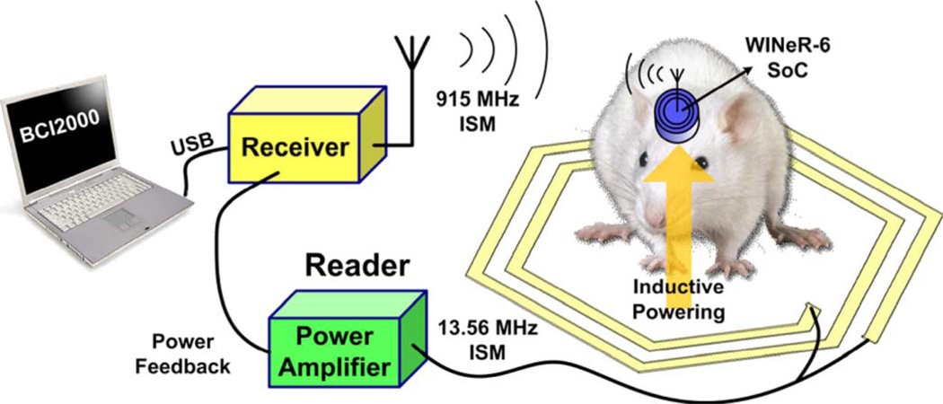
Fig. 1 shows a conceptual view of the WINeR-6 system which employs two independent wireless links in the industrial-scientific-medical (ISM) band at 915 MHz and 13.56 MHz for wireless neural recording and inductive powering, respectively. The WINeR-6 SoC architecture has been described in Section II. The system operation has been divided into the neural signal flow and the inductive power flow, which are covered in Sections III and IV, respectively. An extensive set of simulation and measurement results is presented in Section V, followed by the concluding remarks.
Fig. 1.
Conceptual view of the inductively powered wireless-implantable neural recording system-on-a-chip (WINeR-6) for long-term neural recording from small freely behaving animals [10].
II. WINeR-6 Architecture
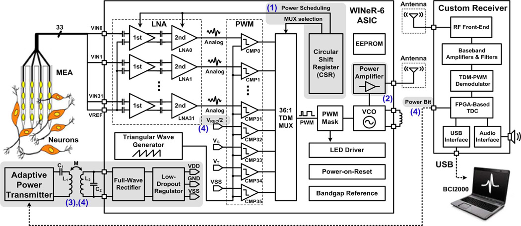
The current WINeR-6 system prototype consists of three key components: 1) a 32-channel transmitter application-specific integrated circuit (ASIC) that is integrated on a chip, 2) a custom designed wideband receiver unit (Rx), and 3) a wireless power transmitter unit (Reader). Fig. 2 shows the complete WINeR-6 system block diagram. Extracellular neural activity is picked up by a microelectrode array (MEA), which can be either micromachined or an equally spaced bundle of sharpened microwires. An array of two-stage low-noise amplifiers (LNA) magnifies the neural signals by a gain of up to 8000 [11]. An array of high-speed comparators compares the amplified neural signals with a precision triangular waveform to sample and convert their amplitudes to time segments in a step well known as pulse width modulation (PWM) or analog-to-time conversion (ATC) [12]. The next stage is a time-division multiplexer (TDM), which serializes the PWM samples and combines them with four monitoring signals: half of the rectifier output (VREC/2), bandgap reference voltage (VG), a temperature-dependent voltage (VT), and the negative supply rail (VSS).
Fig. 2.
WINeR-6 system block diagram with its key new features highlighted: 1) LNA power scheduling, 2) improved RF transmitter, 3) inductive powering, and 4) closed-loop power control [10].
Therefore, every frame of the PWM signal at the output of the TDM block consists of 36 pulses, which pass through a PWM mask to improve their timing accuracy (see Section III-E) and drive a tunable voltage-controlled oscillator (VCO) that operates around 915 MHz. The VCO upconverts the baseband PWM-TDM signal by frequency-shift keying (FSK) and, finally, the PWM-TDM-FSK signal at the output of the VCO is RF amplified and transmitted through a miniature wideband monopole antenna.
The custom-designed external wideband receiver, which is shown on the right side of Fig. 2 and a yellow box in Fig. 1, RF amplifies and downconverts the received PWM-TDM- FSK signal to a baseband PWM-TDM. This signal is then fed into a time-to-digital converter (TDC), which has been implemented on a field-programmable gate array (FPGA) [12]. The result is a series of digitized samples from the recorded neural signals, which are sent to a PC through its universal-serial-bus () port to be demultiplexed into individual waveforms before further digital signal processing, storage, and visualization in the BCI2000 environment [13].
The WINeR-6 system has four important new features compared to its predecessor (WINeR-5): 1) LNA power scheduling; 2) an improved RF transmitter; 3) inductive powering; and 4) closed-loop power control, which are highlighted in Fig. 2 and explained in more detail in the following sections.
Our prior experience with WINeR-5 showed that although each LNA consumes a small amount of current, since there are 32 of them on-chip, the LNA block quickly becomes one of the major power consumers of the WINeR SoC. To address this issue, we have employed a power-scheduling mechanism that puts most of the LNAs that are not being sampled in sleep mode with very low power consumption. This is explained in more detail in Section III-D. In WINeR-6, we have added a class-AB RF power amplifier (PA) after the VCO in order to extend the transmission range, improve the signal-to-noise ratio (SNR) at the receiver input, and stabilize the VCO operation by blocking reflections and backscattering from the antenna. The external adaptive power transmitter, which is shown on the lower left corner of Fig. 2, and a green box in Fig. 1 drives a geometrically optimized hexagonal coil that induces power at 13.56 MHz in a receiver LC-tank circuit that is embedded in the animal headstage [14]. The induced power is sent to an on-chip active full-wave rectifier that is followed by a low dropout regulator. Thanks to the closed-loop power control mechanism, WINeR-6 is expected to maintain the power delivered to the headstage at a constant level even when the distance or alignment between the transmitter and receiver coils change due to animal movements [15], [16].
III. Neural Signal Flow
A. Low-Noise Amplifiers (LNAs)
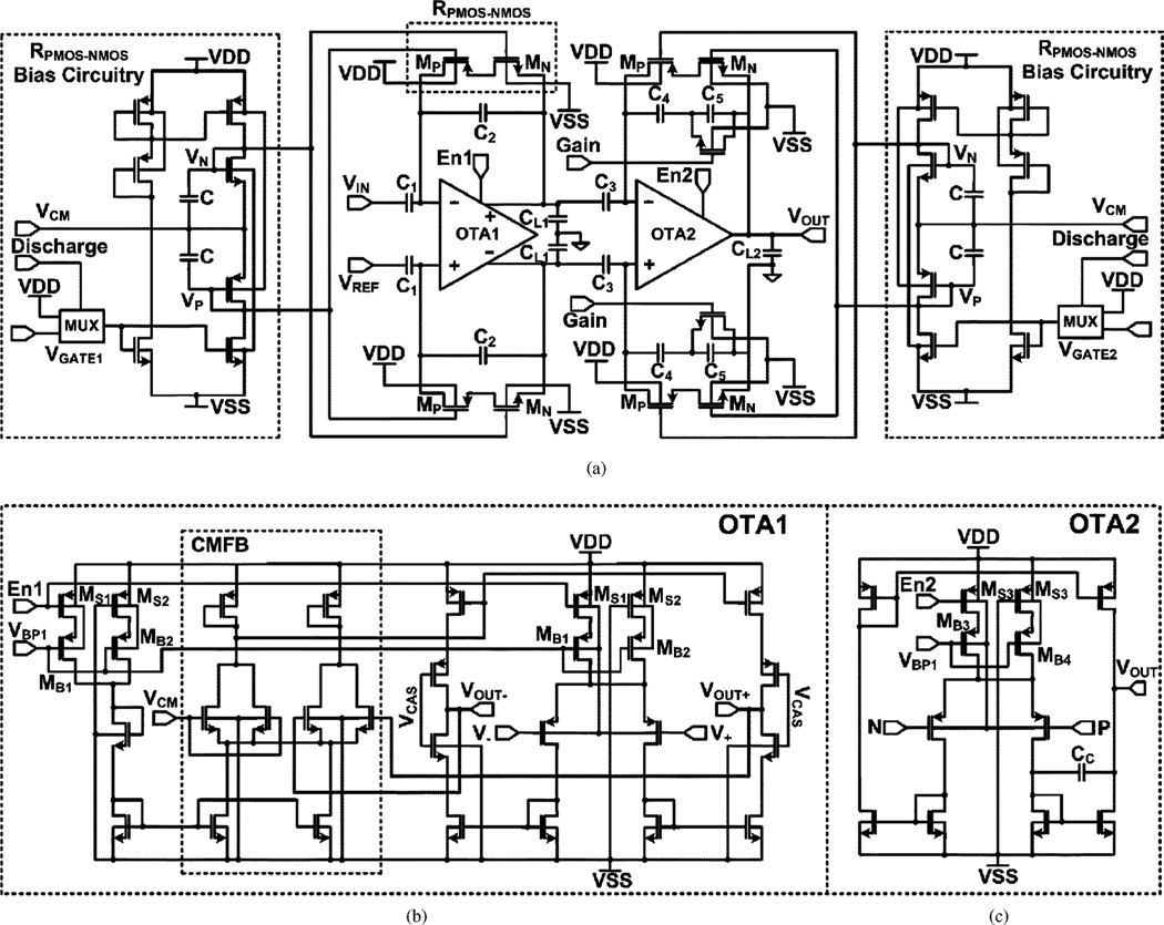
Extracellular neural signals that are picked up by the MEA have amplitude levels in the 50–500 µV range, a bandwidth of 0.1 Hz to 10 kHz, and large dc components due to electrode-electrolyte half-cell potentials [3]. The WINeR-6 analog front end has been designed accordingly, using two-stage capacitively coupled LNAs with built-in tunable bandpass filtering. The schematic diagram of the LNA is shown in Fig. 3. The first-stage LNA is a fully differential operational transconductance amplifier (OTA1), shown in Fig. 3(b), with a midband gain of C1/C2 = 100. VCM is the common-mode voltage usually tied to ground, and VREF is the reference voltage from the animal reference electrode. Turning OTA1 completely off when it is not in use in order to reduce power consumption results in a long transient to allow charge build up in its capacitors before it retains its normal operation. To reduce this transient time, we simply change theOTA1 bandwidth from its nominal value at 10 kHz when the current consumption is 16 µA (En1 = VSS) and the LNA is in the active mode to 200 Hz when the current consumption is ~ 0.5 µA (En1 = VDD), and the LNA is in sleep mode (also see Section III-D and Fig. 5). The second stage of the LNA (OTA2), shown in Fig. 3(c), has an adjustable gain of either C3/C4 = 20 or C3(C4 + C5)/(C4C5) = 80 for a total LNA gain of 2000 or 8000 (66/78 dB). The current in OTA2 also changes from 8.6 to 2.8 µA when the LNA is switched from the active to sleep modes, and vice-versa (controlled by En2).
Fig. 3.
Schematic diagram of the WINeR-6 analog front end. (a) Two-stage LNA. (b) OTA1. (c) OTA2.
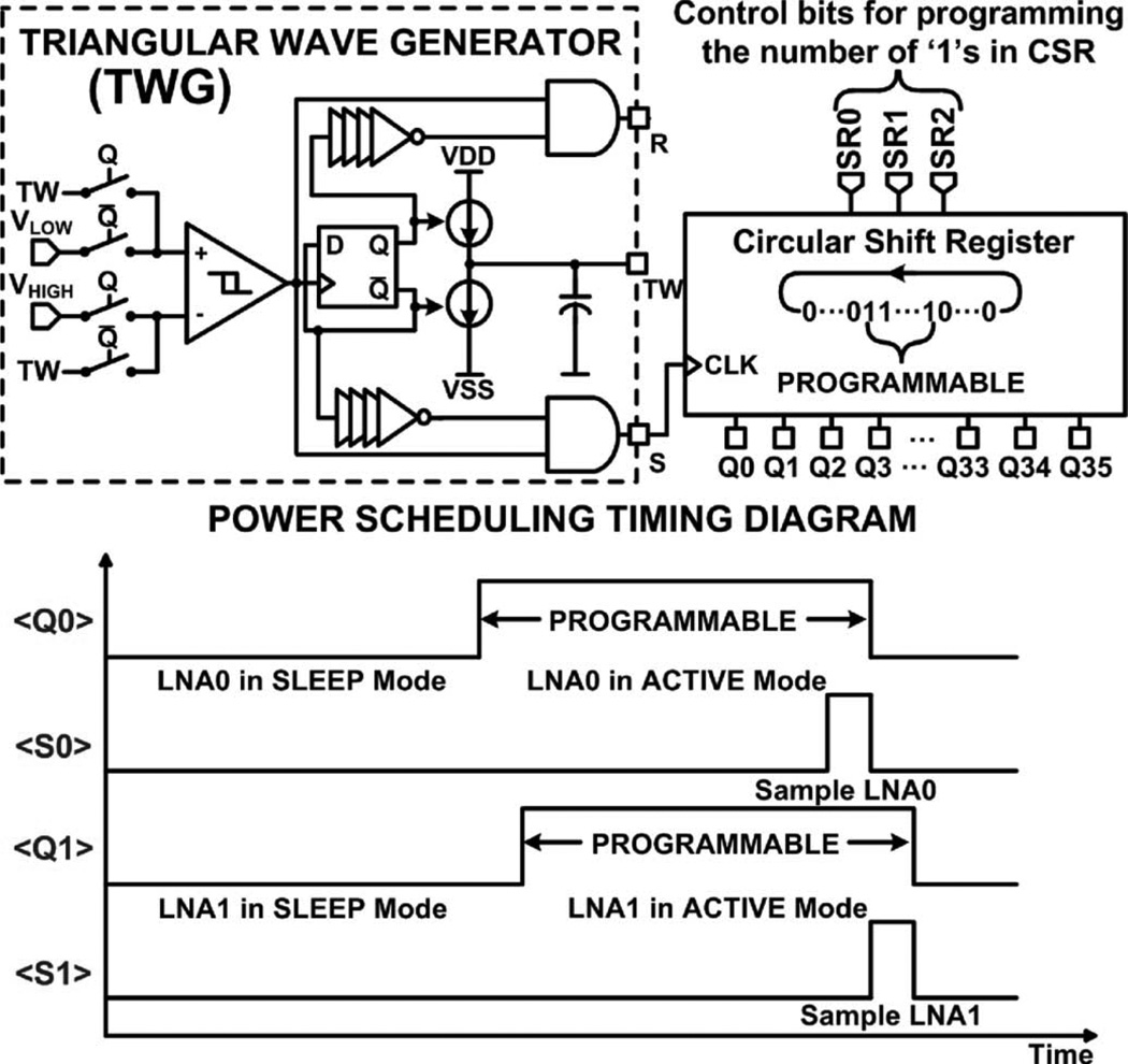
Fig. 5.
Block diagram and timing diagram of the power scheduling mechanism. The OTAs in the LNA block are switched between active (BW = 10 kHz) and sleep (BW = 200 Hz) modes by changing their bias currents.
Achieving low-cutoff frequency in the sub-hertz range with a small footprint on the chip is a challenge for LNA designers. Many have used subthreshold-biased MOS resistors or diode-connected MOS resistors to achieve high resistance (> 1011 Ω) and ultra low cutoff frequencies [17]–[19]. However, in these designs, the MOS resistance highly depends on the input and output voltages, causing distortion when large signals appear at the output. This is not uncommon, particularly at the output of OTA2 in the presence of local field potentials (LFP), which are inband neural signals from large populations of neurons firing in sync, and creating low-frequency signals with relatively large amplitudes.
To solve this problem, both stages of the LNA in Fig. 3(a) are equipped with voltage-controlled PMOS-NMOS pseudo resistors RPMOS-NMOS to create a low-cutoff frequency that can be continuously tuned by VGATE1 and VGATE2, as presented in [11]. RPMOS-NMOS transistors are biased with floating bias circuitry so that they can operate as a bidirectional current source. Hence, the impedance seen from either end of the RPMOS-NMOS remains constant and almost independent of the OTA input and output voltages, causing less distortion.
B. Pulsewidth Modulator and 36:1 Time-Division Multiplexer
As shown in Fig. 2, conditioned neural signals at the 32 LNA outputs join four monitoring signals: VREC/2, VBG, VT, and VSS at the input of the PWM-TDM block. These 36 analog signals are fed into the PWM block, which consists of 36 rail-to-rail high-speed comparators, enabled one at a time over one sampling period, to convert the analog signals from each channel into a sequence of pulses by comparing them with a precision triangular waveform (TW). To reduce noise and dynamic power dissipation, WINeR-6 does not use any high frequency clock signal. Instead, it uses a low-frequency clock at the sampling rate for TDM, which is generated locally by the triangular waveform generator (TWG) block. As a result during each comparison, the substrate is entirely quiet and there is no digital transition anywhere on the chip. Monitoring signals also play a second role by providing a unique pattern that is used for synchronization between the WINeR-6 transmitter and external receiver by marking the beginning of each TDM-PWM 36-pulse frame to be easily detected on the receiver side.
The TDM block consists of a 36-b circular shift register (CSR) and a 36:1 multiplexer (MUX) as shown in Fig. 5. The CSR receives a buffered time-base signal at the sampling rate from the TWG block, shown in Fig. 4 for its clock. At the global reset, the CSR is loaded with a 36-b binary code “1…10…00,” in which the number of “1”s is programmable (N). When the system is running, the string of “1”s circulates in the CSR and connects one out of 36 comparator PWM pulses (the last “1”) to the MUX output. The resulting signal will be a 36-pulse TDM-PWM frame, which is buffered and trimmed before being fed into the VCO. The architecture shown in Fig. 2 significantly facilitates the extension of the WINeR-6 system from 32 to 64 or 128 channels.
Fig. 4.
Schematic diagram of the triangular waveform generator (TWG) block.
C. Triangular Waveform Generator (TWG)
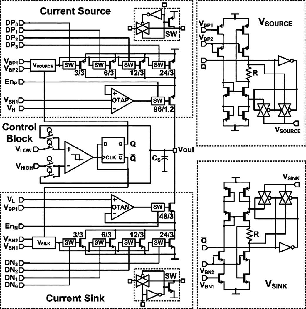
Precision TWG, shown in Fig. 4, is a key building block in accurate ATC. Its performance affects noise, accuracy, and resolution of the system, as described in [12]. The TWG consists of a binary weighted (DP0~3 and DN0~3), high-voltage compliance (−1.4 ~ 1.4 V), large output impedance, complementary current source/sink (CCSS) pair, which linearly charges/discharges CS (6 pF) to generate the triangular wave [8], [20]. Unlike common designs that need at least two comparators, our new TWG design utilizes only one comparator to reduce power consumption and the negative effects of offset mismatch. VSource and VSink are dynamic, current limited, bias generator blocks. They provide fast switching waveforms at specific dc biasing nodes to turn the CCSS on and off, while consuming negligible static power.
D. Power Scheduling
Although each individual LNA consumes only ~ 25 µA, the 32-channel LNA block is responsible for 42% of the total WINeR-6 power consumption when all channels are active. Unfortunately, this situation only gets exacerbated with an increased number of channels. On the other hand, the TDM-PWM block, described in Section III-B, only samples one LNA at a time. To address this issue, we have employed a power scheduling mechanism, depicted in Fig. 5, which puts most of the LNAs that are not being sampled in the sleep mode, where their power consumption reduces by 86% to ~ 3.5 µA.
The LNAs are not completely turned off to reduce the transient time tT for a dormant LNA to reach its active state well ahead of the sampling time to track the neural signals with high bandwidth and low distortion (10 kHz). Since tT cannot be reduced down to zero, the number of LNAs that should be activated ahead of sampling, N, depend on the overall sampling rate fS, which, in turn, depends on the desired neural signal bandwidth (i.e., N > fStT). In our design, N is programmable by SR0:2, which can change the number of consecutive “1”s in the CSR from 4 to 32. For example, when N = 12, twelve consecutive “1”s circulate in the CSR and each LNA is switched to the active mode 11 times the sampling period 11/fs, before being sampled. In this case, LNAs remain in the sleep mode during the rest of the sampling periods (24/fs) and result in more than 51% reduction in power consumption of the LNA block.
E. PWM Mask
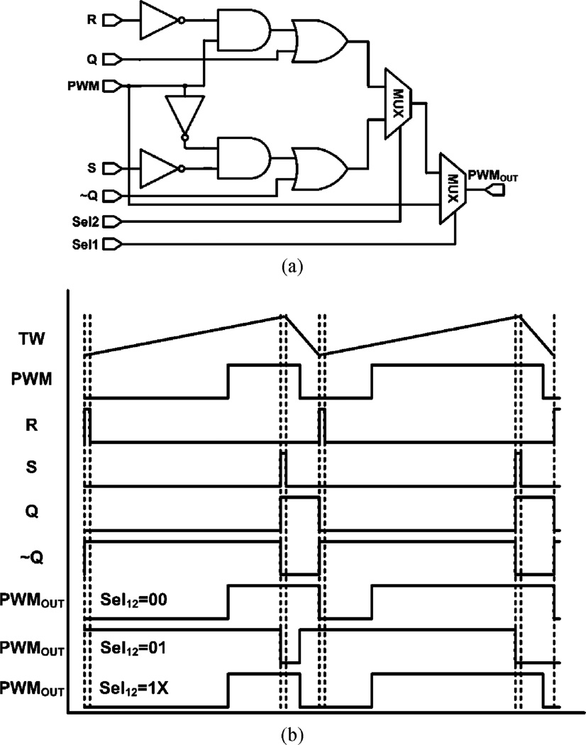
Fig. 6(a) shows the schematic of the PWM mask that is responsible for enforcing minimum and maximum PWM pulsewidths. This circuit reduces the wireless-link bandwidth requirements and increases the system accuracy by avoiding high and low PWM pulses that are too narrow. In addition, it synchronizes the PWM signal at the falling edges of Q or ~ Q. Fig. 6(b) shows the PWM mask operation and its associated signals. PWM is the signal before trimming and synchronization, and R, S, Q, and ~ Q are generated by the TWG block in Fig. 4. Sel1,2 are user-defined digital inputs. When Sel1,2 = 00, the PWM mask output will be synchronized with the falling edge of Q (PWM1), with maximum and minimum pulsewidths of ~ R and Q, respectively. When Sel1,2 = 01, the output of the PWM mask will be synchronized with the falling edge of ~ Q (PWM2), with maximum and minimum pulsewidths of ~ S and ~ Q, respectively. Finally, when Sel1,2 = 10 or 11, the PWM mask is bypassed (i.e., PWM3 = PWM).
Fig. 6.
(a) Schematic diagram of the PWM mask circuit. (b) PWM mask waveforms.
F. Voltage-Controlled Oscillator and Power Amplifier
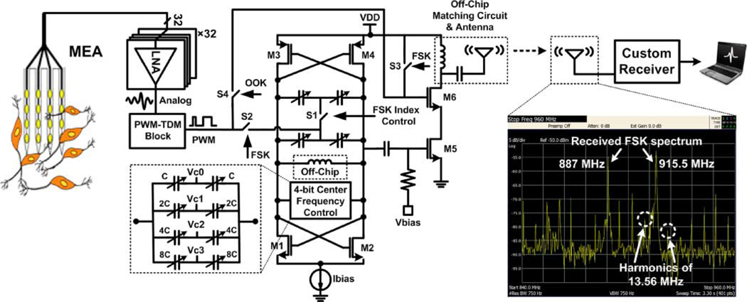
The WINeR-6 RF transmitter consists of a VCO with an off-chip inductor followed by a PA, as shown in Fig. 7. Animal movements in the shielded Faraday cage resulted in undesired VCO frequency shifts in WINeR-5 due to changes in the antenna loading and reflected RF signal. To prevent this, a nonlinear class-AB PA is used to not only reduce the frequency-shift problem but also help with the transmitter output matching with miniature 50-Ω antennas, and extend the transmission range. A complementary negative-Gm structure is used for the VCO core due to its low power and superior phase-noise performance [21]. Coarse and fine VCO tunings are performed with the choice of an off-chip inductor and a 4-b on-chip varactor bank (VC0:3), respectively. The VCO varactors are PMOS transistors, in which the gates are connected to the VCO outputs, bulks are tied to VDD, and sources and drains are tied together and connected to either the varactor bank control signals (VC0:3) for center frequency tuning or the TDM-PWM signal to generate the FSK signal. In order to fine tune the transmitter frequency, VC0:3 is accessible to the user. Once the VCO frequency is adjusted in the desired band, the external receiver can be tuned to the transmitter frequency.
Fig. 7.
WINeR-6 neural signal-flow diagram with emphasis on the transmitter SoC.
G. Custom-Designed Wideband Receiver and BCI2000
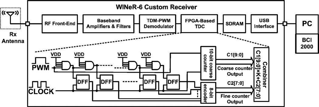
The external custom-designed wideband receiver in the WINeR-6 system is responsible for amplifying the received RF signal, downconverting it, FSK demodulating it back to the baseband TDM-PWM signal, digitizing the PWM samples taken from the neural signals, and sending this information to a PC for demultiplexing, storage, visualization, and real-time or offline processing. The receiver block diagram is shown in Fig. 8, where the key blocks are: RF front end, FSK demodulator, TDC, continuous high-data-rate USB interface, and real-time graphic user interface (GUI). In the RF front end, the received FSK-TDM- PWM carrier is amplified and bandpass filtered by a wideband RF LNA and a surface-acoustic-wave (SAW) filter, respectively. A mixer downconverts the carrier signal from RF to intermediate frequencies (IF), and power stabilizes it within ±0.5 dB by its automatic gain controller (AGC). The IF-TDM- PWM is then rectified and low-pass filtered with selectable receiver bandwidths (BW = 9/18/36 MHz) to recover the baseband TDM-PWM signal. The rising and falling edges of the TDM-PWM signal are sharpened by a high-speed comparator to improve the timing accuracy [12].
Fig. 8.
Block diagram of the custom-designed external wideband receiver.
An FPGA-based TDC with 308-ps time resolution converts the TDM-PWM pulses into a series of 16-b digitized samples. It also buffers them through 2-MB SDRAM to maintain the continuity of the signal despite data-transfer delays, and sends them to a PC via its 2.0 port for visualization, storage, and further processing [22]. In the PC, continuous real-time data demonstration was performed in the BCI2000 environment, which is general-purpose open-source software for brain–computer interfacing (BCI) research applications [13].
IV. Inductive Power Flow
Key components that are responsible for inductively powering the WINeR-6 system are similar to those used in radio-frequency-identification (RFID) systems: inductive power transmitter, inductive link, and the transponding portion of the WINeR-6 SoC, as shown in Fig. 9. On the power transmitter side, which can also be referred to as the reader or interrogator, a power amplifier drives the primary coil (L1) at the power carrier frequency of fc = 13.56 MHz. We chose this frequency, which is closer to the higher end of the 1~20 MHz acceptable range for implantable microelectronic devices (IMD), to enhance the quality factor of the coils Q, which improves the power transfer efficiency. Another reason was to take advantage of the commercial off-the-shelf (COTS) devices that are available for RFID applications for building the reader.
Fig. 9.
Inductive closed-loop power-flow diagram.
The power carrier is induced on to the secondary coil (L2), and generates ac voltage across the transponder resonance circuit (L2 and C2). Following the L2C2 tank, there is a full-wave rectifier and a low dropout regulator to generate VREC and supply lines, respectively, for the rest of the WINeR-6 SoC. To implement efficient and robust inductive power flow, the following techniques were employed: 1) full-wave active rectification using high-speed comparators to improve the power conversion efficiency (PCE), 2) closed-loop power control to maintain the supply voltage constant despite the coils’ coupling variations, and 3) an optimized coil design to maximize the power transmission through the inductive link.
A. Full-Wave Active Rectifier
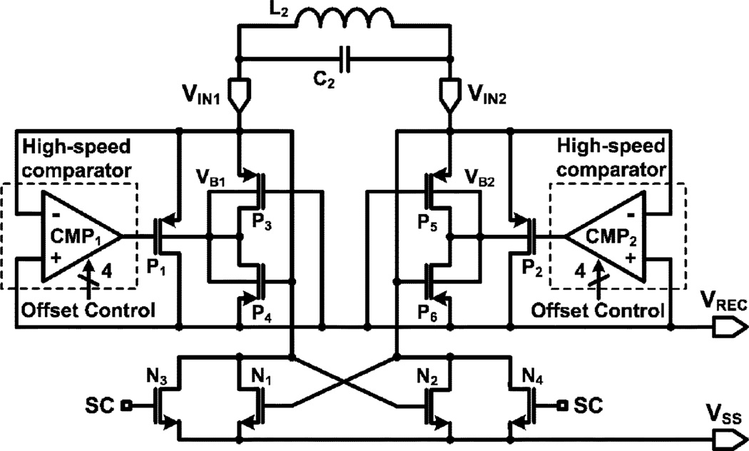
The performance of the rectifier is key to the overall power efficiency of this system because all of the usable received power for the WINeR-6 SoC has to pass through this block. Achieving a high PCE is generally important in inductively powered IMDs because it allows them to operate with smaller induced power from a longer distance, lowering the heat dissipation on both sides of the inductive link, which can cause tissue damage if it results in temperature rise beyond safe limits [23]. We utilized a full-wave active rectifier, shown in Fig. 10, which is equipped with offset-controlled high-speed comparators (CMP1 and CMP2) that provide high PCE at a high frequency (13.56 MHz). The offset-control function in these comparators compensates for turn-on and turn-off delays in operating the main rectifying switches (P1 and P2) and closes or opens them precisely when VIN1,2 > VREC or VIN1,2 ≤ VREC, respectively. As a result, the rectifier conducts for the maximum possible period of time and delivers maximum forward current to the load, while minimizing the back current. The comparator has a common-gate input stage (see further details in [24]), in which the two comparator input voltages are also used as supply voltages. Hence, the sinusoidal input voltage (VIN1,2) guarantees that the rectifier reliably starts up even before the rectifier output voltage (VREC) is sufficiently charged up. In addition, the rectifying transistor sizes were optimized for minimizing their Ron and switching losses at the rectifier operating frequency (13.56 MHz) by detailed PCE analysis [24], [25].
Fig. 10.
Schematic diagram of the power-efficient full-wave active rectifier.
In addition, the rectifier block has a built-in back telemetry mechanism, using short-coil switches N3 and N4 that can be utilized for reverse data communication with the reader in order to establish a closed-loop control mechanism for wireless power transmission (see Section IV-B). WINeR-6 SoC has also been equipped with a detuning-based overvoltage protection circuit, shown in Fig. 9, which is a necessary safety feature for situations in which the rectifier input signal has grown too large as a result of the coils being too close or the load current being too small. The overvoltage protection circuit compares VREC/4 with VREF = 1.1 V, and if VREC > 4.4 V, closes a switch that adds a 120-pF off-chip capacitor in parallel with C2. This will detune the L2C2 tank and reduce the rectifier input voltage, and consequently reduce VREC to the safe limits without heat dissipation that often results from voltage clamping methods.
B. Closed-Loop Power Control Mechanism
The heart of the external power transmitter in Fig. 9 is a COTS 13.56-MHz RFID reader (MLX90121) from Melexis (Concord, NH). It drives a class-C PA that is added to increase the RFID maximum output power from 200 mW to 1 W. The PA supply voltage has been used to control its output power through a Darlington-connected BJT pair for closed-loop power control [26]. The reader adjusts the transmitted power by monitoring VREC/2, which is one of the four monitoring signals that are added to each PWM-TDM frame (see Section II) and fed back to the external receiver. The idea is to oppose any undesired variations in VREC due to changes in the coils’ coupling coefficient k, resulting from animal movements or load variations, due to changing N for example.
A control unit, which consists of an MSP430, an 8-b DAC, and the Darlington pair, as shown in Fig. 9, adjusts the transmitted power with an adjustable step size, until VREC reaches its nominal value. Therefore, in steady state, the control unit adjusts the transmitted power to ensure that a constant amount of power is being delivered to the WINeR-6 SoC, and VREC is maintained around 3.2 V. In the presence of a disturbance, often in the form of a change in the coils relative distance, alignment, or rotation, VREC deviates from its nominal value, and the control unit counter inside MSP430, which is driven by a 100 Hz clock, counts up or down based on the received VREC value to bring VREC back to 3.2 V. In this implementation, the digital-to-analog converter (DAC) in the power-control loop can change the PA supply voltage from 2 V to 12 V in 256 steps.
C. Optimized Coil Design
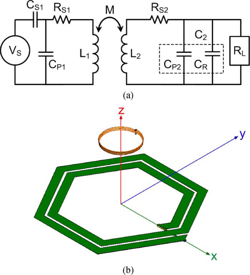
A simplified model of the inductive power transmission link is shown in Fig. 11(a). L1 is the primary with a hexagonal planar spiral coil (PSC) geometry, which is placed at the bottom of a small cage. L2 is going to be another PSC or a solenoid-type secondary coil that is wound around the animal headstage (see Fig. 1). All windings have distributed parasitic resistance and capacitance associated with them, which are shown as lumped elements RS1, RS2, CP1, and CP2 in Fig. 11(a). CS1 and CR are additional capacitors that are added to the circuit to form a pair of resonance LC-tank circuits with L1 and L2, respectively, and RL represents the loading of the WINeR-6 SoC. The values of these lumped elements are dependent on the coils’ geometry and material properties. For instance, the inductance of a PSC from [27] can be found from
| (1) |
| (2) |
where n is the number of turns, do and di are the outer and inner diameters of the coil, respectively, davg = (do + di)/2, and φ is a parameter known as the fill factor. Detailed modeling of the parasitic capacitance (CP1) and resistance (RS1) of PSCs has been discussed in [14] and [28].
Fig. 11.
(a) Simplified model of the inductive link with lumped circuit components. (b) More detailed modeling of the primary PSC at the bottom of the cage and the secondary solenoid, embedded in the headstage, using the HFSS commercial field solver.
The inductance model for a solenoid can be found from [29]
| (3) |
| (4) |
where Mab is the mutual inductance from (5) between turn a and turn b, La is the self inductance of turn a, and Dcond and OD are the diameters of the conductor and a single turn of the solenoid, respectively. Maxwell equations are used for deriving Mij between a pair of parallel single-turn circular coils at radii ri and rj from
| (5) |
where D is the relative coupling distance between the two coils and γ is the lateral misalignment [29], [30]. J0 and J1 are the Bessel functions of the zeroth and first order, respectively.
Since the received power decreases when the coupling distance increases, the coil geometries should be optimized for the worst case conditions to maintain minimum–received power at all times. However, considering all possible worst case scenarios that can arise from animal movements, such as when the animal turns its head or stands on its hindlimbs, requires a very complicated analysis, which is out of the scope of this paper. Therefore, we have optimized the coil geometries for a much simpler condition when the nominal coupling distance between the primary PSC and the headstage, mounted on top of a rat’s head is ~7 cm. The idea is that any further misalignments or changes in the coils’ separation will be compensated by the closed-loop power control mechanism (see Section IV-B). With these assumptions and the above models, the optimal geometry of the coils can be found by following the iterative design methodology that was described in [14]. In this method, although the closed-form theoretical models in (1)–(5) provide a quick estimate of the suitable coil geometries, more accurate models are utilized in a commercial field solver, HFSS (Ansoft, Pittsburgh, PA), to fine tune the optimal coil designs. Fig. 11(b) shows an example of these models.
V. Simulation and Measurement Results
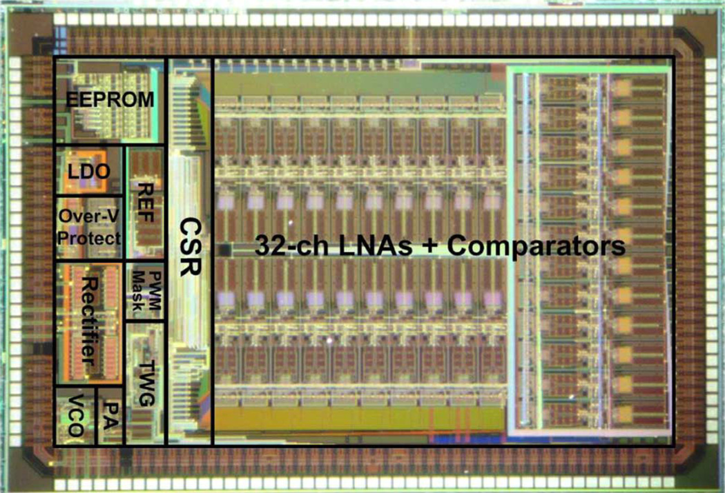
WINeR-6 SoC was fabricated in the ON Semiconductor 0.5-µm 3-metal 2-poly standard CMOS process. Fig. 12 shows the micrograph and floorplanning of the chip, which occupies 4.9 × 3.3 mm2 of silicon area, including the padframe.
Fig. 12.
Die photomicrograph of the 32-ch WINeR-6 SoC, implemented in the ON semiconductor 0.5-µm 3M2P std. CMOS process (size: 4.9 × 3.3 mm2).
A. WINeR-6 Bench-Top Characterization
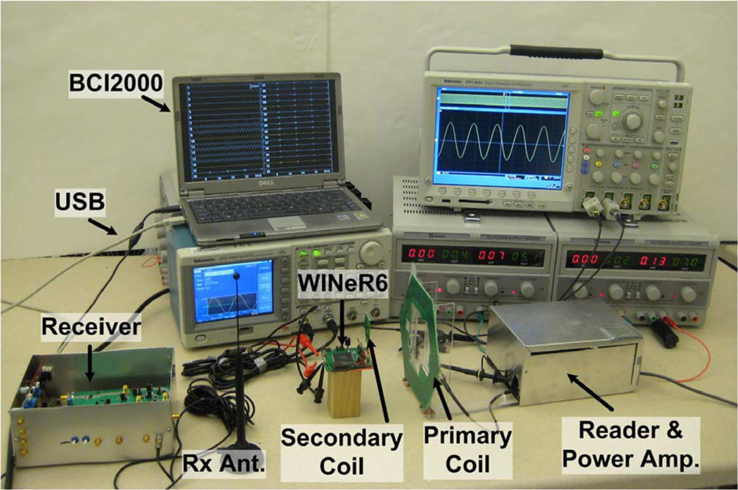
Fig. 13 shows our bench-top measurement setup, which includes the WINeR-6 SoC in a 176-pin TQFP package, mounted on a prototype printed-circuit board (PCB) along with the secondary coil and a small (17.6 mm) 916-MHz antenna (Antenna Factor, Merlin, OR). The setup also includes the hexagonal primary coil, connected to the reader box, as well as the external receiver box, connected via to a laptop PC that runs the BCI2000 GUI. The two coils were aligned at ~7 cm separation. The supply voltage of the class-C power amplifier, inside the reader box, was gradually increased by the closed-loop system until VREC on the WINeR-6 SoC reached its nominal value at 3.2 V.
Fig. 13.
Bench-top measurement setup (relative positions are changed to fit all components in the image).
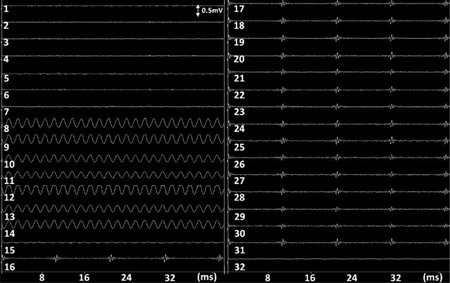
The FSK-TDM-PWM RF carrier signal was picked up at ~ 1 m away from the WINeR-6 SoC by a 26.2-cm receiver antenna that was designed for the 824~960 MHz band. The receiver amplified and downconverted the RF carrier to the 40/58 MHz IF-FSK-TDM-PWM, and rectified and filtered it to achieve a baseband TDM-PWM signal with 18-MHz bandwidth. It was then translated to transistor-transistor-logic (TTL) levels by a fast comparator and sent to the FPGA-based TDC for digitization. The 16-b digitized samples were buffered, packetized, and sent to the PC through as a stream of data, where the BCI2000 GUI demultiplexed them, stored them on the hard disk, and displayed them on the PC screen, as shown in Fig. 14. The 32-channel simultaneously recorded signals in Fig. 14 are wirelessly recorded when Ch1~7, Ch15, and Ch32 were grounded, Ch8~14 received sinusoidal waveforms of ~ 100 µVpp at 600 Hz, and Ch16~31 received attenuated artificial ECG signals at 120 Hz.
Fig. 14.
Simultaneous 32-ch bench-top wireless recording with inductively powered WINeR-6 system at 1 m Tx-Rx distance (BCI2000 GUI).
The first and second stages of the front-end LNA have measured gains of 40 dB and 27.8/38 dB, respectively. The lower cutoff frequency (i.e., high-pass filter) was continuously tunable from 0.1 Hz to 1 kHz. The higher cutoff frequency (i.e., low-pass filter) was 8 kHz at full-scale tail current. The fully differential design of the LNA leads to 62.7-dB power-supply rejection ratio (PSRR) and 134-dB common-mode rejection ratio (CMRR) in simulations, with a measured input-referred noise of 4.39 µVrms in 0.1 Hz–10 kHz when the system was battery powered.
The sampling frequency fS was adjustable in 225 steps from 58 kHz to 709 kHz using DP0~3 and DN0~3 digital inputs. The FSK modulation index of the RF carrier was adjustable by one bit. Therefore, the RF FSK carrier frequency of the application-spcific integrated circuit (ASIC) could be set to either 915/845.5 MHz or 915/877.5 MHz. The RF transmitter output power could reach −22 dBm with proper matching, in which case the Tx-Rx antenna distance could be as far as 3.3 m with inductive powering. Even though WINeR-6 does not transmit any digital bit per se, considering its transmitter power consumption of 3.3 mW, sampling rate of 680 kS/s, and system resolution of ~8 b, the equivalent energy per bit for its wireless data link can be calculated as 607 pJ/b. The maximum rectifier PCE was measured to be 80.2%, and the aligned coils’ separation could be increased up to 12 cm. Table I summarizes the measured key specifications of the WINeR-6 system, and Table II benchmarks its performance against the state of the art.
TABLE I.
Summary of WINeR-6 System Specifications
| Wireless Integrated Neural Recording System (WINeR-6) | ||
| Fabrication technology | ON Semiconductor 0.5-µm 3M2P Std. CMOS | |
| Die size (mm2) | 4.93 × 3.33 | |
| Supply voltage (V) | ±1.5 | |
| Total power consumption (mW) | 7.05 (N=32)/5.85 (N=12) | |
| Sampling rate (kSps) | 58 ~ 709 | |
| Neural Recording | ||
| Power source | Battery | Inductive |
| Number of channels | 32 recording + 4 monitoring | |
| LNA gain (dB) | 67.8/78 | |
| LNA CMRR/PSRR (dB)* | 134/62.7 | |
| LNA input referred noise (µVrms) (1 Hz ~ 10 kHz) | 4.08 | 4.62 |
| System input referred noise (µVrms) (1 Hz ~ 10 kHz) | 4.32 | 4.95 |
| Estimated system resolution (bits) | 8.3 | 8.1 |
| LNA current consumption (µA)* | 25 | |
| LNA bandwidth | HPF: 0.1–1000 Hz LPF: 8 kHz | |
| RF Telemetry Link | ||
| FSK carrier frequency (MHz) | 915/845.5 or 915/877 | |
| VCO center frequency tuning (MHz) | 0 ~ 50 (16 steps) | |
| VCO and PA current consumptioon (mA) | 1.1 | |
| Tx RF output power (dBm) | −22 | |
| Max. Tx-Rx antenna distance (m) | 3.4 | 3.3 |
| Inductive Powering | ||
| Operating frequency (MHz) | 13.56 | |
| Rectifier Vout/Vin(Peak)/Vin(RMS) (V) | 3.12/3.55/2.41 | |
| Rectifier power conversion efficiency | 80.2% | |
| Distance between coils (cm) | 12 (Max.)/7 (Nominal) | |
| LDO dropout voltage (mV) | 150 | |
| LDO current consumption (µA)* | 24 (Simulation) | |
| Peak to peak ripple on VDD/VSS (mV) | 80 | |
| Primary coil diameter (cm)/Number of turns/inductance (µH) | 16.8/2/0.88 (L1) | |
| Secondary coil diameter (cm)/Number of turns/inductance (µH) | 3.0/2/0.41 (L2) | |
Simulated value
TABLE II.
WINeR-6 Benchmarking
| Reference | [31] | [2] | [32] | [4] | This Work |
|---|---|---|---|---|---|
| Total # of Channels | 64 | 100 | 128 | 32 | 32 |
| Simultaneous Channels | 2 | 1 | 128 | 32 | 32 |
| LNA Gain (dB) | 60 | 60 | 60 | 46 | 67.8/78 |
| Power Source | Inductively powered | Inductively powered | Battery powered | Battery powered | Inductively powered |
| Modulation | OOK | FSK | UWB | FSK | PWM/FSK/OOK |
| Data Carrier Frequency | 174 ~ 216 MHz | 915 MHz | 4 GHz | 3.7 ~ 4.1 GHz | 433/915 MHz |
| Power Carrier Frequency | 4 MHz/8 MHz | 2.765 MHZ | N/A | N/A | 13.56 MHz |
| Data Acquisition | Spike data reduction | Spike data reduction | data reduction/raw | Raw data | Raw data |
| Data rate | 2 Mbps | 157 kbps | 90 Mbps | 24 Mbps | 58 ~ 709 kSps |
| Resolution (bits) | 8 | 10 | 9 | 12 | 8.1 |
| Data link Energy per bit | N/A | 3185 pJ/b | 17.78 pJ/b | 1250 pJ/b | 607 pJ/b |
| Power supply (V) | 1.8 | 3.3 | 3.3 | 5 | 3 |
| Process | 0.5-µm CMOS | 0.6-µm BiCMOS | 0.35-µm CMOS | Discrete | 0.5-µm CMOS |
| Power consumption (mW) | 14.4 | 8 | 6 | 142 | 5.85 |
B. Load-Pull Measurements
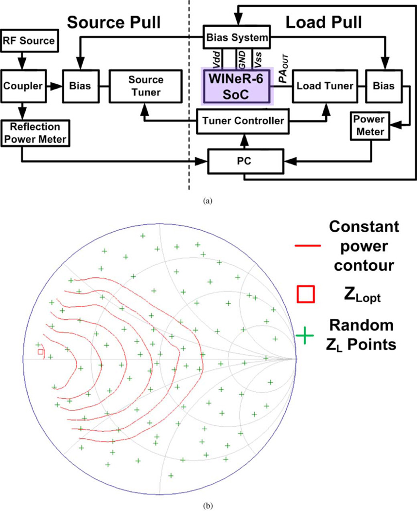
For nonlinear large signal devices, such as class-AB PAs, in which the operating point can change with the power level, conducting load-pull and source-pull measurements are necessary to find the optimum load and source impedances for transferring the maximum amount of RF power from source to load. We conducted load-pull measurements to find the optimum load, considering the parasitic effects of the bond wires, IC package, and PCB, while trying to keep the power consumption at its minimum level. The load-pull measurement setup has been shown in the form of a block diagram in Fig. 15(a), in which the source tuner was set to a fixed position, and load power was measured at a variety of randomly located load impedance points (ZL). WINeR-6 SoC was supplied by a bias generating system, which was controlled by a PC. The class-AB PA output (PAOUT) was also connected to the load tuner. Fig. 15(b) shows the selected random ZL points and constant output power contours in 1-dB steps on the Smith chart. The load-pull measurements showed that the maximum output power at a certain bias point is −21.7 dBm when the load impedance is 3.48 + j1.48. The matching circuit following the PA was then designed to convert the 50-Ω antenna to this optimum loading.
Fig. 15.
(a) Source and load-pull measurement setup. (b) Load-pull measurement results on the Smith chart.
C. Power Scheduling Measurements
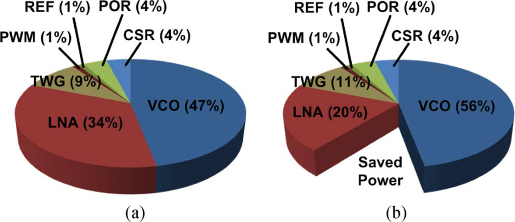
WINeR-6 power consumption with and without power scheduling has been compared in Fig. 16. When all LNAs are active, WINeR-6 consumes 7.05 mW from ±1.5-V supplies. On the other hand, when 12 LNAs are on (N = 12) at a time and the other 20 are in the sleep mode by power scheduling, power consumption drops by 17% to 5.85 mW. From a different perspective, depicted in Fig. 16, with power scheduling, the share of the LNA block power consumption in the total power consumption reduces from 34% to 20%. Obviously, this power saving becomes even more significant by decreasing N. However, if N < fStT, LNA outputs will be sampled before they reach their operational values, and that may cause distortion.
Fig. 16.
Comparison between the power consumption of each block in WINeR-6 SoC as the percentage of the total power with and without power scheduling, which results in 17% reduction in the total power consumption. (a) Without power scheduling 7.05 mW. (b) With power scheduling of 5.85 mW.
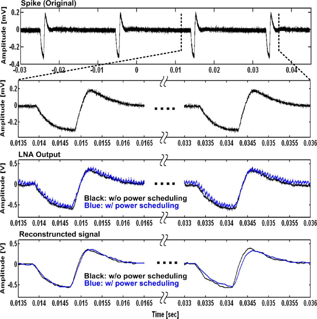
In order to evaluate the effect of power scheduling on the quality of the recorded signals, we applied artificial spikes with 0.5-mV amplitude and 1-ms pulsewidth to the LNAs inputs, and compared the recorded signals with and without power scheduling. Fig. 17 shows the measured waveforms, in which the sampling rate is set to 18 kS/s per channel, and N = 12. The upper two waveforms show the LNA inputs. In the third row, the black trace shows the output signal without using power scheduling, and the blue trace shows the output signal with power scheduling. Even though the LNA output seems to be noisy with power scheduling, since the LNA output reaches its operational value by the time each sample is taken, the effect of this noise on the digitized signal will be negligible. The last row shows the reconstructed signals from the digitized samples. The correlation coefficient between the two reconstructed signals was measured to be 0.97, which demonstrates almost a perfect match between the two conditions.
Fig. 17.
Measured waveforms from the top: Original artificial spike waveform, zoomed-in spike waveform, recorded waveforms at the LNA output with (blue) and without (black) power scheduling, reconstructed signal in the PC.
D. Closed-Loop Power Control Measurements
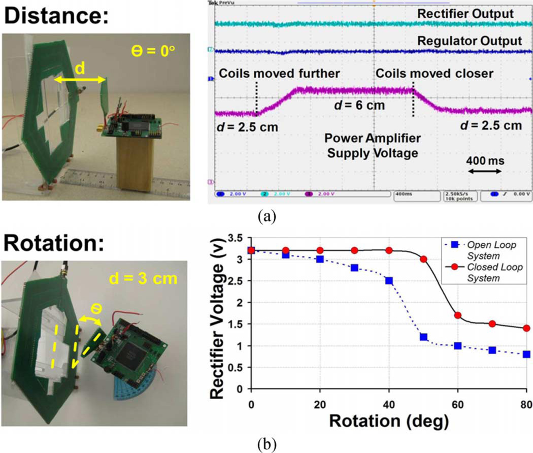
Functionality of the closed-loop induced power was verified by changing the distance d between L1 and L2. Fig. 18(a) shows VREC (green) and VREG (blue) outputs on the WINeR-6 SoC as well as the PA supply voltage on the reader side (purple). When d = 2.5 cm, the PA supply is 7 V, VREC = 3.2 V, and VREG = 3 V. In about 600 ms after the beginning of the trace, d is suddenly changed to 6 cm, which results in the reduction of VREC. In the meantime, the closed-loop system monitors the reduction in VREC and starts increasing the PA supply voltage to 10 V to oppose this perturbation and bring VREC back to 3.2 V. The coils are then returned back to their original position at d = 2.5 cm after 2.4 s, resulting in the PA supply voltage to return back to 7 V.
Fig. 18.
(a) Measured waveforms showing the constant rectifier (VREC = 3.2 V) and regulator (VREG = 3 V) outputs when the coils’ relative distance varies from 2.5 cm to 6 cm, and back to 2.5 cm. (b) Measured VREC versus the rotation angle of L2 with respect to L1 at d = 3 cm.
The key point here is that during all of these changes, the regulator voltage was maintained constant at 3 V. Fig. 18(b) shows the effect of the closed-loop power control on the rotation of L2 with respect to L1 at d = 3 cm. In this case, it can be seen that the closed-loop system can tolerate rotations up to 50° with no change in VREC.
E. Noise Measurements and System Resolution
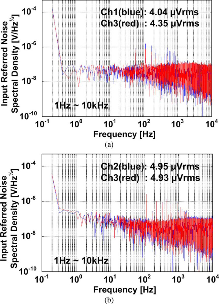
In data-acquisition systems, such as WINeR, the dynamic range of the front-end stage and noise performance of the entire system affects the system resolution and accuracy [12]. Noise is being added to the input signal at every stage along the signal path in Fig. 2 from the LNA to TDC output. The LNA input-referred noise in the 1 Hz to 10 kHz range was measured to be 4.08 µVrms and 4.62 µVrms when the system was battery and inductively powered, respectively. We also measured the input-referred noise by directly feeding the PWM-TDM signal to the TDC of the receiver through an isolator and bypassing the RF link. The input-referred noise in this case was 4.18 µVrms and 4.82 µVrms when the system was battery and inductively powered, respectively. We finally measured the input-referred noise of the entire 32-channel WINeR-6 system by grounding all channels and conducting fast Fourier transform (FFT) on the recorded data from all channels for 2 s at 120 cm Tx-Rx separation and 7-cm coil distance. The resulting input-referred noise spectral densities are shown in Fig. 19. Integration of these curves from 1 Hz to 10 kHz resulted in an input-referred noise of 4.32 µVrms and 4.95 µVrms on average when WINeR-6 was battery and inductively powered, respectively. Comparing these numbers, we can conclude that the input-referred noise of the entire system has been increased by 2.42 µVrms as a result of being inductively powered. This is mainly because of the RF link being affected by the higher harmonics of the strong power carrier, shown in the Fig. 7 inset. Also, considering 2.8-V dynamic range at the LNA output and its gain of 2000, the WINeR-6 system resolution can be estimated to be 8.4 b when it is hardwired, and about 8.3 or 8.1 b, when it is wireless and battery or inductively operated, respectively.
Fig. 19.
Input-referred noise of the entire WINeR-6 system for two channels, when the system is either (a) battery or (b) inductively powered. The Tx-Rx antenna distance is 120 cm, and the coils separation is about 7 cm.
VI. Conclusion
An inductively powered wireless-implantable neural recording system (WINeR-6), which can simultaneously record from 32 channels for an unlimited period of time has been presented. In this system, closed-loop inductive power control with optimal coil designs provides high-power transfer efficiency and maintains the received power at the headstage despite animal movements. The TDM-PWM-based architecture that is used in this system does not need an on-chip high-frequency clock and makes it easy to adjust the sampling rate, dynamic range, and resolution of the system based on the desired input signals and application. In addition, the total power consumption has been reduced using a power scheduling scheme, which keeps the majority of the LNAs in sleep mode. We have also developed all of the external components of the inductively powered wireless neural recording system including a wideband receiver, power transmitter (using an RFID reader), and computer interfacing hardware/software for real-time high throughput DAQ. Bench-top measurements showed that the system is fully functional by wirelessly recording 36 signals, simultaneously, including 32 external sources and 4 internal monitoring signals, sampled at 680 kS/s with more than 8 b of resolution at 1-m Tx-Rx distance, when WINeR-6 was inductively powered.
Acknowledgment
The authors would like to thank members of the GT-Bionics Laboratory for their help with the design and testing of the WINeR system.
This work was supported in part by the National Institutes of Health, NIBIB under Grant 1R21EB009437-01A1 and in part by the National Science Foundation under Award ECCS-824199.
Biographies

Seung Bae Lee (S’08) received the B.S. degree in electrical engineering from Hanyang University, Seoul, Korea in 2007 and is currently pursuing the Ph.D. degree at the Georgia Institute of Technology, Atlanta.
He came to the Georgia Institute of Technology in 2007 and joined the GT-Bionics Lab in 2008. He is working on an ultra-low-power RF receiver for biomedical and wearable applications as well as a wireless neural recording system.

Hyung-Min Lee (S’06) received the B.S. degree in electrical engineering (Hons.) from Korea University, Seoul, Korea, in 2006, the M.S. degree in electrical engineering from Korea Advanced Institute of Science and Technology (KAIST), Daejeon, Korea, in 2008, and is currently pursuing the Ph.D. degree from the Georgia Institute of Technology, Atlanta
Since 2009, he has been with the GT-Bionics Lab in the School of Electrical and Computer Engineering at the Georgia Institute of Technology. His research interests include analog, mixed-signal, and power-management integrated circuits for implantable biomedical systems.
Mr. Lee received the Silver Prize in the 16th Human-Tech Thesis Prize from Samsung Electronics, Korea, and the Commendation Award in the 4th Outstanding Student Research Award from TSMC, Taiwan, both in 2010.

Mehdi Kiani (S’09) received the B.S. degree at Shiraz University, Shiraz, Iran, in 2005 and the M.S. degree at Sharif University of Technology, Tehran, Iran, in 2008.
He joined GT-Bionics Lab at the Georgia Institiute of Technology, Atlanta, in 2009.

Uei-Ming Jow (S’07) received the B.E. degree in electrical engineering from Tatung University, Taiwan, in 1991, the M.S. degree in electronics engineering from National Taiwan University of Science and Technology, Taiwan, in 2001, and is currently pursuing the Ph.D. degree at the Georgia Institute of Technology, Atlanta.
From 2001 to 2006, he was with the Industrial Technology Research Institute (ITRI), Hsinchu, Taiwan, working in Electronics Research and Service Organization as an RF Engineer. He was involved in the analysis and design of electromagnetic compatibility for high-speed digital circuits as well as embedded RF circuits packaging technology. His main research interests are neural and bionic implants, integrated analog circuit design, and wireless-implantable biomedical systems.

Maysam Ghovanloo (S’00–M’04–SM’10) was born in 1973 in Tehran, Iran. He received the B.S. degree in electrical engineering from the University of Tehran, Tehran, Iran, in 1994, the M.S. degree in biomedical engineering from the Amirkabir University of Technology, Tehran, Iran, in 1997, and the M.S. and Ph.D. degrees in electrical engineering from the University of Michigan, Ann Arbor, in 2003 and 2004, respectively
From 2004 to 2007, he was an Assistant Professor in the Department of Electrical and Computer Engineering, North Carolina (NC) State University, Raleigh. In 2007, he joined the faculty of Georgia Institute of Technology, Atlanta, where he is currently an Assistant Professor and the Founding Director of the GT-Bionics Laboratory in the School of Electrical and Computer Engineering. He has authored or coauthored more than 70 peer-reviewed conference and journal publications.
Dr. Ghovanloo is an Associate Editor of the IEEE Transactions on Circuits and Systems–II: Express Briefs and a member of the Imagers, MEMS, Medical, and Displays (IMMD) Subcommittee at the International Solid-State Circuits Conference (ISSCC). He is the 2010 recipient of a CAREER award from the National Science Foundation. He has also received awards in the 40th and 41st Design Automation Conference (DAC)/ISSCC Student Design Contest in 2003 and 2004, respectively. He has organized several special sessions and was a member of Technical Review Committees for major conferences in the areas of circuits, systems, sensors, and biomedical engineering. He is a member of the Tau Beta Pi, AAAS, Sigma Xi, and the IEEE Solid-State Circuits Society, IEEE Circuits and Systems Society, and IEEE Engineering in Medicine and Biology Society.
Footnotes
Color versions of one or more of the figures in this paper are available online at http://ieeexplore.ieee.org.
References
- 1.Donoghue JP. Bridging the brain to the world: A perspective on neural interface systems. Neuron. 2008 Nov;60:511–521. doi: 10.1016/j.neuron.2008.10.037. [DOI] [PubMed] [Google Scholar]
- 2.Harrison RR, Kier RJ, Chestek CA, Gilja V, Nuyujukian P, Ryu S, Greger B, Solzbacher F, Shenoy KV. Wireless neural recording with single low-power integrated circuit. IEEE Trans. Neural Syst. Rehab. Eng. 2009 Aug;17(no. 4):322–329. doi: 10.1109/TNSRE.2009.2023298. [DOI] [PMC free article] [PubMed] [Google Scholar]
- 3.Schwartz AB, Cui XT, Weber DJ, Moran DW. Brain-controlled interfaces: Movement restoration with neural prosthetics. Neuron. 2006 Oct;52:205–220. doi: 10.1016/j.neuron.2006.09.019. [DOI] [PubMed] [Google Scholar]
- 4.Miranda H, Gilja V, Chestek CA, Shenoy KV, Meng TH. HermesD: A high-rate long-range wireless transmission system for simultaneous multichannel neural recording applications. IEEE Trans. Biomed. Circuits Syst. 2010 Jun;4(no. 3):181–191. doi: 10.1109/TBCAS.2010.2044573. [DOI] [PubMed] [Google Scholar]
- 5.Avestruz A, Santa W, Carlson D, Jensen R, Stanslaski S, Helfen-stine A, Denison T. A 5 μW/channel spectral analysis IC for chronic bidirectional brain–machine interfaces. IEEE J. Solid-State Circuits. 2008 Dec;43(no. 12):3006–3024. [Google Scholar]
- 6.Manns JR, Eichenbaum H. Evolution of declarative memory. Hippocampus. 2006 Sep;16(no. 9):795–808. doi: 10.1002/hipo.20205. [DOI] [PubMed] [Google Scholar]
- 7.Multichannel acquisition processor. Plexon Inc.; [Online]. Available: http://www.plexon.com/products/map.html. [Google Scholar]
- 8.Yin M, Ghovanloo M. A flexible 32-channel simultaneous wireless neural recording system with adjustable resolution; Proc. Dig. Tech. Papers IEEE Intl. Solid-State Circuits Conf; 2009. Feb, pp. 432–433. [Google Scholar]
- 9.Rizk M, Bossetti CA, Jochum TA, Callender SH, Nicolelis MAL, Turner DA, Wolf PD. A fully implantable 96-channel neural data acquisition system. J. Neural Eng. 2009 Apr;6(no. 2) doi: 10.1088/1741-2560/6/2/026002. art. 026002. [DOI] [PMC free article] [PubMed] [Google Scholar]
- 10.Lee SB, Lee HM, Kiani M, Jow U, Ghovanloo M. An inductively powered scalable 32-ch wireless neural recording system-on-a-chip with power scheduling for neuroscience applications; Proc. IEEE Intl. Solid State Cir. Conf. Dig. Tech. Papers; 2010. Feb, pp. 120–121. [DOI] [PMC free article] [PubMed] [Google Scholar]
- 11.Yin M, Ghovanloo M. A low-noise preamplifier with adjustable gain and bandwidth for biopotential recording applications; Proc. IEEE Int. Symp. Circ. Syst; 2007. May, pp. 321–324. [Google Scholar]
- 12.Yin M, Ghovanloo M. Using pulse width modulation for wireless transmission of neural signals in multichannel neural recording systems. IEEE Trans. Neural Syst. Rehab. Eng. 2009 Aug;17(no. 4):354–363. doi: 10.1109/TNSRE.2009.2023302. [DOI] [PMC free article] [PubMed] [Google Scholar]
- 13.BCI2000 Homepage. [Online]. Available: http://www.bci2000.org. [Google Scholar]
- 14.Jow U, Ghovanloo M. Design and optimization of printed spiral coils for efficient transcutaneous inductive power transmission. IEEE Trans. Biomed. Circuits Syst. 2007 Sep;1(no. 3):193–202. doi: 10.1109/TBCAS.2007.913130. [DOI] [PubMed] [Google Scholar]
- 15.Cong P, Chaimanonart N, Ko WH, Young DJ. Wireless and batteryless 10-bit implantable blood pressure sensing microsystem with adaptive RF powering for real-time laboratory mice monitoring. IEEE J. Solid-State Circuits. 2009 Dec;44(no. 12):3631–3644. [Google Scholar]
- 16.Kiani M, Ghovanloo M. An RFID-based closed loop wireless power transmission system for biomedical applications. IEEE Trans. Circuits Syst. II, Exp. Briefs. 2010 Apr;57(no. 4):260–264. doi: 10.1109/TCSII.2010.2043470. [DOI] [PMC free article] [PubMed] [Google Scholar]
- 17.Harrison RR, Charles C. A low-power low-noise CMOS amplifier for neural recording applications. IEEE J. Solid-State Circuits. 2003 Jun;38(no. 6):958–965. [Google Scholar]
- 18.Horiuchi T, Swindell T, Sander D, Abshire P. A low-power CMOS neural amplifier with amplitude measurements for spike sortingin. Proc. IEEE Int. Symp. Circ. Syst. 2004 May;4:29–32. [Google Scholar]
- 19.Olsson RH, III, Gulari MN, Wise KD. Band tunable and multiplexed integrated circuits for simultaneous recording and stimulation with microelectrode arrays. IEEE Trans. Biomed. Eng. 2005 Jul;52(no. 7):1302–1311. doi: 10.1109/TBME.2005.847540. [DOI] [PubMed] [Google Scholar]
- 20.Ghovanloo M, Najafi K. A compact large voltage compliance high output impedance programmable current source for biomedical implantable microstimulators. IEEE Trans. Biomed. Eng. 2005 Jan;52(no. 1):97–105. doi: 10.1109/TBME.2004.839797. [DOI] [PubMed] [Google Scholar]
- 21.Hajimiri A, Lee TH. A general theory of phase noise in electrical oscillators. IEEE J. Solid-State Circuits. 1998 Feb;33(no. 2):179–194. [Google Scholar]
- 22.Yin M, Ghovanloo M. A wideband PWM-FSK receiver for wireless implantable neural recording applications; Proc. IEEE Int. Symp. Circuits Syst; 2008. May, pp. 1556–1559. [Google Scholar]
- 23.Lazzi G. Thermal effects of bioimplants. IEEE Eng. Med. Biol. Mag. 2005 Sep-Oct;24(no. 5):75–81. doi: 10.1109/memb.2005.1511503. [DOI] [PubMed] [Google Scholar]
- 24.Lee H, Ghovanloo M. An integrated power-efficient active rectifier with offset-controlled high speed comparators for inductively-powered applications. IEEE Trans. Circuits Syst. I, Reg. Papers. doi: 10.1109/TCSI.2010.2103172. submitted for publication. [DOI] [PMC free article] [PubMed] [Google Scholar]
- 25.Bawa G, Ghovanloo M. Analysis, design and implementation of a high efficiency fullwave rectifier in standard CMOS technology. Analog Integr. Circuits Signal Process. 2009 Aug;60:71–81. [Google Scholar]
- 26.Kiani M, Ghovanloo M. A closed loop wireless power transmission system using a commercial RFID transceiver for biomedical applications; Proc. IEEE 31st Eng. Med. Biol. Conf; 2009. Sep, pp. 3841–3844. [DOI] [PMC free article] [PubMed] [Google Scholar]
- 27.Mohan SS, del Mar Hershenson M, Boyd SP, Lee TH. Simple accurate expressions for planar spiral inductances. IEEE J. Solid-State Circuits. 1999 Oct;34(no. 10):1419–1424. [Google Scholar]
- 28.Yang Z, Liu W, Basham E. Inductor modeling in wireless links for implantable electronics. IEEE Trans. Magn. 2007 Oct;43(no. 10):3851–3860. [Google Scholar]
- 29.Zierhofer CM, Hochmair ES. Geometric approach for coupling enhancement of magnetically coupled coils. IEEE Trans. Biomed. Eng. 1996 Jul;43(no. 7):708–714. doi: 10.1109/10.503178. [DOI] [PubMed] [Google Scholar]
- 30.Akyel C, Babic S, Kincic S. New and fast procedures for calculating the mutual inductance of coaxial circular coils (circular coil-disk coil) IEEE Trans. Magn. 2002 Sep;38(no. 5):2367–2369. [Google Scholar]
- 31.Sodagar A, Perlin G, Yao Y, Najafi K, Wise K. An implantable 64-channel wireless microsystem for single-unit neural recording. IEEE J. Solid-State Circuits. 2009 Sep;44(no. 9):2591–2604. [Google Scholar]
- 32.Chae MS, Yang Z, Yuce MR, Hoang L, Liu W. A 128-channel 6 mW wireless neural recording IC with spike feature extraction and UWB transmitter. IEEE Trans. Neural Syst. Rehab. Eng. 2009 Aug;17(no. 4):312–321. doi: 10.1109/TNSRE.2009.2021607. [DOI] [PubMed] [Google Scholar]


