Abstract
Palladium nanoparticles offer an attractive alternative to bulk palladium for catalysis, hydrogen storage and gas sensing applications. Their performance depends strongly on surface structure; therefore, nanoparticle coalescence can play an important role, as it determines the resultant structure of the active sites where reactions (e.g. catalysis) actually take place, i.e. facets, edges, vertices or protrusions. With this in mind, we performed classical molecular dynamics (MD) simulations and magnetron-sputtering inert gas condensation depositions of palladium nanoparticles, supported by high-resolution transmission electron microscopy (HRTEM), to study the mechanisms that govern their coalescence. Surface energy minimisation drove the interactions initially, leading to the formation of an interface/neck, as expected. Intriguingly, at a later stage, atomic rearrangements triggered a crystallisation wave propagating through the amorphous nanoparticles, leading to mono- or polycrystalline fcc structures. In the case of crystalline nanoparticles, almost-epitaxial alignment occurred and the formation of twins and surface protrusions were observed.
The broad range of potential applications of palladium (Pd) stems from the fact that it is one of the platinoids, a group of transition metals with exceptional thermal, electrical and chemical properties. Palladium nanoparticles, in particular, have a twofold advantage over bulk palladium: (i) most of these applications benefit significantly from a high surface-area, and (ii) porous films assembled from Pd nanoparticles contain a smaller amount of raw material, which, because of its high cost, make them a very attractive alternative1.
Worldwide demand for palladium has grown significantly over recent decades, with most of the supply being used for catalytic converters. Palladium is an exceptionally efficient catalyst in a broad range of reactions, such as oxidations, hydrogenations, carbon-carbon bond formation and electrochemical reactions in fuel cells2,3,4. Pd-catalysed carbon-carbon coupling reactions3, in particular, have recently been the focus of attention, since, in 2010, the Nobel Prize for Chemistry was awarded for “palladium-catalyzed cross couplings in organic synthesis”5. Moreover, its ability to adsorb hydrogen, forming PdH0.76, and to desorb it by just removing the hydrogen atmosphere without expending energy1 renders it suitable for hydrogen storage and sensing devices2. Other important applications include electrical contacts, micro-circuit assemblies, dental and brazing alloys, jewellery, semiconductor films etc.3,7,8.
The controlled synthesis of a catalyst is of primary importance for heterogeneous catalysis, with the nanoparticle sizes determining both the catalytic activity and selectivity9. Nanoparticle size also dictates the response time of hydrogen sensors: the smaller the particles, the shorter this time becomes7. Therefore, it comes as no surprise that there are such a great number of recent studies on Pd nanoparticle growth, deposition, and properties, both experimental and theoretical. Recent developments in nanoparticle growth techniques allow for the synthesis of size-controlled, monodisperse Pd nanoparticles6,10. For small sizes, the particles are shaped like truncated octahedra (TO), as their surface tends to favour low-index facets, associated with a low surface energy3,9,11. Bond length and hydrogen adsorption energy are both sensitive to size12. Palladium has a relatively low melting point ( ), which is further reduced for low-dimensionality particles13. Upon heating, surface reconstruction occurs first, eventually leading to surface pre-melting13. Subsequently, solid and liquid phases can temporarily co-exist, with a resultant transition to a different, icosahedral, structure14, before full melting takes place.
During deposition, Pd nanoparticles can sinter together, driven by the minimisation of surface area and the resultant decrease in surface energy that occurs when two particles coalesce. This process is assisted by their aforementioned low melting point and further enhanced by the heat released by free-surface annihilation15. When the coalescence is only partial, a neck is formed between the sintering particles, first within the elastic deformation limit, but in some cases beyond that, assisted by surface, lattice, or grain boundary atomic diffusion16. Sintering of nanoparticles is of great importance for Pd films, because it affects both their catalytic activity and their hydrogen adsorption capacity. Both these properties are enhanced by surface anomalies, such as steps and high-index facets which emerge when nanoparticles coalesce forming necks, which are believed to be their most chemically active sites3,9,17.
Nanoparticle sintering and coalescence have been reported before in classical MD computer simulation studies for a number of materials, such as gold, silver, copper, iron, silicon, tantalum, various ceramics, etc.16,18,19,20,21,22,23,24,25,26. The current study is a rigorous atomistic investigation suggesting intuitive mechanisms that govern Pd nanoparticle coalescence. We are addressing the issue with an emphasis on the emergent structures and surface geometry, due to their significance for potential applications. Our investigation includes MD simulations and experimental nanoparticle deposition by magnetron sputtering and subsequent HRTEM analysis. Techniques utilised are discussed in the Methods section. A comprehensive description of the underlying processes involved are presented and discussed in the Results section, along with a comparison to experimental findings. We end this report with a summary of our conclusions.
Results
Benchmarking: melting temperature calculation
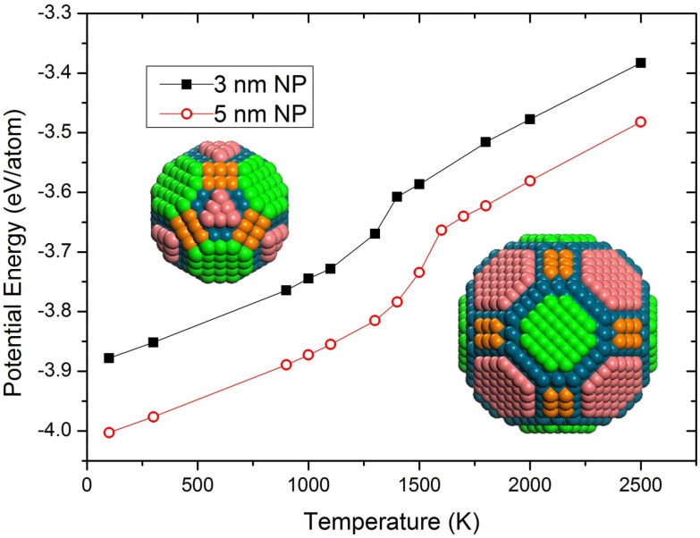
Before conducting any sintering experiments, it is useful to evaluate the melting temperatures of nanoparticles of all sizes of interest. This is readily done in MD by plotting caloric curves for single nanoparticles and determining the points of discontinuity in the potential energy vs. temperature graph (Fig. 1). The jump in the potential energy is a result of the latent heat of fusion released upon melting, and the corresponding temperature is the melting temperature. For palladium nanoparticles with diameters of 3 or 5 nm, melting temperatures of 1400 and 1600 K, respectively, are determined. Some pre-melting can also be observed, since steps become steeper with rising temperature, in agreement with previous studies13,15. The liquid state of a nanoparticle surface is attributed to the contraction of the ionic radii of atoms with reduced coordination number15, a fact computationally confirmed for Pd12. Insets in Fig. 1 show the initial structures for both nanoparticle sizes: green, orange and pink facets correspond to (100), (110) and (111) orientations, respectively. Blue atoms lie beneath the nanoparticle outer surface.
Figure 1. Temperature dependence of potential energy for single palladium nanoparticles 3 and 5 nm in diameter.
Slope changes indicate melting. Insets show initial structures for both nanoparticle sizes: green, orange and pink facets correspond to (100), (110) and (111) orientations, respectively. Blue atoms lie beneath the outer surfaces; however, due to the faceted nature of the nanoparticles, they emerge at edges and vertices.
Coalescence of crystalline nanoparticles
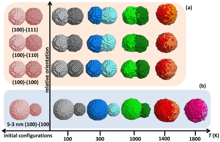
The first effect studied was that of temperature on the coalescence of two identical, perfectly crystalline nanoparticles, 3 nm in diameter. The left-hand side of Fig. 2a depicts the initial configurations of three sets of two nanoparticles oriented in such a way that the (100) facet of the first of each is adjacent to the (100), (110), and (111) facets of the second, respectively. As evident from the final configurations of all relative orientations after 100 ps MD runs (see Fig. 2a, right-hand side, where, for clarity, different colour combinations are assigned to different temperatures), the sintering mechanisms at play depend strongly on temperature. At low temperatures, the two particles just reoriented themselves as rigid objects to form an interface. Coalescence was enhanced at higher temperatures, with necks forming at the interfaces, reaching full fusion at 1400 K, the melting point for Pd nanoparticles of 3 nm diameters. Even at lower temperatures, though, surface pre-melting (assisted by heat released due to free-surface annihilation) enhanced the sintering of the two nanoparticles, and determined the emergent structure.
Figure 2. Parameters affecting nanoparticle coalescence.
(a) Effect of temperature and relative orientation on the coalescence of 2 crystalline Pd nanoparticles, 3 nm in diameter. (b) Effect of temperature and size on the coalescence of 2 crystalline Pd nanoparticles of different sizes (5 and 3 nm in diameter), with touching (100)-type facets. Note that (b) is not to scale with (a). (For clarity, temperatures are represented by shades of colours).
This becomes clearer when size effects are also taken into account. The initial and final configurations after 100 ps MD runs of two crystalline nanoparticles, 5 and 3 nm in diameter, with aligned (100)-type facets are shown in Fig. 2b. At low temperatures, the two particles simply rotated slightly and formed an interface, just like the equal-size cases described above. At 1000 K, the smaller particle was deformed by partial melting and formed a neck almost as thick as its diameter. 1400 K is below the melting point of the 5 nm particle and above that of the 3 nm particle; therefore, the small particle melted completely and wetted the surface of the large one. Here, it might be worth pointing out that, from an engineering point of view, taking advantage of such size-related differences in melting temperatures could potentially be used to design core/shell structures with a uniform shell layer. At 1800 K, both particles were liquid and fully fused together.
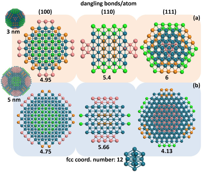
The reason for the initial attraction between the nanoparticles and their subsequent rigid-body rotation is the existence of free bonds on their surfaces. Crystalline Pd has an fcc structure; the coordination number of its bulk atoms is 12. However, due to free surface termination, surface atoms of Pd nanoparticles have lower coordination numbers, leaving the remaining bonds dangling. In Fig. 3, the (100), (110) and (111) facets are tabulated for both nanoparticle sizes. In each case, three layers of atoms are shown, so that all the bonds that the surface atoms form are depicted, as well. Colours correspond to those assigned in the insets of Fig. 1. The average numbers of dangling bonds per atom for each of these facets are shown underneath each facet. These numbers are even larger for atoms lying on edges or vertices of facets. Therefore, they exert forces on nanoparticles that dictate their relative rotation into configurations where surface steps of one nanoparticle match those of the other, thus minimising their free surface area significantly.
Figure 3. Average dangling bond numbers of (100), (110) and (111) facets of both nanoparticle sizes (3 and 5 nm in diameter).
Three layers of atoms are shown, so that all the bonds of the surface atoms are included. To enable all three layers to be visible, atom sizes are smaller for the top row, and increase with depth. Colours correspond to those assigned in Fig. 1. The average numbers of dangling bonds per atom for each of these facets are indicated underneath each facet.
It is interesting to note that the relative misorientation of one nanoparticle with respect to the other brought together facets of different surface areas. It is clear that for the (100)-(100) case (Fig. 2a) the degree of coalescence, indicated by the neck width, was less pronounced than for the other cases, where the two nanoparticles rotated as rigid objects with respect to each other, due to their narrow, asymmetric interfaces. In doing so, they annihilated larger areas of rough free surfaces containing steps, unlike the (100)-(100) case, which resulted in the annihilation of flat free surfaces. To demonstrate the relative motion and coalescence of nanoparticles as clearly as possible, example animations of the (100)-(110) configuration are available in the Supplementary Information online (Supplementary Movies 1–4, corresponding to 100, 300, 1000 and 1400 K, respectively).
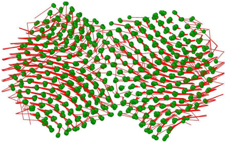
Free surface annihilation led to a reduction of the potential energy of the system, with the resultant heat generation. This heat was sufficient to melt momentarily a region near the interface of the particles. The amount of this melting depended on the initial temperature of the interaction: the closer this initial temperature was to the nanoparticle melting points, the more extensive the melting became. Eventually, this extra heat dissipated through the particles (or was damped, when our choice of statistical ensemble was NVT, see Methods section) and the molten region re-solidified epitaxially to either of the two nanoparticles, which acted as crystallisation seeds. It is at this stage that necks formed, with the atoms of the interface relocating themselves due to the internal stresses they experienced. This relocation is usually accompanied by the formation of misfit dislocations, which slip, creating protrusions on the particle surfaces16. To illustrate the shear stresses that the atoms experience, we drew displacement maps of the atoms during the coalescence process. Such a map depicting atomic displacements for the (100)-(100) configuration at 1000 K is shown in Fig. 4. The atoms are shown at their final positions after a 100 ps MD run, whereas the red lines indicate their original positions at the beginning of the coalescence process, implying their paths. To allow viewing through the bodies of the nanoparticles rather than just the surfaces, depicted atom sizes were reduced, compared to those in Fig. 2. Despite their common initial orientation when they were first brought together, the nanoparticles rotated slightly with respect to each other due to instantaneous asymmetries induced by thermal vibrations. From this figure, it is evident that the ensuing atomic flow in both nanoparticles was dictated by that initial tendency to rotate as rigid objects. The formation of a common neck prevented any further rotation; shear stresses were subsequently introduced, resulting in the protrusions seen on the top of the left-hand side particle and the bottom of the right-hand side one. These protrusions change the original near-spherical shape of the particles dramatically. The serrated shape of the final configuration leads to a potential enhancement of both catalytic and hydrogen adsorption properties, due to increased surface roughness3,9.
Figure 4. Shearing of nanoparticles due to their initial rotation tendency.
Atomic displacement map of 3 nm particles of (100)-(100) relative orientation, after 100 ps MD run of nanoparticle coalescence at 1000 K. Depicted is the final configuration; the initial one is indicated by the start of the red lines. A tendency of the two nanoparticles to rotate against each other is evident. When this was not possible, due to necking, internal stresses developed, which led to the creation of protrusions both sides of the neck.
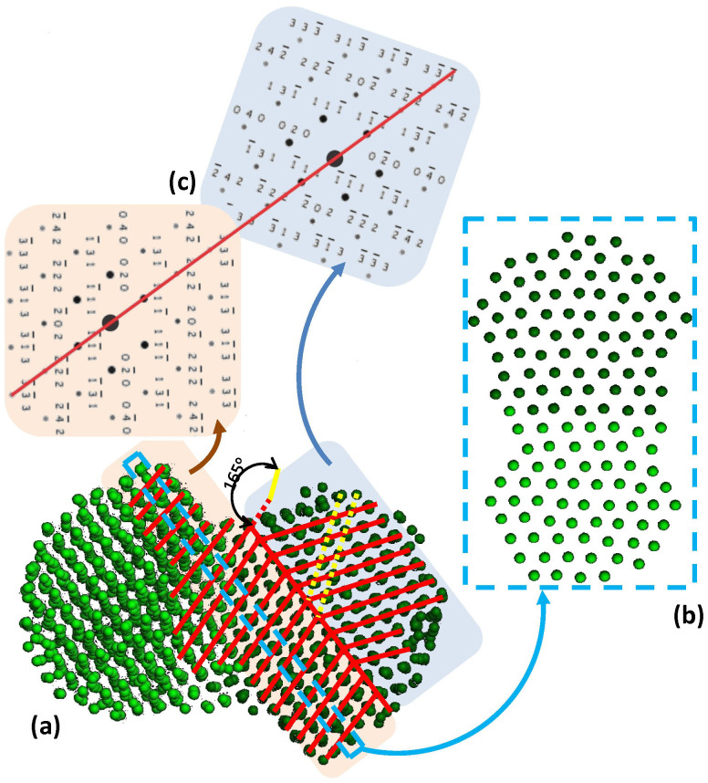
A different view of the (100)-(100) final configuration at 1000 K, shown in Fig. 5, yields another interesting result. Initially the boundary between the two different orientation regions was the interface between the nanoparticles. As mentioned above, a mixed zone was eventually formed at the interface, first through melting and then by epitaxial re-solidification with one or the other particle (in the case depicted in Fig. 5a, the particle on the left). Essentially, mixed zone atoms were not surface atoms any more, and therefore not susceptible to surface pre-melting. This is more clearly illustrated in Fig. 5b, which shows a one-atomic-plane width slab of {111} orientation, cut along the blue dashed rectangle of Fig. 5a. It is obvious that almost perfect epitaxial alignment of atoms both sides of the initial interface was achieved. Thus, the boundary was shifted from the initial interface towards the body of the nanoparticle on the right, forming a twin consisting of two individual crystals joined (at the boundary) in some definite mutual orientation. This is in full agreement with Theissmann et al., who showed that the formation of a twin boundary is the most probable final configuration of sintered particles27.
Figure 5. Formation and shifting of a twin boundary as a result of nanoparticle coalescence.
(a) Final configuration after 100 ps MD run of two nanoparticles coalescing with facing (100)-type facets at 1000 K. Red lines are guides to the eye, for atomic plane orientations. (b) one-atomic-plane width slab of {111} orientation, cut along the blue dashed line of (a). (c) Calculated diffraction patterns of regions both sides of twin boundary.
The lattice of one crystal is related to that of the other by a 70° rotation. Both crystals are presented along the 〈101〉 directions. The corresponding calculated diffraction patterns are shown in Fig. 5c. Diffraction patterns elucidate the direction of the electron beam and the complete orientation of that region of the specimen illuminated by the beam. If the lattice parameter of the crystal is determined, one can calculate the allowed reflections and the specific d-spacings which are associated with diffraction spots (reflections)28. Once possible values for the magnitude of the g vectors (g = 1/d-spacing) for the identified reflections have been tentatively identified, the results can be cross-checked using the angles between the g vectors (i.e., the angles between the plane normals). Finally, the consistency of this indexing can be verified using the Weiss zone law. Each hkl reflection must lie in the [UVW] zone axis of the diffraction pattern, i.e., hU + kV + lW = 0.
It is evident that the boundary plane is of the {111} type, and that the stacking sequence of the {111} planes on the one side of the twin interface is a mirror image of the stacking sequence of those on the other side. To clarify the twinned structure, in Fig. 5a, the {111} planes of both domains, as well as the interface, are denoted by red lines. The boundary plane is also indicated by a red line on the corresponding calculated diffraction pattern. It should be noted that the {111} planes of the twin-related domains exhibit an angle of ~140°, while the {111} planes of the left domain exhibit an angle equal to ~165° with the {020} planes (denoted by yellow dashed lines) of the right domain. Those angles, too, can be readily confirmed on the corresponding calculated diffraction patterns; it is well known that the angle between two {111} planes in a Pd crystal structure is 70.529°, while that between {111} planes and {020} planes is either 54.736° or 125.264°.
To confirm this mechanism experimentally by comparison to our simulation results, we grew Pd nanoparticle porous films, using a technique recently reported by Singh et al.10,18 that utilises a Mantis Deposition Ltd synthesis reactor, with DC magnetron sputtering, gas-aggregation, and mass filtration, to create a size-selected nanocluster beam (see Methods section). A similar method was used by Ayesh et al. to grow Pd nanoclusters6. An example of an HRTEM image of a resultant, as-deposited, Pd nanoparticle film is shown in Fig. 6. Two nanoparticles are observed along the 〈101〉 direction, with the {111} planes and the corresponding d-spacings indicated. The left nanoparticle is captured edge-on the 〈101〉 direction and the bounding facets ({111} in yellow dashed lines, and {020} in red) are depicted. In contrast, the right nanoparticle is slightly off-axis and the {111} planes are found to be rotated with respect to the left nanoparticle. In addition, a third, smaller nanoparticle is visible, in which the {220} planes are identified. It is noteworthy that, just like the examples in this figure, the vast majority of all the deposited nanoparticles which were identified through HRTEM exhibit crystallinity.
Figure 6. HRTEM image of a Pd nanoparticle film.
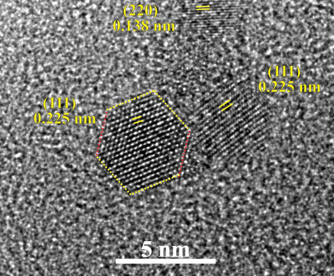
Three Pd nanoparticles are shown, and specific planes and spacings are indicated. The larger one on the right has a diameter of about 5 nm while the smallest one at the top of the image has a diameter of about 3 nm.
In the HRTEM image of Fig. 7, starting from the lower right-hand side, a Pd nanoparticle projected along the 〈001〉 direction is identified. The crystal structure is well defined, and the {220} planes and the corresponding d-spacing are denoted on the image, just as in Fig. 6. Next to the aforementioned nanoparticle, another domain is observed edge-on along the 〈101〉 direction, where the {111} planes are visible as given. There exists a third domain in the upper left-hand side of the figure, with its {200} planes identified. Remarkably, the latter two domains exhibit the exact twin structure that emerged in our MD simulations from the coalescence of two nanoparticles with (100)-type facets. The angle between these {200} planes and the {111} planes of the central domain is equal to ~165°, the angle that characterises the twin boundary described in Fig. 5a. The twin boundary plane, which lies along a set of common {111} planes belonging to both of the two neighbouring domains, is denoted by a yellow dashed line. Therefore, it would not be unreasonable to assume that coalescence of the two nanoparticles may have led to the formation of the twin, through a mechanism similar to the one describing our simulation results.
Figure 7. HRTEM image of coalesced Pd nanoparticles.
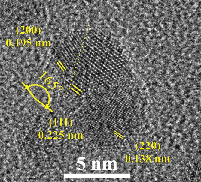
The two nanoparticles exhibiting the (111) and (200) planes form the twin structure which emerged in our MD simulations, presented in Fig. 5a. The twin boundary is denoted by a yellow dashed line (see text for details).
Coalescence of amorphous nanoparticles
Finally, the sintering of two amorphous nanoparticles 3 nm in diameter was studied, as depicted in Fig. 8a. At low temperatures the particles partly sinter with each other forming necks, whereas at higher temperatures full coalescence occurs. It is noteworthy that the degree of partial coalescence at low temperatures is more pronounced than in any of the crystalline cases mentioned above, due to the easier surface pre-melting of amorphous clusters. Most importantly though, one can notice the emergence of ordered facets at all solid final configurations, implying that crystallisation of the two-nanoparticle system took place as a side-effect of partial coalescence. Examples of such facets are denoted on the 300 and 1000 K configurations of Fig. 8a.
Figure 8. Coalescence-induced crystallisation of amorphous Pd nanoparticles.
(a) Final configurations after 100 ps MD run of two amorphous nanoparticles coalescing at various temperatures. Emerging facets of specific crystallographic planes are denoted for the 300 and 1000 K configurations, which are enlarged at (b) and (c), respectively. Epitaxial atomic arrangement and formation of twinned crystallites is clear in both cases. (For clarity, temperatures are represented by shades of colours).
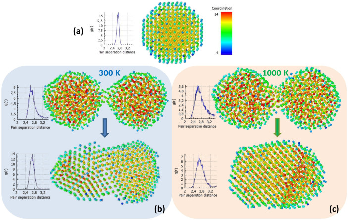
This is more clearly illustrated in Figs. 8b and c, where the final configurations at 300 and 1000 K are depicted, once again with reduced atomic size so that a view through the bodies of the particles is possible. In both cases it is evident that coalescence-induced crystallisation occurred. In the 300 K case (Fig. 8b), corresponding to nanoparticle coalescence at room-temperature on the substrate, multiple grains were formed, whereas in the 1000 K case (Fig. 8c), corresponding to in-flight collisions of hot, newly-formed clusters, almost full epitaxial crystallisation was achieved, assisted by the higher temperature.
A more elaborate quantitative study of this phenomenon is presented in Fig. 9, where atomic coordination colour maps of the aforementioned configurations are shown. As a reference, in Fig. 9a a map of a perfectly crystalline nanoparticle at a low temperature (100 K) is illustrated. Practically all the atoms, save for the surface ones, are illustrated in yellow, which corresponds to a coordination number of 12, the coordination number of atoms in fcc crystals. As mentioned in the previous sub-section, surface atoms have a lower coordination number; they are depicted in light or dark blue in the map, depending on whether they are located on an edge or a vertex. The atomic radial distribution function29 of the nanoparticle is also shown. The distribution has a narrow peak around the value of 2.7 Å, which is the nearest-neighbour distance for Pd crystals. Changes of atomic coordination between the initial and final configurations of Fig. 8 at 300 and 1000 K are shown in Figs. 9b and c, respectively. At both temperatures, changes from multi-coloured mixtures in the initial frames to practically all-yellow configurations in the final ones are observed. Narrowing of the radial distribution function peaks around the crystalline value (2.7 Å) also indicate extended crystallisation. This tendency appears less pronounced at 1000 K, but that is due to atomic thermal vibrations, which lead to deviations from the theoretical nearest-neighbour distance.
Figure 9. Atomic coordination colour maps for various configurations.
(a) Perfectly crystalline Pd nanoparticle, 3 nm in diameter, at 100 K, as reference. Yellow atoms exhibit the fcc coordination number of 12, also evident by the radial distribution function showing a peak at 2.7 Å. Lower coordination surface atoms appear blue. Changes of atomic coordination after 100 ps MD runs of nanoparticle coalescence at 300 and 1000 K are shown in (b) and (c), respectively. Both colour changes and narrowing of radial distribution function peaks around the crystalline value (2.7 Å) indicate extended crystallisation.
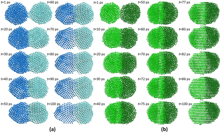
Animations presenting the evolution of the systems are available in the Supplementary Information online (Supplementary Movies 5 and 6, corresponding to 300 and 1000 K, respectively), and clearly show that crystallisation starts at the interface, due to the high stresses present, and gradually advances away from it. More specifically, these stresses accumulate until they are finally released by a rigid-body rotation of one particle (in our cases, the ones on the right). This rotation triggers a crystallisation wave propagating through the body of the other particle. This is in complete agreement with the in-situ TEM observations of José-Yacamán et al., who noted the separate rotations of Pd nanoparticles and their plane alignment to form new particles with a unique fcc structure15. Frequent snapshots from our animations are shown in Figs. 10a and b for 300 and 1000 K, respectively, illustrating the mechanism described above. Therefore, for amorphous Pd nanoparticles to crystallise, the presence of existing crystal seeds is not a prerequisite.
Figure 10. Evolution of coalescence of two Pd nanoparticles, at varying time intervals.
(a) 300 K and (b) 1000 K. A crystallisation wave, propagating from right to left is evident at both temperatures, leading to a polycrystalline (a) or an almost mono-crystalline (b) structure. In both cases, the wave was initiated by a rigid-body rotation of the nanoparticle on the right.
To summarise, Pd nanoparticles find many industrial applications, predominantly ones related to its catalytic efficiency and hydrogen adsorption capacity. Given the correlation between these properties and surface geometry, nanoparticle coalescence studies can shed light on the mechanisms that govern the structures formed and provide insight into growth parameters in order to optimise performance.
With this study we obtained a detailed qualitative understanding of these mechanisms and an evaluation of parameters that affect them. The driving force for coalescence was confirmed to be surface energy minimisation, associated with dangling bond density and distribution. Initial nanoparticle reorientation was followed by the creation of an interface and necking at low temperatures, or full consolidation at higher ones. In the case of crystalline nanoparticles, twin boundaries, which originally formed at the original nanoparticle interface, moved randomly towards their interior, accompanied by the formation of protrusions. Both are associated with atomic reorganisation into a, more-or-less, epitaxial orientation. In doing so, the intrinsic stresses introduced to the system through the initial nanoparticle rigid-body rotations were minimised. The rough surfaces, mainly formed at, or near, the necks between the sintered particles, are believed to be beneficial to catalytic and hydrogen adsorbing properties.
More importantly, coalescence-assisted crystallisation was observed during sintering of amorphous nanoparticles. Extensive neck formation temporarily pinned down the rotation of the nanoparticles, introducing stresses in their interface. When the particles eventually managed to break free, their additional rotation initiated a seedless crystallisation wave, which propagated through them, leading to near-perfect single- or polycrystalline fcc structures.
Methods
Molecular dynamics simulations
For this study, we used the Accelrys© Materials Studio Suite, and more specifically the GULP parallel, classical MD code30. We created Pd nanoparticles 3 and 5 nm in diameter, either crystalline (space group 225:  , lattice constant 3.89 Å) or amorphous, containing 976 and 4,508 atoms, respectively. The crystalline ones obtained TO structures, with the 5 nm ones forming perfectly symmetrical octahedra with square and regular-hexagon facets, and the 3 nm ones forming a shape in-between a TO and a cuboctahedron, a special TO with square and triangular facets. Both structures are shown in the insets of Fig. 1.
For the interatomic forcefield, we opted for the embedded-atom method Johnson potential31 for fcc metals. It was originally fitted on such physical input as equilibrium lattice constant, cohesive energy etc., and has been used to describe both Pd alloys32 and metallic fcc nanoparticle properties33. We used both the canonical NVT and micro-canonical NVE ensembles with the rationale that the former resembles better a situation where the nanoparticles are thermally coupled to a substrate which acts as a heat sink at a certain temperature, and the latter simulates better in-flight nanoparticle coalescence under vacuum18. Since we got qualitatively similar results for both, in our report no specific mention of a statistical ensemble was made. We initially optimised geometrically each of our nanoparticles alone by Molecular Statics (MS) runs, using the Newton-Raphson optimiser and the BFGS method34. Then, we equilibrated them separately for up to 30 ps at all temperatures within the temperature range we wanted to study, namely 100, 300, 1000, 1400, and 1800 K. We subsequently created a number of different configurations bringing together 2 nanoparticles at distances within the interatomic potential range and performed MD runs on them for 100 ps, using time-steps of 1–3 fs. Our choice of simulation time was based on previous literature reports16, but was also dictated by practical restrictions. Monitoring the evolution of our systems, we confirmed that they presented all interesting behaviour and reached stable configurations within ~75% of the simulation time.
Atomic displacement and coordination number maps, as well as radial distribution functions were analysed using Ovito 235.
Nanoparticle deposition
Pd nanoparticles were deposited using a gas-aggregated sputtering system from Mantis Deposition Ltd (Oxon, UK). The gas-aggregated sputtering technique was originally reported by Haberland et al.36. The interested reader is referred to cited studies37,38,39 for exemplary recent works. Pd was sputtered using an Ar plasma, from a 25 mm diameter source target. An initial high-pressure aggregation zone was formed by restricting the pumping of the region via a 5 mm aperture, and water-cooling the chamber sidewalls at 16°C. The large pressure differential causes the particles to be accelerated from the (high-pressure) aggregation zone into the lower pressure region on the other side of the aperture. The nanoparticles then pass through a mass filter, and finally enter the deposition chamber to land on the substrate. For TEM studies, the substrate was a copper frame grid covered with a thin (<20 nm) membrane of amorphous carbon.
Transmission electron microscopy analysis
TEM studies were carried out using a 300 kV FEI Titan microscope, equipped with a post-specimen spherical aberration corrector for bright field TEM imaging. In image-corrected TEM mode, the spherical and chromatic aberrations were <5 μm and 1.4 mm, respectively, with an optimum resolution of better than 0.09 nm. In STEM mode, the spherical and chromatic aberrations were 1.2 mm and 1.4 mm, respectively, with optimum HAADF−STEM resolution of better than 0.136 nm. Energy dispersive x-ray spectroscopy (EDS) was performed with an Oxford X−max system, with an 80 mm2 silicon drift detector (SDD) and energy resolution of 136 eV.
Author Contributions
P.G. carried out the MD computer simulations, performed the analysis of their results, and wrote the manuscript. V.S. deposited the nanoparticles. C.C. performed the TEM imaging. M.S. conceived the idea, designed the experimental work and led the project. All authors reviewed the manuscript.
Supplementary Material
Supplementary Information
Summplementary Movie 1
Supplementary Movie 2
Supplementary Movie 3
Supplementary Movie 4
Supplementary Movie 5
Supplementary Movie 6
Acknowledgments
The authors would like to gratefully acknowledge the contribution of Dr Abhijit Chatterjee for his valuable technical advice, and Mr Antony D. Galea for proofreading and editing the manuscript.
References
- El Far R. et al. Quantitative determination of hydrogen absorption by Pd cluster-assembled films using a quartz crystal microbalance. Thin Solid Films 522, 199–203 (2012). [Google Scholar]
- Cookson J. The preparation of palladium nanoparticles. Platinum Metals Rev. 56, 83–98 (2012). [Google Scholar]
- Mohanty A., Garg N. & Jin R. A universal approach to the synthesis of noble metal nanodentrites and their catalytic properties. Angew. Chem. Int. Ed. 49, 4962–4966 (2010). [DOI] [PubMed] [Google Scholar]
- Fan Y. et al. Nanoparticle decorated anodes for enhanced current generation in microbial electrochemical cells. Biosens. Bioelectron. 26, 1908–1912 (2011). [DOI] [PubMed] [Google Scholar]
- Nobelprize.org., The Nobel Prize in Chemistry 2010 - Advanced Information (2013) 25/12/2013. <http://www.nobelprize.org/nobel_prizes/chemistry/laureates/2010/advanced.html>.
- Ayesh A. I., Thaker S., Qamhieh N. & Ghamlouche H. Size-controlled Pd nanoclusters grown by plasma gas-condensation method. J. Nanopart. Res. 13, 1125–1131 (2011). [Google Scholar]
- Tsantilis S., Pratsinis S. E. & Haas V. Simulation of synthesis of palladium nanoparticles in a jet aerosol flow condenser. J. Aerosol Sci. 30, 785–803 (1999). [Google Scholar]
- Ayesh A. I. Electronic transport in Pd nanocluster devices. Appl. Phys. Lett. 98, 133108 (2011). [Google Scholar]
- Han J., Hu W. & Deng H. Adsorption of hydrogen on palladium nanoparticle surfaces. Surf. Interface Anal. 41, 590–594 (2009). [Google Scholar]
- Singh V. et al. Surface morphology of films grown by size-selected Ta nanoparticles. Adv. Mat. Res. 647, 732–737 (2013). [Google Scholar]
- Kasper N. et al. In situ oxidation study of MgO(100) supported Pd nanoparticles. Surface Science 600, 2860–2867 (2006). [Google Scholar]
- Qi W., Huang B. & Wang M. Structure of unsupported small palladium nanoparticles. Nanoscale Res. Lett. 4, 269–273 (2009). [DOI] [PMC free article] [PubMed] [Google Scholar]
- Ling M., Venkat R. B. & Babu J. Melting of Pd clusters and nanowires: a comparison study using molecular dynamics simulation. Phys. Rev. B 72, 134109 (2005). [Google Scholar]
- Schebarchov D. & Hendy S. C. Solid-liquid phase coexistence and structural transitions in palladium clusters. Phys. Rev. B 73, 121402(R) (2006). [DOI] [PubMed] [Google Scholar]
- José-Yacamán et al. Surface diffusion and coalescence of mobile metal nanoparticles. J. Phys. Chem. B 109, 9703–9711 (2005). [DOI] [PubMed] [Google Scholar]
- Zhu H. & Averback R. S. Sintering processes of two nanoparticles: a study by molecular dynamics simulations. Phil. Mag. Lett. 73, 27–33 (1996). [Google Scholar]
- Eggersdorfer M. L., Kadau D., Herrmann H. J. & Pratsinis S. E. Aggregate morphology evolution by sintering: number and diameter of primary particles. J. Aerosol Sci. 46, 7–19 (2012). [DOI] [PMC free article] [PubMed] [Google Scholar]
- Grammatikopoulos P., Cassidy C., Singh V., Benelmekki M. & Sowwan M. Coalescence behaviour of amorphous and crystalline tantalum nanoparticles: a molecular dynamics study. J. Mater. Sci. 49, 3890–3897 (2014). [Google Scholar]
- Arcidiacono S., Bieri N. R., Poulikakos D. & Grigoropoulos C. P. On the coalescence of gold nanoparticles. Int. J. Multiphas. Flow 30, 979–994 (2004). [Google Scholar]
- Zhao S. J., Wang S. Q. & Ye H. Q. Coalescence of three silver nanoclusters: a molecular dynamics study. J. Phys. Condens. Matter 13, 8061–8069 (2001). [Google Scholar]
- Kart H. H., Wang G., Karaman I. & Çağin T. Molecular dynamics study of the coalescence of equal and unequal sized Cu nanoparticles. Int. J. Mod. Phys. C 2, 179–196 (2009). [Google Scholar]
- Lewis L. J., Jensen P. & Barrat J. L. Melting, freezing, and coalescence of gold nanoclusters. Phys. Rev. B 56, 2248–2257 (1997). [Google Scholar]
- Ding F., Rosén A. & Bolton K. Size dependence of the coalescence and melting of iron clusters: a molecular dynamics study. Phys. Rev. B 70, 075416 (2004). [Google Scholar]
- Ogata S. et al. Role of atomic charge transfer on sintering of TiO2 nanoparticles: variable-charge molecular dynamics. J. Appl. Phys. 88, 6011 (2000). [Google Scholar]
- Chatterjee A. et al. Sintering, structure and mechanical properties of nanophase SiC: A molecular-dynamics and neutron scattering study. Appl. Phys. Lett. 77, 1132 (2000). [Google Scholar]
- Campbell T. et al. Structural correlations and mechanical behaviour in nanophase silica glasses. Phys. Rev. Lett. 82, 4018 (1999). [Google Scholar]
- Theismann R. et al. Crystallographic reorientation and nanoparticle coalescence. Phys. Rev. B 78, 205413 (2008). [Google Scholar]
- Williams D. B. & Carter C. B. [Chapter 18: Obtaining and indexing parallel-beam diffraction patterns]. Transmission Electron Microscopy: A Textbook for Materials Science [287–290] (Springer, New York, 2009). [Google Scholar]
- Hansen J.-P. & McDonald I. R. [Chapter 2: Statistical mechanics]. Theory of simple liquids [29–30] (Academic Press, Waltham, 2006). [Google Scholar]
- Gale J. D. GULP: a computer program for the symmetry-adapted simulation of solids. J. Chem. Soc. Faraday Trans. 93, 629–637 (1997). [Google Scholar]
- Johnson R. A. Alloy models with the embedded-atom method. Phys. Rev. B 39, 12554 (1989). [DOI] [PubMed] [Google Scholar]
- Mousseau N. & Thorpe M. F. Length distributions in metallic alloys. Phys. Rev. B 45, 2015 (1992). [DOI] [PubMed] [Google Scholar]
- Gracia-Pinilla M. Á. et al. On the structure and properties of Silver Nanoparticles. J. Phys. Chem. C 112, 13492 (2008). [Google Scholar]
- Leach A. R. [Chapter 5: Energy minimisation and related methods for exploring the energy surface]. Molecular Modelling: Principles and Applications [267–270] (Pearson Education Limited, Essex, 2001). [Google Scholar]
- Stukowski A. Visualization and analysis of atomistic simulation data with OVITO – the Open Visualization Tool. Modelling Simul. Mater. Sci. Eng. 18, 015012 (2010). [Google Scholar]
- Haberland H. et al. Filling of micron-sized contact holes with copper by energetic cluster impact. J. Vac. Sci. Technol. A. 12, 2925 (1994). [Google Scholar]
- Straňák V. et al. Size-controlled formation of Cu nanoclusters in pulsed magnetron sputtering system. Surf. Coat. Tech. 205, 2755–2762 (2011). [Google Scholar]
- Gracia-Pinilla M. Á., Martínez E., Vidaurri G. & Pérez-Tijerina E. Deposition of size-selected Cu nanoparticles by inert gas condensation. Nanoscale Res. Lett. 5, 180–188 (2010). [DOI] [PMC free article] [PubMed] [Google Scholar]
- Nielsen R. M. et al. The morphology of mass selected ruthenium nanoparticles from a magnetron-sputter gas-aggregation source. J. Nanopart. Res. 12, 1249–1262 (2010). [Google Scholar]
Associated Data
This section collects any data citations, data availability statements, or supplementary materials included in this article.
Supplementary Materials
Supplementary Information
Summplementary Movie 1
Supplementary Movie 2
Supplementary Movie 3
Supplementary Movie 4
Supplementary Movie 5
Supplementary Movie 6


