Abstract
A major technical hurdle in microfluidics is the difficulty in achieving high fidelity lithographic patterning on polydimethylsiloxane (PDMS). Here, we report a simple yet highly precise and repeatable PDMS surface micromachining method using direct photolithography followed by reactive ion etching (RIE). Our method to achieve surface patterning of PDMS applied an O2 plasma treatment to PDMS to activate its surface to overcome the challenge of poor photoresist adhesion on PDMS for photolithography. Our photolithographic PDMS surface micromachining technique is compatible with conventional soft lithography techniques and other silicon-based surface and bulk micromachining methods. To illustrate the general application of our method, we demonstrated fabrications of large microfiltration membranes and free-standing beam structures in PDMS.
Introduction
Polydimethylsiloxane (PDMS) is one of the most frequently used structural materials in microfluidics, due to its great biocompatibility, optical transparency, gas permeability, mechanical elasticity, and electrical insulation.1–2 The complexity of PDMS-based microfluidic systems is also increasing rapidly as sophisticated functions have being integrated into single microfluidic devices.3 Just as the surface patterning techniques using lithography and etching processes have been the major drivers for the successful development of micro-electro-mechanical systems (MEMS), there is an increasing demand in the field of microfluidics for highly reliable, repeatable and precise surface micromachining techniques to pattern PDMS for different practical microfluidic and bioengineering applications.
However, till now, PDMS has been largely considered incompatible with conventional lithography, due to its low surface energy resulting in dewetting of photoresist on the PDMS surface.4 Soft lithography is a popular micromachining technique for rapid fabrication of PDMS structures.1–2 Yet, soft lithography is a bulk micromachining technique, and it largely relies on replica molding, which often leaves behind a thin residual PDMS layer on top of the mold features. Through holes in bulk PDMS are typically achieved by punching through the PDMS structures, which can only generate macroscopic openings in PDMS and is far from a precise patterning method. High fidelity PDMS surface micromachining so far remains a major technical hurdle for the microfluidics research.
Several approaches for surface patterning of PDMS have been reported recently, even though each of these methods has its intrinsic constraints that have limited the scopes of their applications in microfluidics. Ryu et al. have reported a simple PDMS patterning method by mechanically removing excessive PDMS prepolymer from a pre-patterned mold using a traversing blade.4 However, this mechanical scrapping method could limit the achievable minimum PDMS film thickness and its pattern resolution and uniformity. Another example is the photo-patternable silicone introduced by Dow Corning.5–6 This photosensitive silicone can be conveniently patterned as traditional negative photoresists. However, it also suffers with the drawbacks associated with negative photoresists in terms of their high cost and limited resolution. Bhagat et al. and some others have proposed another photo-patterning approach by addition of photoinitiators such as benzophenone or 2,2-dimethoxy-2-phenyl acetophenone (DMAP) into PDMS prepolymer to make it photosensitive and thus directly photo-patternable.7–8 Yet, during UV exposure, the photomasks need to be kept at a minimum distance (~80 µm) from the PDMS prepolymer to avoid their direct contact. Thus, pattern resolution achieved using these photosensitive PDMS was significantly limited as compared to conventional photolithography operated in the contact mode. The cytotoxic effects of benzophenone or DMAP have not been well characterized yet and thus could present potential problems for biological applications. More recently, a rapid prototyping technique using direct UV-lithography followed by chemical development for pre-cured PDMS was introduced by Scharnweber et al.9 Although this technique does not introduce undesirable chemical components into PDMS, its pattern resolution is still limited by the required chemical development.
Researchers have also recently attempted using intermediary adhesion layers, such as metal or polydimethyl-glutarimide (PMGI), to permit high-resolution lithography on PDMS.10–11 Still, these methods unavoidably require complex processing steps, and undesirable alterations of the surface and mechanical properties of PDMS could be introduced. For example, the spontaneous buckling of the metal film could result in a permanent deformation of PDMS during thermal curing.12
In this technical note, we present an easily-implementable wafer-level surface micromachining method to generate different planar PDMS microstructures using direct photolithography followed by reactive-ion etching (RIE). Our technique does not induce undesired chemical components into PDMS and can be conveniently integrated with conventional silicon (Si)-based surface and bulk micromachining techniques and other PDMS-based soft lithography methods. Our PDMS surface micromachining technique permits high fidelity lithographic patterning of PDMS structures with a resolution comparable to conventional photolithography (~2 µm). As a proof of its general applicability, we have applied this PDMS surface micromachining technique to generate different planar PDMS microstructures, such as patterned PDMS microfiltration membranes and free-standing beam structures, with their thickness ranging from sub-microns to tens of microns.
Fabrication methods
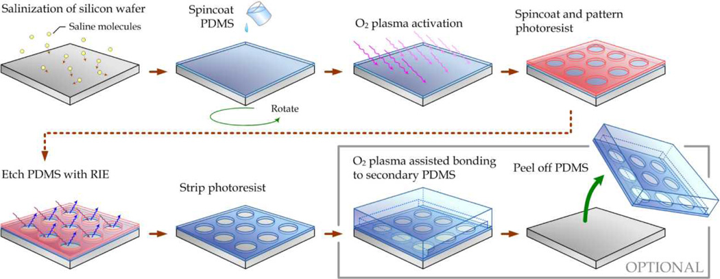
The fabrication process for surface micromachining of PDMS is illustrated in Fig. 1. A Si wafer was first silanized with (tridecafluoro-1,1,2,2,-tetrahydrooctyl)-1-trichlorosilane (United Chemical Technologies, Bristol, PA) for 1 hr under vacuum to facilitate subsequent release of patterned PDMS layers. PDMS prepolymer (Sylgard-184, Dow Corning, Midland, MI) was prepared by thoroughly mixing the PDMS curing agent with the PDMS base monomer (wt:wt=1:10). PDMS prepolymer was then spin coated on the silanized Si wafer and completely cured at 110°C for 4 hrs. The thickness of the PDMS layer, ranging from hundreds of microns down to ~2 µm, could be controlled easily by the spin speed. To achieve ultra-thin PDMS layers with a sub-micron thickness, the PDMS prepolymer could be further diluted with hexane (Fisher Scientific, Pittsburgh, PA) to reduce its viscosity.13 It has been reported that this strategy could generate PDMS layers with a thickness as thin as ~70 nm.13 In this work, with a weight ratio of PDMS curing agent:base:hexane as 1:10:20, PDMS thin films with a thickness of 500 nm were achieved by spin coating the diluted PDMS prepolymer at 5,000 rpm for 2 min. A surface profilometer (Dektak 6M surface profiler, Veeco Instruments, Plainview, NY) was then used to measure thickness of the PDMS layer.
Fig. 1.
Schematic of photolithographic surface micromachining of PDMS.
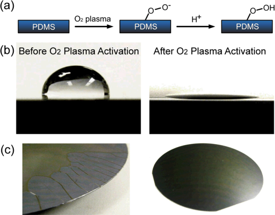
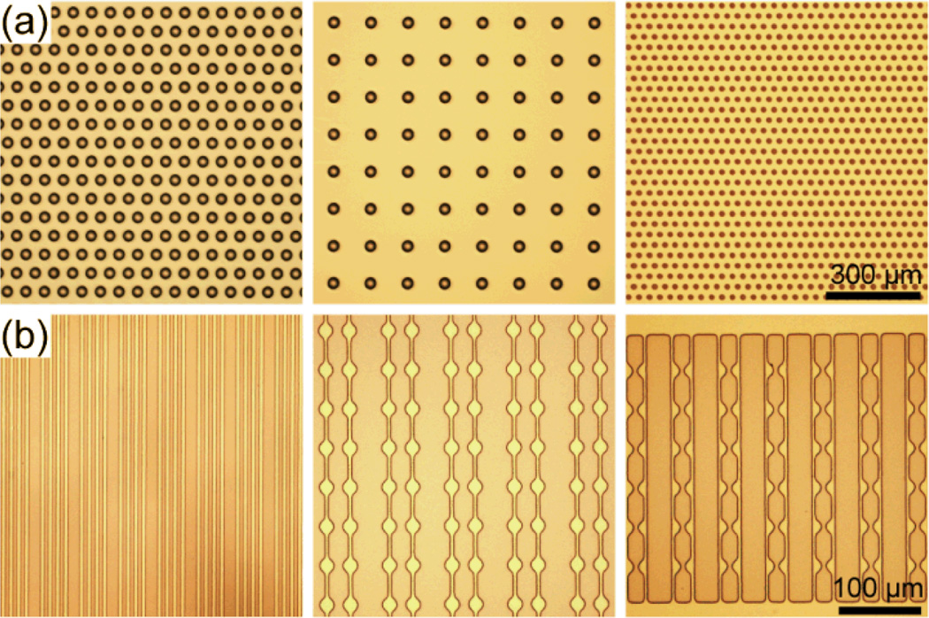
The PDMS surface was then activated using a gentle treatment of O2 plasma (Plasma Cleaner PDC-001, Harrick Plasma, Ithaca, NY) for 5 min to change the PDMS surface from hydrophobic to hydrophilic, in order to allow uniform coating of photoresist in the following step (Fig. 2; enlarged images see Supplemental Fig. S1). Immediately following the O2 plasma activation, photoresist such as AZ 9260 (AZ Electronic Materials, Branchburg, NJ) or SPR 220 (Rohm and Haas, Philadelphia, PA) was spin-coated uniformly on PDMS, soft baked at 110°C for 3 min, and then patterned using conventional contact or projection photolithography. It should be noted that sudden temperature changes should be avoided after soft bake of photoresist, as cracks in the photoresist layer might develop owning to the known issue of a mismatch of the coefficient of thermal expansion (CTE) between PDMS and photoresist. The Si wafer was then processed with RIE (LAM 9400, Lam Research, Fremont, CA) using SF6 and O2 gas mixtures to transfer patterns from the photoresist to the underlying PDMS layer. During the RIE process, the reactive gas ions would etch anisotropically the exposed PDMS regions where the photoresist had been previously developed and dissolved. (Details of the RIE process are discussed in the next section.) Photoresist was then striped using solvents or O2 plasma, leaving patterned PDMS thin films attaching on the Si wafer (Fig. 3; enlarged images see Supplemental Fig. S2).
Fig. 2.
Effect of O2 plasma treatment on coating photoresist on Si wafer. (a) Surface hydrophilization of PDMS using O2 plasma treatment. (b) Contact angles of water drops on PDMS before (100°, left) and after (<5°, right) 5 min treatment of O2 plasma. (c) Images of photoresist layer spin-coated on PDMS surface with (right) and without (left) treatment O2 plasma. Photoresist could not be spread out uniformly on the PDMS surface without O2 plasma treatment (left), while after O2 plasma treatment, the photoresist could be uniformly spin-coated on PDMS.
Fig. 3.
Bright-field images of patterned PDMS layers on Si wafers. (a) Arrays of through holes with the hole diameters of 20 µm (left and middle) and 8 µm (right). (b) PDMS strips of different line widths.
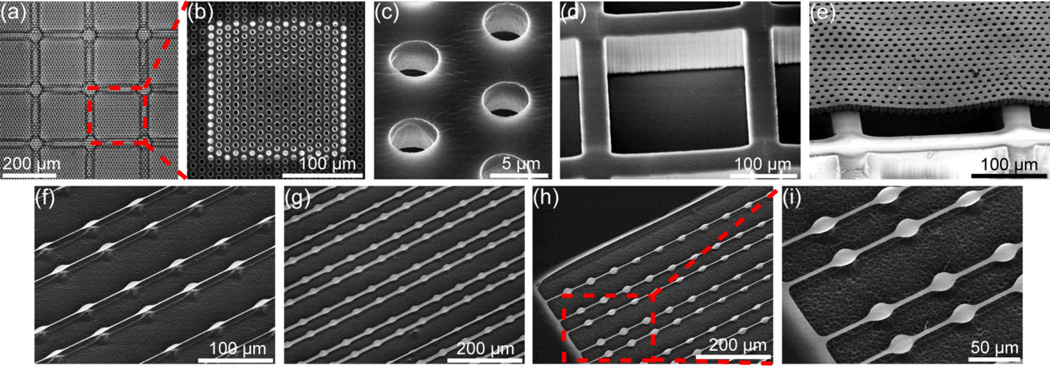
Our photolithographic method for surface micromachining of PDMS could be easily integrated with other conventional microfabrication techniques to generate functional microfluidic devices for different biomedical applications. As shown in Fig. 3a & Fig. 4a–e, large PDMS microfiltration membranes with arrays of through holes of different diameters were generated using our photolithographic PDMS surface micromachining method. These PDMS microfiltration membranes had a thickness of 2–20 µm, and they contained hexagonally spaced or square arrays of through holes with the hole diameter and center-to-center (c.t.c.) distance precisely defined by photolithography (the hole diameter of 4–20 µm and c.t.c. distance of 6–200 µm). Using the O2 plasma-assisted PDMS bonding process, the PDMS microfiltration membrane was further transferred onto a secondary bulk PDMS, whose surface contained square-shaped support microstructures fabricated using soft lithography, to provide a superior mechanical strength for the large microfiltration membrane. As another example, free-standing thin PDMS beam structures (with a thickness of 500 nm) were successfully fabricated using XeF2-based bulk Si dry etching (Xetch X4 series, XACTIX, Pittsburgh, PA) after surface pattering of PDMS on the Si wafer (Fig. 3b and Fig. 4f–i). Using contact photolithography, the minimum beam width along these free-standing PDMS beam structures was as small as 2 µm.
Fig. 4.
Photolithographic surface micromachining of free-standing PDMS microfiltration membranes and beam structures. (a–e) Bright-field (a) and SEM (b–e) images of a PDMS microfiltration membrane, bonded to a PDMS support structure (d). The microfiltration membrane had a thickness of 10 µm and it contained an array of hexagonally spaced through holes (with a hole diameter of 4 µm). (f–i) Free-standing PDMS beam structures on Si wafers, with the beam thickness of 500 nm and total beam length of 800 µm. The minimum beam width were 2 µm (f), 10 µm (g), 5 µm (h & i), respectively.
Process discussion
In this work, we used a simple O2 plasma treatment to address the major technical hurdle for wafer-level surface machining of PDMS: dewetting of photoresist on the intrinsically hydrophobic PDMS surface. The difficulty in spin coating photoresist directly onto the untreated PDMS surface is because of its low surface energy (~23 mN m−1), which is originated from the shielding effect of the nonpolar methyl groups (carbon and hydrogen containing groups) on the polar siloxane backbone, resulting in a tendency for photoresist to dewet on PDMS.11, 15 We showed that a brief treatment of O2 plasma for the PDMS surface could create super-hydrophilicity on the PDMS surface, by stripping methyl groups from the PDMS surface which could then form silanols1, 11, 16 (Fig. 2a). As evidence of this super-hydrophilicity on the PDMS surface after the O2 plasma treatment, the contact angle of a water droplet was dramatically reduced from about 100° (on untreated PDMS; Fig. 2b, left) to <5° (on plasma-treated PDMS; Fig. 2b, right). After the O2 plasma activation of PDMS, a uniform photoresist layer could be successfully spin-coated onto the PDMS surface (Fig. 2c, right; enlarged images see Supplemental Fig. S1), which could be difficult to achieve for the untreated PDMS surface (Fig. 2c, left). It should be noted that the effect of O2 plasma treatment was not permanent and would decay within a few hours as the low molecular weight siloxane chain in the bulk PDMS could migrate to its surface.11, 17 Hence, the O2 plasma treatment of the PDMS surface could temporarily establish a hydrophilic surface suitable for spin coating photoresist uniformly, and this O2 plasma treatment will not introduce permanent alterations of the PDMS surface property.
We further optimized the RIE process for anisotropic dry etching of PDMS using SF6 and O2 gas mixtures and achieved a maximum PDMS etch rate of ~0.8 µm/min with a vertical etch profile and a smooth etched surface. As shown in Fig. 4, different planar PDMS structures (i.e. large PDMS microfiltration membranes and free-standing thin PDMS beam structures) with a thickness ranging from submicron up to tens of microns were fabricated using RIE-based dry etching of PDMS. After 15-min etching of PDMS, the root-mean-square (RMS) surface roughness of the etched PDMS surface measured by atomic force microscopy (AFM, Digital Instruments, Tonawanda, NY) was about 1 nm, comparable to the intrinsic surface roughness of unprocessed PDMS (data not shown). It has been reported that reactive plasma generated using CF4 and O2 gases could also etch PDMS, yet we observed that RIE process using such gases could result in a large surface roughness (~µm) for the etched PDMS surface (data not shown).18 To further examine the anisotropic etch profile for PDMS after the RIE process using SF6 and O2 gas mixtures, cross-sectional scanning electron microscopy (SEM) images of the PDMS microfiltration membrane were taken, and indeed vertical sidewalls of the through holes in the PDMS microfiltration membrane were observed (Supplemental Fig. S3a&b), indicating our RIE process using SF6 and O2 gas mixtures achieved anisotropic dry etching of thick PDMS layers.
For RIE process using SF6 and O2, we observed that the etch rate of PDMS increased with the plasma power and the bias voltage but decreased with increasing chamber pressure, consistent with previous reports.16 A sufficiently low chamber pressure was required to ensure a short resident time for the reactive ions on the PDMS surface and rapid renewal of the reactive species inside the plasma, both contributing to rapid etching of PDMS. SF6 is the main resource for reactive fluorine (F) ions to etch PDMS and these fluorine ions could break the Si-O bond and thus etch PDMS. In addition, the partial pressure of O2 in the plasma also affected the PDMS etch rate, which decreased with increasing the partial pressure of O2. Adding a small fraction of O2 could facilitate this fluorine-assisted PDMS etching process, even though the detailed mechanism is not well understood yet.15 The RIE process conditions used in our fabrication were: gas (SF6 (90 sccm) and O2 (6 sccm)), chamber pressure (0.67 Pa), bias voltage (100 V) and RF power (500 W). Under this RIE condition, the etch rate for photoresist such as SPR220 was about 0.41–0.46 µm/min, leading to an etch selectivity between PDMS and photoresist of about 2:1. It is also worth noting that the RIE RF power and etching time could affect the anisotropic etching profile of PDMS, as excessive RF power or etching time often leaded to a slanted sidewall of the PDMS structures (data not shown). The optimized RIE processing parameters as well as the specific dimensions of the PDMS microstructures shown in Fig. 3 & 4 were summarized in Table 1 and Supplemental Table S1.
Table 1.
Summary of the optimized processing parameters
| RIE processing parameters and etch rate | |
|---|---|
| Minimum PDMS feature size | ~2 µm |
| PDMS film thickness | 100 nm – 20 µm |
| Gas pressure | SF6 (90 sccm) and O2 (6 sccm) |
| RF power | 500 W |
| Bias voltage | 100 V |
| Etch rate for PDMS | 0.80 µm/min |
| Etch rate for photoresist | 0.41 – 0.46 µm/min |
Conclusion
In this work, we reported a photolithographic surface micromachining technique for PDMS to achieve wafer-level fabrication of different planar PDMS structures with their thickness covering a very broad size range from submicron to tens of micrometers. Similar to surface micromachining for processing microelectronics and MEMS devices, our PDMS surface micromachining technique involved deposition or spin coating and dry etching of PDMS layers on top of the Si substrate. Further, our PDMS surface micromachining technique was compatible with Si-based surface and bulk micromachining techniques, enabling the possibility of realizing different monolithic microscale devices and systems in which PDMS structures and other electronic and MEMS components could be integrated on the same substrate. We envision that such hybrid micro/nanoscale devices and systems could find a broad range of applications for different biological and biomedical applications, given the biocompatibility of PDMS and their extensive applications in microfluidics-based bio-sensing and -analytical devices.
To elucidate its simplicity and versatile applications, using our PDMS surface micromachining technique, we performed wafer-level fabrication of different planar PDMS microstructures. The PDMS microfiltration membranes contained a large array of closely packed through holes with the hole diameter of 4–20 µm and the hole c.t.c. distance of 8–200 µm (Fig. 3a & Fig. 4a–e, Supplemental Table S1). These PDMS microfiltration membranes could potentially be utilized for size-based separation of blood cells. For instance, there is a great current interest in devising efficient techniques to isolate and enrich the rare live circulating tumour cells (CTCs) from cancer patient blood as surrogates to understand the crucial early cancer metastatic process and discover new targets or new phenotypes in the CTCs that need to be targeted.19–20 The design and fabrication of our PDMS microfiltration membranes allowed generation of very large membranes. For example, in this work we had successfully fabricated PDMS microfiltration membranes with an effective membrane area of 3 cm × 3 cm. These PDMS microfiltration membranes had a great effective pore area coverage (or porosity; about 30%), which could lead to a significant volume throughput for processing blood specimen without clogging. For comparison, the conventional track-etched polycarbonate filter for isolating CTCs has a reported porosity of less than 2% while the other more recently developed parylene micropore membrane of about 7%.21–23 As shown in this work, the PDMS microfiltration membranes could be easily integrated onto PDMS support structures to improve its mechanical strength, which would be important for PDMS microfiltration membranes with a large surface area. Our PDMS microfiltration device could potentially be applied as a low-cost innovative technology for achieving isolation of live CTCs without the requirement for large and expensive apparatus.
Our PDMS surface micromachining technique could be further combined with Si surface or bulk micromachining to generate submicron-scale free-standing planar PDMS structures (Fig. 4f–i; enlarged images see Supplemental Fig. S3c–e). Free-standing thin PDMS structures could potentially be utilized as sensitive mechanical biosensors based on mass- or force-based methods.24 These PDMS mechanical biosensors could open new exciting opportunities to seamlessly integrate such biosensors with upstream or downstream PDMS-based microfluidic sample preparation and bioanalytical components. In addition, the low density and mechanical flexibility of PDMS provided additional desirable advantages for mass- or force-based sensing.
In summary, here we demonstrated a PDMS surface micromachining strategy using a combination of photolithography, RIE, and convenient thin film releasing techniques (O2 plasma assisted PDMS bonding or XeF2 Si etching). By using a gentle treatment of O2 plasma for the PDMS surface prior to spin coating the photoresist, the long-standing challenge of photolithography on the PDMS surface was successfully addressed. Our PDMS surface micromachining technique was compatible with existing Si-based surface and bulk micromachining techniques, thus opening promising opportunities for generating different novel hybrid devices for highly integrated bio-sensing and -analytical applications. Our PDMS surface micromachining method could provide an efficient tool for fabricating well-defined PDMS microstructures, fulfilling the current technical demands of PDMS surface micromachining in microfluidic and bioengineering applications.
Supplementary Material
Acknowledgements
We acknowledge financial support from the US National Science Foundation (CMMI 1129611) and the Department of Mechanical Engineering at the University of Michigan, Ann Arbor. This work used the Lurie Nanofabrication Facility at the University of Michigan, a member of the National Nanotechnology Infrastructure Network (NNIN) funded by the US National Science Foundation.
Footnotes
*Electronic Supplementary Information (ESI) available: Fabrication results. See DOI: 10.1039/b000000x/
References
- 1.Xia YN, Whitesides GM. Angew Chem Int Edit. 1998;37:551–575. [Google Scholar]
- 2.Xia YN, Whitesides GM. Annu Rev Mater Sci. 1998;28:153–184. [Google Scholar]
- 3.Whitesides GM. Nature. 2006;442:368–373. doi: 10.1038/nature05058. [DOI] [PubMed] [Google Scholar]
- 4.Ryu KS, Wang XF, Shaikh K, Liu C. J Microelectromech S. 2004;13:568–575. [Google Scholar]
- 5.Shih FY, Harkness BR, Gardner GB, Alger JS, Cummings MR, Princing JL, Meynen H, Nguyen HA, Flack WW. Fifth International Conference on Electronic Packaging Technology, Proceedings; 2003. pp. 316–320. [Google Scholar]
- 6.Desai S, Taff B, Voldman J. Langmuir. 2008;24:575–581. doi: 10.1021/la702827v. [DOI] [PubMed] [Google Scholar]
- 7.Bhagat AAS, Jothimuthu P, Papautsky I. Lab Chip. 2007;7:1192–1197. doi: 10.1039/b704946c. [DOI] [PubMed] [Google Scholar]
- 8.Lotters JC, Olthuis W, Veltink PH, Bergveld P. J Micromech Microeng. 1997;7:145–147. [Google Scholar]
- 9.Scharnweber T, Truckenmuller R, Schneider AM, Welle A, Reinhardt M, Giselbrecht S. Lab Chip. 2011;11:1368–1371. doi: 10.1039/c0lc00567c. [DOI] [PubMed] [Google Scholar]
- 10.Meacham KW, Giuly RJ, Guo L, Hochman S, DeWeerth SP. Biomed Microdevices. 2008;10:259–269. doi: 10.1007/s10544-007-9132-9. [DOI] [PMC free article] [PubMed] [Google Scholar]
- 11.Diebold RM, Clarke DR. Lab Chip. 2011;11:1694–1697. doi: 10.1039/c0lc00732c. [DOI] [PubMed] [Google Scholar]
- 12.Bowden N, Brittain S, Evans AG, Hutchinson JW, Whitesides GM. Nature. 1998;393:146–149. [Google Scholar]
- 13.Thangawng AL, Ruoff RS, Swartz MA, Glucksberg MR. Biomed Microdevices. 2007;9:587–595. doi: 10.1007/s10544-007-9070-6. [DOI] [PubMed] [Google Scholar]
- 14.Govindaraju A, Chakraborty A, Luo C. J Micromech Microeng. 2005;15:1303–1309. [Google Scholar]
- 15.Hwang SJ, Oh DJ, Jung PG, Lee SM, Go JS, Kim JH, Hwang KY, Ko JS. J Micromech Microeng. 2009;19 [Google Scholar]
- 16.Plecis A, Chen Y. Microelectron Eng. 2008;85:1334–1336. [Google Scholar]
- 17.Bodas D, Khan-Malek C. Sensor Actuat B-Chem. 2007;123:368–373. [Google Scholar]
- 18.Garra J, Long T, Currie J, Schneider T, White R, Paranjape M. J Vac Sci Technol A. 2002;20:975–982. [Google Scholar]
- 19.Yu M, Stott S, Toner M, Maheswaran S, Haber DA. J Cell Biol. 2011;192:373–382. doi: 10.1083/jcb.201010021. [DOI] [PMC free article] [PubMed] [Google Scholar]
- 20.Pantel K, Brakenhoff RH, Brandt B. Nature Reviews Cancer. 2008;8:329–340. doi: 10.1038/nrc2375. [DOI] [PubMed] [Google Scholar]
- 21.Vona G, Sabile A, Louha M, Sitruk V, Romana S, Schutze K, Capron F, Franco D, Pazzagli M, Vekemans M, Lacour B, Brechot C, Paterlini-Brechot P. Am J Pathol. 2000;156:57–63. doi: 10.1016/S0002-9440(10)64706-2. [DOI] [PMC free article] [PubMed] [Google Scholar]
- 22.Lin HK, Zheng SY, Williams AJ, Balic M, Groshen S, Scher HI, Fleisher M, Stadler W, Datar RH, Tai YC, Cote RJ. Clin Cancer Res. 2010;16:5011–5018. doi: 10.1158/1078-0432.CCR-10-1105. [DOI] [PMC free article] [PubMed] [Google Scholar]
- 23.Zheng S, Lin H, Lu B, Williams A, Datar R, Cote R, Tai Y-C. Biomedical Microdevices. 2011;13:203–213. doi: 10.1007/s10544-010-9485-3. [DOI] [PMC free article] [PubMed] [Google Scholar]
- 24.Arlett JL, Myers EB, Roukes ML. Nature Nanotechnology. 2011;6:203–215. doi: 10.1038/nnano.2011.44. [DOI] [PMC free article] [PubMed] [Google Scholar]
Associated Data
This section collects any data citations, data availability statements, or supplementary materials included in this article.


