Abstract
The central challenge in realizing electronics based on strongly correlated electronic states, or ‘Mottronics', lies in finding an energy efficient way to switch between the distinct collective phases with a control voltage in a reversible and reproducible manner. In this work, we demonstrate that a voltage-impulse-induced ferroelastic domain switching in the (011)-oriented 0.71Pb(Mg1/3Nb2/3)O3-0.29PbTiO3 (PMN-PT) substrates allows a robust non-volatile tuning of the metal-insulator transition in the VOx films deposited onto them. In such a VOx/PMN-PT heterostructure, the unique two-step electric polarization switching covers up to 90% of the entire poled area and contributes to a homogeneous in-plane anisotropic biaxial strain, which, in turn, enables the lattice changes and results in the suppression of metal-insulator transition in the mechanically coupled VOx films by 6 K with a resistance change up to 40% over a broad range of temperature. These findings provide a framework for realizing in situ and non-volatile tuning of strain-sensitive order parameters in strongly correlated materials, and demonstrate great potentials in delivering reconfigurable, compactable, and energy-efficient electronic devices.
Electronics based on strongly correlated materials or ‘Mottronics' have shown a wide range of fascinating phenomena, such as the metal-insulator transition (MIT)1,2,3,4,5,6. The non-volatile voltage control of the conductivity in such materials is one of the most promising schemes for realizing energy-efficient electronic devices7,8,9,10,11,12,13. In these materials, electron-electron interactions have a dominant influence on the material properties, and result in the coexistence of multiple phases and inhomogeneous domains on the nanometer scale8,14. Small changes in the structure and charge density near a transition between competing phases can tip the balance among them and eliminate the domain inhomogeneity, leading to large changes in the electronic properties4,9,15,16,17. Making use of these effects in device applications requires the ability to switch between the distinct electronic states with a control voltage in a stable and reversible manner14,18. Devices based upon such transitions could be, in principle, both fast and energy efficient, thus overcoming some of the intrinsic limitations in conventional field-effect transistors and also providing new functionalities. As one of the most fascinating oxide materials, vanadium dioxide (VO2) has been known for decades, and is of great interest because it undergoes upon cooling a first-order temperature-driven metal-insulator transition at  with an abrupt increase in resistivity by several orders of magnitude6. This transition is accompanied by a symmetry-lowering structural transition from the tetragonal phase (metallic) to the monoclinic phase (insulating)7,19,20. Upon cooling through the MIT, the tetragonal c-axis expands up to 1%. On the other hand, along the a-axis and b-axis, the lattice shrinks by 0.6 and 0.1%, respectively. Therefore, this Mott transition is inherently associated with the structural changes and the lattice strain via strong coupling among the lattice, charge, spin and orbital degrees of freedom of electrons.
Recently, strain-engineered lattice tuning and ionic liquid gating of the metal-insulator transition in epitaxial VO2 thin films and free-standing single crystal VO2 beams have been reported7,9,15,21. In the latter, the electrochemical effects can play a very important role, which results in oxygen migration and vacancy in the VO2 films. This is beyond the scope of this work. In the former, with the assistance of in-plane biaxial stress imposed from the lattice mismatch with the substrate or buffer layer, the transition temperature and the structural distortion are remarkably changed due to the modification of orbital occupancy7. Applying an external bending force on a free-standing single crystal VO2 beam results in the ordered arrays of metallic and insulating domains, and dramatically reduces the metal-insulator transition temperature to room temperature9. While these results provide a framework for creating novel functionalities and in situ tuning, non-volatile switching between the distinct phases using strain remains far from being fully explored. In non-volatile switching, the electronic states remain in a stable remnant state after the control strain is switched off22,23. In addition, from a device application point of view, the application of mechanical stress in the system makes the device bulky, noisy and energy consuming, which could not satisfy the demands of the next generation of electronics. One of the most promising approaches to in-situ manipulation of lattice-coupled order parameters is to grow oxide films on ferroelectric/piezoelectric substrates18,24,25,26,27,28,29,30. By applying electric fields onto these systems, the lattice parameters of the substrates are modulated due to the converse piezoelectric effects, resulting in the property changes in the films grown on these substrates31,32,33,34,35,36,37,38. This concept has been demonstrated in many strongly correlated magnetic oxide/ferroelectric heterostructures39,40,41, such as La0.7Sr0.3MnO3/BaTiO325 and La0.7Sr0.3CoO3/PMN-PT (001)42, where the voltage control of magnetic properties is realized through lattice-spin coupling. However, tuning of the metal-insulator transition in electronics based on strongly correlated oxide/ferroelectric heterostructures through lattice-charge coupling has rarely been studied. Moreover, most of the reports fail to demonstrate the non-volatility of the phase switching because the strain resulting from a linear piezo response decays after the removal of the control voltage.
In this work, the VOx thin films are directly grown on the single crystal piezoelectric PMN-PT (011) (cubic setting) substrates, which allows the application of an in-situ in-plane biaxial strain induced by the electric field. Through voltage control of the lattice strain, the metal-insulator transition temperature in VO2 is shifted by up to 6 K, as confirmed by the large changes in the resistance over a broad range of temperature. In addition, we use a unique ferroelastic switching pathway in the (011)-oriented PMN-PT that allows up to 90% of the polarization to switch between the out-of-plane direction and the in-plane direction43, thereby producing two distinct, stable and electrically reversible lattice strain states. Voltage impulse switching between these remnant strain states are realized and a highly energy-efficient, non-volatile tuning of resistance up to 40% at the transition temperature and up to 8% at room temperature has been achieved in the elastically-coupled VOx films. The domain structure, polarization switching pathway and lattice strain in response to the electric field applied on the PMN-PT (011) platelet are revealed using reciprocal space mapping (RSM). The polarization switching generates a large homogeneous lattice strain throughout the entire sample, which, in turn, modulates the MIT in the VOx films. These results point to opportunities in realizing non-volatile tuning of order parameters that are coupled to the lattice strain in oxide heterostructures over a broad range of temperatures, showing great potentials in achieving reconfigurable, compact, light-weight and ultra-low power electronic devices.
Results
The VOx films with a thickness of 100 nm were deposited on the (011)-oriented single crystal PMN-PT substrates by RF-magnetron sputtering at 500°C in an Ar/O2 gas atmosphere from a VO2 target. Figure 1 shows the x-ray diffraction pattern of the as-grown VOx/PMN-PT (011) heterostructure, where the PMN-PT substrate stays in an unpoled strain state. In addition to the PMN-PT (011) peak, two major peaks are observed in the XRD pattern, which correspond to the VO2 (011) and V2O5 peaks, indicating the biphased nature of the deposited film which is labeled as VOx. The surface morphologies of the substrates and the as-grown samples were imaged with the atomic force microscopy (AFM) as shown in the insets of Figure 1. PMN-PT has a rhombohedral structure with a = 4.02 Å and α = 89.9° at room temperature, with the ferroelectric polarization (P) pointing to the <111> directions of the pseudo-cubic cell. Therefore, the surface of PMN-PT shows contrast patterns arising from the structural kinks at the ferroelectric/ferroelastic domain walls (left inset) where the orientation of P changes by less than 180°. Such kinks were also observed in the AFM image of VOx/PMN-PT (right inset), where the grain size of the VOx film was found to be on the nanometer scale. By applying an electric field to the ferroelectric PMN-PT substrate, two possible tuning mechanisms, field effect and strain effect, may co-exist44. Since the VOx film has a thickness of 100 nm, the electric-field effect which only takes place in a few nanometers can be ruled out and the strain effect is dominant in this system.
Figure 1. XRD pattern of a VOx/PMN-PT (011) oxide heterostructure obtained by magnetron sputtering.
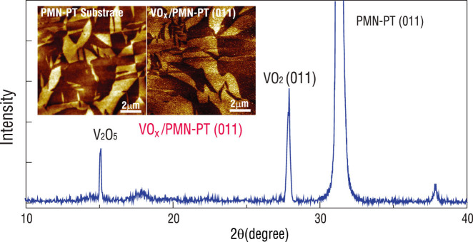
Insets are the out-of-plane PFM phase images of the pristine PMN-PT substrate (left) and the VOx film coated on PMN-PT (right).
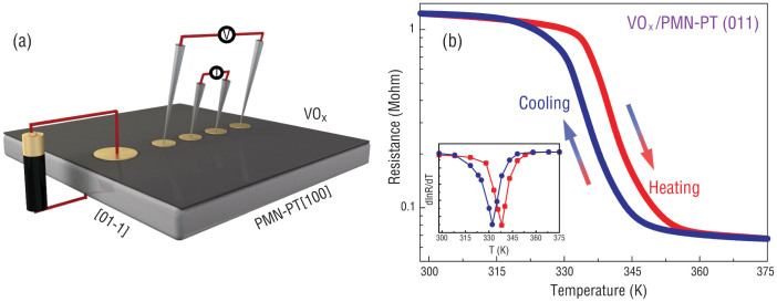
Figure 2 (a) shows the schematics of the experimental setup for the resistivity measurement with a bias electric field applied along the direction perpendicular to the PMN-PT (011) plane. The resistivity of the as-deposited VOx thin film was measured using a four-probe technique in a probe station with a temperature-controlled chuck. The whole piece of the sample was poled by a sufficiently high electric field before carrying out any subsequent electrical measurements. Figure 2 (b) shows the hysteretic temperature dependence of the resistivity measured in the poled VOx/PMN-PT(011) heterostructrues. The resistance of the film changes by as large as one order of magnitude, while the sample undergoes the metal-insulator transition (MIT) within the temperature range of 330 K ~ 350 K. The MIT temperatures for various thermal processes were determined by the first derivative of resistivity versus temperature (the inset in Figure 2b), which are 338 K upon heating and 332 K upon cooling, respectively.
Figure 2.
(a) Schematic of four-point resistance measurement of VOx thin film on a (011)-oriented PMN-PT single crystal substrate. The polling of the PMN-PT was achieved by applying an electric field in the [011] direction. (b) The measured resistance hysteresis loop of the VOx film as a function of temperature. The inset shows the differential curve of the VOx resistance as a function of temperature.
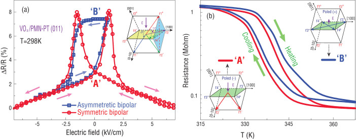
The electric field modulation of the resistivity of VOx with different voltage switching pathways was characterized at room temperature (298 K), as shown in Figure 3 (a). An in-situ voltage was applied on a VOx/PMN-PT sample along the thickness direction, where the VOx film acted as the top electrode and the Au film coated on the backside of the PMN-PT substrate was used as the bottom electrode. Since the resistivity of the VOx thin film is much less than that of the PMN-PT bulk substrate, most of the applied voltage was homogeneously loaded on the PMN-PT substrate and thereby enabled a coherent lattice strain. Upon cycling a triangular electric field with an amplitude of 8 kV/cm, a ‘butterfly' curve (red) of the resistance vs. electric field was displayed (Fig. 3a), showing a relative resistance change of 8% at room temperature, which was defined as  . This result is consistent with the typical ‘butterfly' curve of the strain vs. electric field expected for the PMN-PT substrate, indicating that the resistance change in the VOx films was induced by the lattice strain. In this symmetric bipolar electric field scenario (the strengths of the positive and negative fields are equal), the polarization that undergoes 109° and 180° ferroelectric switching at the coercive fields (inset in Fig. 3a) failed to create the distinct remnant strain states due to the strain equivalence in these domain states. However, upon increasing the strength of the electric field, a strong in-plane anisotropic biaxial strain can be generated, which resulted in the large changes in the resistivity of the VOx films. This strain effects are caused by the linear piezo-effect of the PMN-PT rather than the domain switching.
Figure 3.
(a) The film resistance change induced by symmetric and asymmetric bipolar electric field sweeping at room temperature. The arrows indicate the directions of electric field sweeping. With the application of an asymmetric bipolar electric field, two stable film resistance states ‘A' and ‘B' can be realized. The inset is the schematics of 109°, 71° and 180° polarization switching induced by applying a negative voltage on a positively poled PMN-PT(011) substrate. (b) The film resistance as a function of temperature under two different poled states, where the polarization points to the out-of-plane direction (left inset) and stays in the (011) plane (right inset). These two strain states ‘A' and ‘B' correspond to the two remanant resitivity states.
When an asymmetric bipolar electric field was applied (the negative field is larger and the positive field is smaller), a hysteretic response of the resistance vs. the electric field was observed. In particular, a dramatic enhancement of the resistance of VOx was found once a small positive electric field of 1.5 kV/cm was applied on a negatively poled PMN-PT substrate and then removed. Moreover, the resistance of VOx could be switched back to its initial state by applying another small negative electric field. In this process, we assume that the 71° ferroelectric/ferroelastic domain switching takes place, which enables the polarization to dynamically rotate between the out-of-plane and the in-plane directions, thus resulting in a significant lattice strain in the (011) plane (inset in Fig. 3a). In this case, two distinct remnant resistance states which are noted as ‘A' for the low resistance state and ‘B' for the high resistance state of VOx were established by reversing the electric field at the coercive field of the PMN-PT. Therefore, domain-engineered ferroelectric/ferroealstric switching can be used for the non-volatile tuning of resistivity in the VOx/PMN-PT heterostructures.
Besides the electric field-induced tuning of the resistivity of VOx at room temperature, the metal-insulator transition temperature of the VOx film on PMN-PT also can be modified by changing the ferroelastic strain states through the application of an electric field, as shown in Figure 3 (b). It is well known that in the metal-insulator transition, the structure of VOx changes from monoclinic at low temperature to tetragonal at high temperature. The spontaneous dilatational strain involved in the transformation is about 0.044%, which is much smaller than a typical piezo-strain of 0.2 ~ 0.5%. Once the vanadium cations pair up along the c-axis, the Mott insulator phase appears. Thus, the MIT temperature is closely related to the c-axis length of the lattice in VOx. In our case, the VOx films with the preferred orientation of [001] for VO2 phase are subject to a compressive strain and tensile strain along the in-plane [100] and [0–11] direction of PMN-PT, respectively. These strains may result in an elongation of the lattice along the c-axis, which is expected to be ~0.2%18. By precisely controlling the ferroelectric domain structure and the lattice strain states, the V-V bond length along the c-axis in the VOx films can be in situ modulated which, in turn, results in the changes in the MIT temperature. In our study, electrically tuning of the metal-insulator transition temperature in VOx/PMN-PT was revealed through the observation of the temperature dependent resistance change in the VOx films at two different poling or strain states of PMN-PT. These two strain states ‘A' and ‘B' correspond to the two remnant resistant states in Fig. 3(a). Given the rhombohedral symmetry of the single crystal PMN-PT, the spontaneous polarization shows eight orientation states (r1+, r1−, r2+, r2−, r3+, r3−, r4+, and r4−) which correspond to four ferroelastic domains (r1, r2, r3, r4). The state ‘A' refers to the negatively poled state (r1/r2), in which all the polarizations point to the out-of-plane by vertically applying a large electric field on the sample and then switching it off (left inset in Fig. 3b). The state ‘B' refers to a “depoled” state (r3/r4), in which most of the polarizations lie in the plane, which was produced by applying a small positive electric field on the negatively poled VOx/PMN-PT and then switching it off. The metal-insulator transition temperature is taken as the midpoint of the sharp jump in the resistance curve upon heating. The transition temperature of VOx rises noticeably by 6 K when the PMN-PT strain state is switched from state “A” to “B”. Since the transition temperature of VO2 is highly sensitive to its c-axis length, the strong out-of-plane strain or lattice distortion produced by the ferroelastic switching of PMN-PT shows a great capability to modify the transition temperature of VOx. The stable and reversible in-plane and out-of-plane polarization states enable the control of the transition temperature of the VOx on the PMN-PT substrate by simply switching the electric field, which offers an energy efficient way to control the MIT property of VOx.
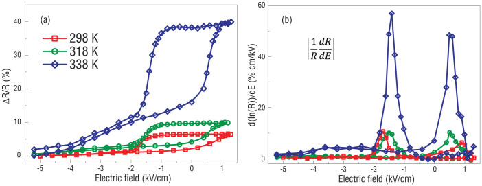
Figure 4(a) shows that the electric fields in-situ manipulate the resistance in VOx/PMN-PT (011) at various temperatures. Hysteretic changes in the resistance were observed upon applying appropriate asymmetric bipolar electric fields, showing a large tunability with an up to 40% change in the resistance at the transition temperature of 338 K (8% at room temperature). This indicates that the resistivity is very sensitive to the external strain induced by the electric field near the MIT. Figure 4(b) shows the first derivatives of ln(R) with respect to the applied electric field (E) across the sample at various temperatures. A giant resistance change coefficient, defined as d(ln(R))/dE, was observed, which is up to 55%. cm/kV at the MIT temperature as the polarization vectors were electrically switched between the in-plane and out-of-plane states at the coercive fields. The sharpness of the peaks in d(ln(R))/dE and the lower coercive fields at room temperature are ideal for device applications. Conversely, at low T the broad peaks and higher coercive fields point to a relatively difficult ferroelectric polarization switching in the PMN-PT.
Figure 4.
(a) The film resistance change induced by asymmetric bipolar electric fields at different temperatures. The largest voltage induced resistance change was observed in 338 K, which corresponds to the phase transition temperature of the VOx thin film. (b) The first derivative of the hysteretic resistance with respect to electric field, as a function of electric field at different temperatures.
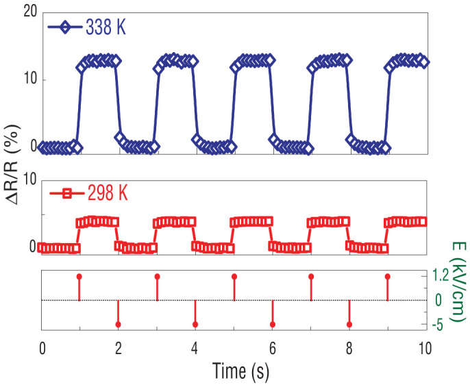
Figure 5 shows the electric field impulse-induced non-volatile switching of the resistance in VOx/PMN-PT at room temperature and at the MIT transition temperature of 338 K. Upon the application of an appropriate electric field impulse, non-volatile switching of the resistance in VOx/PMN-PT heterostructures has been realized, corresponding to the two distinct stable and reversible strain states. The electric field-induced modulations of the resistance reached 13% and 4% at 338 K and at room temperature, respectively. The change of the resistance of VOx did not show any noticeable variation after 2000 cycles.
Figure 5. The voltage impulse induced non-volatile resistance switching at the phase transition temperature and room temperature.
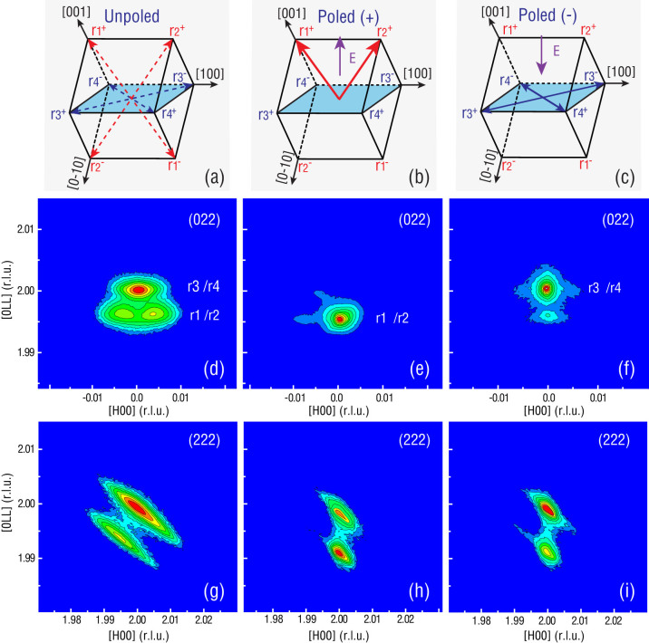
In order to confirm that the non-volatile switching of the conductivity in the VOx films comes from the stable and reversible polarization rotation in the PMN-PT (011) substrates, a high resolution x-ray reciprocal space mapping (RSM) technique was used to quantitatively determine the polarization switching pathway in response to the electric fields. Figure 6 shows the RSMs of the PMN-PT (011) substrate in the vicinity of the (022) and (222) reflections under various poling states. Due to the rhombohedral symmetry in the PMN-PT single crystal, four possible strain states (r1, r2, r3, r4) exist, as shown in Fig. 6(a). According to the lattice parameter and the rhombohedral domain structure, r1/r2 and r3/r4 can be distinguished by the different spot distributions and intensities in the (022) reflection. Meanwhile, r2 and r1/r3/r4 can be distinguished by the different spot distributions in the (222) reflection. Analysis of the RSM patterns in the initial state (Figure 6d and 6g) suggests that all the possible domain states coexist with most of the polarizations lying in the (022) plane. After a positive voltage was applied on the sample, the RSM in Figure 6e shows a single high intensity reflection spot with a lower Q022 value, while the spot with the high Q022 value disappears. This high intensity spot corresponds to the r1/r2 domain states, with all the polarizations pointing to the out-of-plane direction. The domain distribution of r1 and r2 can be quantitatively determined from the (222) reflection shown in Figure 6h. After an appropriate negative electric field is applied and removed, the spot with the lower Q022 value almost vanishes, while the spot with the high Q022 value appears, as shown in Figure 6f, indicating that the polarization undergoes a 71° domain switching and its vectors are rotated from the out-of-plane directions to the in-plane directions. Therefore, the stable and reversible ferroelectric/ferroelastic domain switching pathway is confirmed, which arises from the polarization rotation between the in-plane and the out-of-plane directions. Analysis of the peak intensities revealed that the 71° domain switching takes place in up to 90% of the entire poled area, leading to a large homogeneous in-plane lattice strain. This points out the advantage of poling a (011)-oriented PMN-PT over a (001)-oriented PMN-PT where only the 109° domain switching facilitates the in-plane lattice strain and it merely covers 26% of the poled area.
Figure 6. Schematics of domain structures and reciprocal space maps (RSMs) about the (022) and (222) reflections of PMN-PT(011) under various applied electric fields or poling states.
The first column (a), (d), (g) is for the unpoled state. The second column (b), (e), (h) is for the positive poling state with up to 90% of polarization pointing upward. The third column (c), (f), (i) is after applying an negative electric field of −1.5 kV/cm and then switching it off. Electric-field-induced ferroelastic polarization switching between the in-plane direction and the out-of-plane directions is clearly demonstrated in the RSM patterns of the (022) reflection (e), (f).
Discussion
The electric field modulation of the metal-insulator transition and the non-volatile switching of the resistivity have been demonstrated in the VOx/PMN-PT (011) heterostructures. A variation of the transition temperature up to 6 K is realized via two distinct, stable and reversible strain states generated by using a unique ferroelastric switching pathway. Although the VOx film used in this work shows a poor phase quality, a distinct property tuning of VOx with applying a voltage was observed. It can be expected that if the epitaxial VO2 film with the resistance change more than 4 orders of magnitude are grown on the PMN-PT or other ferroelectric substrate, the electrical tuning of the resistance will be much more distinguished. This voltage impulse tuning of the metal-insulator transition shows a great potential for the application of next generation fast, energy-efficient, reconfigurable electronic devices.
Method
The VOx films were deposited on the (011)-oriented PMN-PT substrates by using the RF-magnetron sputtering. The substrates were kept at 500°C and the deposition process took place in an Ar and O2 mixed atmosphere at a pressure of 3 mTorr. The power of the RF gun was set to be 150 W. The thickness of the VOx film was about 100 nm by controlling the deposition time. Four circular Au top electrodes with a diameter of 200 μm were sputtered on the VOx film using a shadow mask. The structure and surface of the films were characterized with a high-resolution x-ray diffraction (XRD) and piezoresponse force microscopy (PFM). The electric transport properties were measured by the four-point measurement at different temperatures in a probe station with a temperature controlled chuck. The in-situ electric field was applied along the thickness direction of the PMN-PT substrates. The domain structure in the PMN-PT (011) were characterized in reciprocal space mapping (RSM) using a triple axis diffractometer under different switching pathways.
Author Contributions
M.L. and T.N. initiated the original idea and planed the experiments. T.N. and M.L. prepared and performed all the experiments. The paper was written by M.L. and T.N. M.L., T.N., W.R., Z.Y. and N.S. discussed the data and the results, and commented the manuscript.
Supplementary Material
Supplementary Information
Acknowledgments
The work in China was supported by the Natural Science Foundation of China (Grant No. 90923001), the International Science & Technology Cooperation Program of China (Grant Nos. 2010DFB13640 and 2011DFA51880), the National 111 Project of China (B14040), the Fundamental Research Funds for the Central Universities. Ming Liu was supported by the China Young 1000-Talent Program. The work in USA was supported by AFRL through UES Subcontract No. S-875-060-018, Semiconductor Research Corporation, and National Natural Science Foundation of China (NSFC) 51328203. The work at SFU was supported by the U.S. Office of Naval Research (Grant No. N00014-12-1-1045) and the Natural Science and Engineering Research Council of Canada. The authors thank the contribution of Ms. Liangchuan Sun on 3D schematics.
References
- Inoue I. H. & Rozenberg M. J. Taming the Mott transition for a novel Mott transistor. Adv. Funct. Mater. 18, 2289–2292 (2008). [Google Scholar]
- Yang Z., Ko C. Y. & Ramanathan S. Oxide Electronics Utilizing Ultrafast Metal-Insulator Transitions. Annu. Rev. Mater. Res. 41, 337–367 (2011). [Google Scholar]
- Theis T. N. & Solomon P. M. It's Time to Reinvent the Transistor!. Science 327, 1600–1601 (2010). [DOI] [PubMed] [Google Scholar]
- Ahn K. H., Lookman T. & Bishop A. R. Strain-induced metal-insulator phase coexistence in perovskite manganites. Nature 428, 401–404 (2004). [DOI] [PubMed] [Google Scholar]
- Ahn C. H., Triscone J. M. & Mannhart J. Electric field effect in correlated oxide systems. Nature 424, 1015–1018 (2003). [DOI] [PubMed] [Google Scholar]
- Zylbersztejn A. & Mott N. F. Metal-insulator transition in vanadium dioxide. Phys. Rev. B 11, 4383–4395 (1975). [Google Scholar]
- Aetukuri N. B. et al. Control of the metal-insulator transition in vanadium dioxide by modifying orbital occupancy. Nat. Phys. 9, 661–666 (2013). [Google Scholar]
- Park J. H. et al. Measurement of a solid-state triple point at the metal-insulator transition in VO2. Nature 500, 431–434 (2013). [DOI] [PubMed] [Google Scholar]
- Cao J. et al. Strain engineering and one-dimensional organization of metal-insulator domains in single-crystal vanadium dioxide beams. Nat. Nanotechnol. 4, 732–737 (2009). [DOI] [PubMed] [Google Scholar]
- Scherwitzl R. et al. Electric-Field Control of the Metal-Insulator Transition in Ultrathin NdNiO3 Films. Adv. Mater. 22, 5517–5520 (2010). [DOI] [PubMed] [Google Scholar]
- Nan C. W., Bichurin M. I., Dong S. X., Viehland D. & Srinivasan G. Multiferroic magnetoelectric composites: Historical perspective, status, and future directions. J. Appl. Phys. 103, 031101 (2008). [Google Scholar]
- Vaz C. A. F., Hoffman J., Anh C. H. & Ramesh R. Magnetoelectric Coupling Effects in Multiferroic Complex Oxide Composite Structures. Adv. Mater. 22, 2900–2918 (2010). [DOI] [PubMed] [Google Scholar]
- Shi J., Ha S. D., Zhou Y., Schoofs F. & Ramanathan S. A correlated nickelate synaptic transistor. Nat. Commun. 4, 2676 (2013). [DOI] [PubMed] [Google Scholar]
- Nakano M. et al. Collective bulk carrier delocalization driven by electrostatic surface charge accumulation. Nature 487, 459–462 (2012). [DOI] [PubMed] [Google Scholar]
- Wei J., Wang Z., Chen W. & Cobden D. H. New aspects of the metal-insulator transition in single-domain vanadium dioxide nanobeams. Nat. Nanotechnol. 4, 420–424 (2009). [DOI] [PubMed] [Google Scholar]
- Lee J. H. & Rabe K. M. Coupled Magnetic-Ferroelectric Metal-Insulator Transition in Epitaxially Strained SrCoO3 from First Principles. Phys. Rev. Lett. 107, 067601 (2011). [DOI] [PubMed] [Google Scholar]
- Schlom D. G. et al. Strain tuning of ferroelectric thin films. Annu. Rev. Mater. Res. 37, 589–626 (2007). [Google Scholar]
- Liu M. et al. Non-volatile ferroelastic switching of the Verwey transition and resistivity of epitaxial Fe3O4/PMN-PT (011). Sci. Rep. 3, 1867 (2013). [DOI] [PMC free article] [PubMed] [Google Scholar]
- Qazilbash M. M. et al. Mott transition in VO2 revealed by infrared spectroscopy and nano-imaging. Science 318, 1750–1753 (2007). [DOI] [PubMed] [Google Scholar]
- Viswanath B. & Ramanathan S. Direct in situ observation of structural transition driven actuation in VO2 utilizing electron transparent cantilevers. Nanoscale 5, 7484–7492 (2013). [DOI] [PubMed] [Google Scholar]
- Jeong J. et al. Suppression of Metal-Insulator Transition in VO2 by Electric Field–Induced Oxygen Vacancy Formation. Science 339, 1402–1405 (2013). [DOI] [PubMed] [Google Scholar]
- Baek S. H. et al. Ferroelastic switching for nanoscale non-volatile magnetoelectric devices. Nat. Mater. 9, 309–314 (2010). [DOI] [PubMed] [Google Scholar]
- Dale D., Fleet A., Brock J. D. & Suzuki Y. Dynamically tuning properties of epitaxial colossal magnetoresistance thin films. Appl. Phys. Lett. 82, 3725–3727 (2003). [Google Scholar]
- Ma J., Hu J. M., Li Z. & Nan C. W. Recent Progress in Multiferroic Magnetoelectric Composites: from Bulk to Thin Films. Adv. Mater. 23, 1062–1087 (2011). [DOI] [PubMed] [Google Scholar]
- Eerenstein W., Wiora M., Prieto J. L., Scott J. F. & Mathur N. D. Giant sharp and persistent converse magnetoelectric effects in multiferroic epitaxial heterostructures. Nat. Mater. 6, 348–351 (2007). [DOI] [PubMed] [Google Scholar]
- Liu M. et al. Giant Electric Field Tuning of Magnetic Properties in Multiferroic Ferrite/Ferroelectric Heterostructures. Adv. Funct. Mater. 19, 1826–1831 (2009). [Google Scholar]
- Srinivasan G. Magnetoelectric Composites. Annu. Rev. Mater. Res. 40, 153–178 (2010). [Google Scholar]
- Spaldin N. A., Cheong S. W. & Ramesh R. Multiferroics: Past, present, and future. Phys. Today 63, 38–43 (2010). [Google Scholar]
- Hu J. M., Li Z., Chen L. Q. & Nan C. W. Design of a Voltage-Controlled Magnetic Random Access Memory Based on Anisotropic Magnetoresistance in a Single Magnetic Layer. Adv. Mater. 24, 2869–2873 (2012). [DOI] [PubMed] [Google Scholar]
- Wu T. et al. Electric-poling-induced magnetic anisotropy and electric-field-induced magnetization reorientation in magnetoelectric Ni/(011) [Pb(Mg1/3Nb2/3)O3](1-x)-[PbTiO3]x heterostructure. J. Appl. Phys. 109, 07D732 (2011). [Google Scholar]
- Nan T. X., Hui Y., Rinaldi M. & Sun N. X. Self-Biased 215 MHz Magnetoelectric NEMS Resonator for Ultra-Sensitive DC Magnetic Field Detection. Sci. Rep. 3, 1985 (2013). [DOI] [PMC free article] [PubMed] [Google Scholar]
- Liu M. et al. Electric field modulation of magnetoresistance in multiferroic heterostructures for ultralow power electronics. Appl. Phys. Lett. 98, 222509 (2011). [Google Scholar]
- Nan T. X. et al. Voltage impulse induced bistable magnetization switching in multiferroic heterostructures. Appl. Phys. Lett. 100, 132409–132403 (2012). [Google Scholar]
- Liu J. M. & Nan C. W. Ferroelectricity and multiferroicity: Broader way to go beyond. Front. Phys. 7, 373–374 (2012). [Google Scholar]
- Ohno H. A window on the future of spintronics. Nat. Mat. 9, 952–954 (2010). [DOI] [PubMed] [Google Scholar]
- Bozovic I., Logvenov G., Belca I., Narimbetov B. & Sveklo I. Epitaxial Strain and Superconductivity in La2-xSrxCuO4 Thin Films. Phys. Rev. Lett. 89, 107001 (2002). [DOI] [PubMed] [Google Scholar]
- Zhao P. et al. Fabrication and characterization of all-thin-film magnetoelectric sensors. Appl. Phys. Lett. 94, 243507 (2009). [Google Scholar]
- Zhang S. et al. Electric-Field Control of Nonvolatile Magnetization in Structure at Room Temperature. Phys. Rev. Lett. 108, 137203 (2012). [DOI] [PubMed] [Google Scholar]
- Bilani-Zeneli O. et al. SrTiO3 on piezoelectric PMN-PT(001) for application of variable strain. J. Appl. Phys. 104, 054108–054105 (2008). [Google Scholar]
- Zheng R. K., Habermeier H.-U., Chan H. L. W., Choy C. L. & Luo H. S. Effects of substrate-induced strain on transport properties of LaMnO3 and CaMnO3 thin films using ferroelectric poling and converse piezoelectric effect. Phys. Rev. B 81, 1–9 (2010). [Google Scholar]
- Zheng R. K., Wang Y., Chan H. L. W., Choy C. L. & Luo H. S. Substrate-induced strain effect in La0.875Ba0.125MnO3 thin films grown on ferroelectric single-crystal substrates. Appl. Phys. Lett. 92, 082908 (2008). [Google Scholar]
- Thiele C., Dörr K., Bilani O., Rödel J. & Schultz L. Influence of strain on the magnetization and magnetoelectric effect in La0.7A0.3MnO3/PMN-PT(001) (A = Sr,Ca). Phys. Rev. B 75, 054408 (2007). [Google Scholar]
- Liu M. et al. Voltage-Impulse-Induced Non-Volatile Ferroelastic Switching of Ferromagnetic Resonance for Reconfigurable Magnetoelectric Microwave Devices. Adv. Mater. 25, 4886–4892 (2013). [DOI] [PubMed] [Google Scholar]
- Nan T. X. et al. Quantification of Strain and Charge Co-mediated Magnetoelectric Coupling on Ultra-thin Permalloy/PMN-PT Interface. Sci. Rep. 4, 3688 (2014). [DOI] [PMC free article] [PubMed] [Google Scholar]
Associated Data
This section collects any data citations, data availability statements, or supplementary materials included in this article.
Supplementary Materials
Supplementary Information


