Abstract
Resistive switching memories (RRAMs) are attractive for replacement of conventional flash in the future. Although different switching materials have been reported; however, low-current operated devices (<100 μA) are necessary for productive RRAM applications. Therefore, TaOx is one of the prospective switching materials because of two stable phases of TaO2 and Ta2O5, which can also control the stable low- and high-resistance states. Long program/erase endurance and data retention at high temperature under low-current operation are also reported in published literature. So far, bilayered TaOx with inert electrodes (Pt and/or Ir) or single layer TaOx with semi-reactive electrodes (W and Ti/W or Ta/Pt) is proposed for real RRAM applications. It is found that the memory characteristics at current compliance (CC) of 80 μA is acceptable for real application; however, data are becoming worst at CC of 10 μA. Therefore, it is very challenging to reduce the operation current (few microampere) of the RRAM devices. This study investigates the switching mode, mechanism, and performance of low-current operated TaOx-based devices as compared to other RRAM devices. This topical review will not only help for application of TaOx-based nanoscale RRAM devices but also encourage researcher to overcome the challenges in the future production.
Keywords: Resistive switching, Memory, TaOx, RRAM
Review
Background
Semiconductor memory is an essential component of today’s electronic systems. It is used in any equipment that uses a processor such as computers, smart phones, tablets, digital cameras, entertainment devices, global positioning systems, automotive systems, etc. Memories constituted 20% of the semiconductor market for the last 30 years and are expected to increase in the coming years [1]. Generally, memory devices can be categorized as 'volatile’ and 'non-volatile’ based on their operational principles. A volatile memory cannot retain stored data without the external power whereas a non-volatile memory (NVM) is the one which can retain the stored information irrespective of the external power. Static random access memory and dynamic random access memory (DRAM) fall into the volatile category, while 'Flash’ which is the short form of 'flash electrically erasable programmable read-only memory’ is the dominant commercial NVM technology. The requirements of an ideal NVM are high density, scalability, low cost, low-energy operation, and high performance for potential applications. Today’s dominant memory technologies are DRAM and Flash, both have scaling issues. The DRAM offers very high endurance (approximately 1014 cycles); however, the endurance of Flash is limited (approximately 106 cycles), and the operation is slow as the program/erase time is relatively high (microseconds up to milliseconds). Generally, it needs high voltage for program and erase operations (>׀10 ׀V) [2,3]. In order to overcome these problems, other non-volatile memories such as ferroelectric RAM (FeRAM) [4,5], magnetic RAM (MRAM) [6,7], phase-change-memory (PCM) [8], and resistive RAM (RRAM) are being investigated [9-25]. The basic memories, prototypical, and emerging memories with respect to various performance parameters from International Technology Roadmap for Semiconductors (ITRS) in 2012 have been compared [26]. All these memories store data by resistance change in contrast to charge as in basic memories. In FeRAM, the polarization direction of the dipoles in the ferroelectric layer can be switched by applying the electric field which, in turn, leads the different memory states. MRAM utilizes the orientation of magnetization of a small magnetic element by the application of magnetic field which gives rise to the change in the electric resistance and enable data bits to be stored. Although, FeRAM and MRAM both have fast switching (<20 ns) and long endurance (>1015 cycles), these memories show insufficient scalability [27]. Moreover, MRAM needs high programming current (in the range of milliampere) [6]. Compared to FeRAM and MRAM, PCM offers greater potential for future application because of its better scalability [27]. In principle, PCM heats up a material changing it from low-resistance polycrystalline phase to a high-resistance amorphous phase reversibly. So in PCM, the generated heat, i.e., thermal effect, controls the switching. Due to this, the PCM cell needs more power for switching which limits its application in low-power devices. All memories discussed above are in production, though RRAM is at its early maturity level and it shows excellent potential to meet ITRS requirements for next-generation memory technology. Apart from its non-volatility, it shows good scalability potential below 10 nm. Some of the RRAM advantages are summarized in schematic diagram (Figure 1). Ho et al. [28] has demonstrated a 9-nm half-pitch RRAM device. They showed that if high-density vertical bipolar junction transistor will be used as a select transistor, it cannot provide the programming current required for PCRAM below 40 nm while for RRAM, it can be used even below 10 nm. Park et al. [20] reported sub-5-nm device in a Pt/TiO2/Cu structure. Ultra-high-speed operation of RRAM using atomic layer deposited HfO2 switching material is reported by Lee et al. [29], where a 300-ps pulse of only 1.4 V, successfully switches the device without any change in memory window. Torrezan et al. [21] also demonstrated the fast switching speed of 105 ps. Low energy consumption of only 0.1 pJ per operation [25] and multi-level data storage [16] required for high-density integration were reported. The energy consumption can be further reduced with increased reliability by scaling it to smaller dimensions [30]. Long pulse endurance of >1012 cycles is also demonstrated in TaOx-based crossbar device [31]. Other incentives of RRAM include its simple metal-insulator-metal (MIM) structure and good complementary metal-oxide-semiconductor (CMOS) compatibility. However, the poor understanding of the switching reliability, mechanism, low-current operation (<100 μA) are the bottlenecks in its further development and optimization. Overall, on the light of above discussion, RRAM is one of the most promising candidates for the replacement of flash in future. On the other hand, RRAM can also find its own application area, which will be more challenging and useful in the near future. Furthermore, the TaOx-based RRAM devices have been also reported extensively in the literature and shown good resistive switching performance. It is expected that this TaOx-based RRAM device has strong potential for production in near future. However, the TaOx-based RRAM devices with prospective and challenges have not been reviewed in literature yet.
Figure 1.
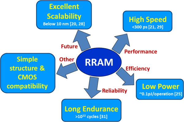
Prospective of RRAM devices. Endurance, speed, scalability, and requirements of RRAM devices.
This topical review investigates the switching mode, mechanism, and performances of the TaOx-based devices as compared to other RRAMs in literature. Long program/erase endurance and data retention of >85°C with high yield have a greater prospective of TaOx-based nanoscale RRAM devices; however, lower current (few microampere) operation is very challenging for practical application, which is reviewed in detail here.
Resistive RAM overview
Resistance switching effect was first reported by Hickmott in 1962 [32] and had subsequently been observed by many researchers over the years [9-36]. RRAM is a two-terminal passive device in which a comparatively insulating switching layer is sandwiched between two electrically conducting electrodes, as shown in Figure 2. However, a working RRAM device generally consists of one transistor (1T) or one diode (1D) and one resistor (1R), i.e., 1T1R or 1D1R configurations. The resistance of the RRAM device can be altered by simply applying external bias across the MIM stack. The electrode on which a voltage or current is applied can be referred to as the top electrode (TE), and the other electrically grounded electrode can be called as the bottom electrode (BE).
Figure 2.
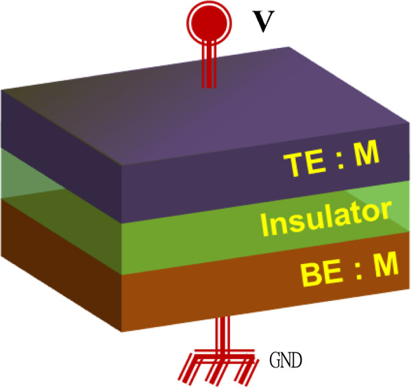
Structure of RRAM device. Schematic diagram of RRAM in metal-insulator-metal structure and its biasing.
Switching modes: unipolar/bipolar
The resistance of a RRAM device can be modulated in two ways as shown by the current/voltage (I-V) curves in Figure 3. On the basis of I-V curves, the switching modes can be classified as unipolar (nonpolar) and bipolar. In unipolar resistive switching mode (Figure 3a), the switching direction does not depend on the polarity of the applied voltage and generally occurs at higher voltage amplitude that of bipolar switching. A pristine memory device with high initial resistance state (IRS) can be switched in to a low-resistance state (LRS) by applying a high voltage stress. This process is called the 'electroforming process’ or simply 'forming process’ and alters the resistance of the pristine device irreversibly [15,37]. Some RRAM devices do not need the forming process and are called forming-free devices. Forming-free devices are highly required for RRAM practical application and are reported infrequently [38-41]. After the forming process, the RRAM device can be switched to a high-resistance state (HRS), generally lower than that of the IRS by the application of a particular voltage called reset voltage. This process is called 'RESET process.’ Switching from a HRS to a LRS called 'SET.’ In the SET process, generally, the current is limited by the current compliance (CC) in order to avoid device damage. The resistive switching in unipolar mode has been observed in many highly insulating oxides, such as binary metal oxides [10]. The unipolar devices suffer from high non-uniformity and poor endurance. In bipolar resistive switching mode, the SET and RESET occur in the opposite polarity, i.e., if memory device can be set by applying positive voltage on TE, then only negative voltage can reset the device (Figure 3b). So, this type of resistive switching is sensitive to the polarity of the applied voltage. For bipolar switching to occur, the MIM stack should be asymmetric generally, such as different electrodes or a dedicated voltage polarity for the forming process. Many oxides show bipolar resistive switching and will be also discussed later. The devices in which unipolar and bipolar modes can be changed by changing the operation conditions are called 'nonpolar’ devices [42], and the resistive switching mechanism is explained below.
Figure 3.
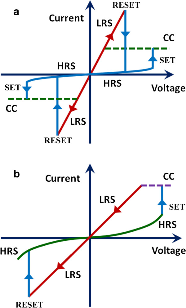
Switching mode of the RRAM devices. (a) I-V curves for unipolar (nonpolar) switching where the switching direction is independent on the polarity of the applied voltage and (b) bipolar switching. In bipolar switching, SET and RESET occur at opposite polarity bias.
Resistive switching mechanism
Generally, depending on the conduction path, the switching mechanism can be classified as (1) filamentary-type and (2) interface-type, as shown in Figure 4. In the filamentary model, the switching originates from the formation/rupture of conducting filament in the switching material by the application of suitable external bias shown in Figure 4a [15,17]. The filamentary paths are formed under SET and ruptured under RESET. Electrochemical migration of oxygen ions and redox reaction near the metal/oxide interface is widely considered as the possible mechanism behind the formation and rupture of the filaments [43]. However, clear visualization of the conducting filaments in switching material has yet to be achieved. Studies involving high-resolution transmission electron microscopy showed the conducting filaments in different systems [24,44-48]; however, the switching mechanism is still clearly not understood. On the other hand, in the interface-type mechanism, the switching occurs at the interface of the metal and switching material, as shown in Figure 4b [49]. Several models have been reported for the driving mechanism involved in an interface-type conducting path, such as electrochemical migration of oxygen vacancies [50-53], trapping of charge carriers (hole or electron) [54,55], and a Mott transition induced by carriers doped at the interface [56-58]. To understand the difference between the filament and interface types of resistive switching, the area dependence of the RRAM device resistance could be examined. In general, if the resistance of the LRS is independent of the device area and HRS varies inversely, the switching is filamentary. When both LRS and HRS increase with decreasing device area, the switching is related to interface-type.
Figure 4.
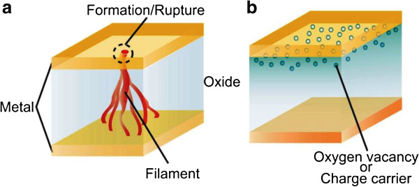
Switching mechanism. (a) Filamentary conducting path model and (b) an interface-type conducting path model [15,17].
Further, depending on the switching material and electrodes, the resistive switching memory can be divided into two types: cation-based switching called electrochemical metallization (ECM) memory and anion-based switching called valance change memory (VCM) [17]. In cation-based memory, a solid-electrolyte was used as a switching material and an electrochemically active metal such as copper (Cu), silver (Ag), and Nickel (Ni) as TE and an inert metal as BE [17]. Generally, the ions of Cu and Ag were known as mobile ions. When positive voltage was applied on the Cu TE, for example, metallic Cu was reduced electrochemically to give Cu+ ions generated from metallic Cu due to anodic dissolution. These ions then diffused through the solid electrolyte due to electric field and reached to the BE where these ions reduced to become metallic Cu and electro-crystallize on the BE. As a result, a conducting filament grew preferentially from the BE and finally bridge the BE and TE. Consequently, the device switched to the LRS. That is the reason that ECM devices were also called conducting bridge RAM. When negative voltage was applied on the TE electrode, the Cu filament broken due to electrochemical dissolution reaction initiated by an electronic current through the metallic bridge, and, in parallel, an electrochemical current and the device came into HRS. In recent years, many solid electrolyte materials such as GeSex[11,59,60], GeS [61,62], Cu2S [63], Ag2S [64], Ta2O5[65,66], SiO2[67], TiO2[68], ZrO2[69], HfO2[70], GeOx[48], MoOx/GdOx[71], TiOx/TaSiOy[72], GeSex/TaOx[46], CuTe/Al2O3[73], and Ti/TaOx[22] were reported. The VCM devices consist of a sub-stoichiometric switching material and an inert electrode such as Pt, Ir, Au, etc., or reactive electrode such as W, Al, Ti, Ni, etc. In VCM devices, switching occurs due to the redox reaction induced by anion (O2-) migration to form conducting filament, as shown in Figure 4a. These devices usually need a forming step in order to switch between LRS and HRS reversibly [17,21]. During electroforming process, the generation of oxygen O2- ions occurs in the switching material due to chemical bond breaking. The generated O2- ions migrate toward the TE under the external bias, and oxygen gas evolution at the anode due to anodic reaction are also reported in literature. To maintain the charge neutrality, the valance state of the cations changes. Therefore, it is called VCM memory. Due to O2- ion generation and anodic reaction, oxygen vacancy conducting path generates in the switching material between TE and BE, and device switches to LRS. The electroforming conditions strongly depend on the dimension of the sample, in particular, the switching material thickness. In addition, thermal effects play an essential role in the electroforming, and it sometimes damage the devices by introducing morphological changes [17,21]. Partially blown electrodes during forming have been observed [17]. Thus, the high-voltage forming step needs to be eliminated in order to product the RRAM devices in future. However, anion-based switching material with combination of different electrode materials and interface engineering will have good flexibility to obtain proper RRAM device.
RRAM materials
Resistance switching can originate from a variety of defects that alter electronic transport rather than a specific electronic structure of insulating materials, and consequently, almost all insulating oxides exhibit resistance switching behavior. Over the years, several materials in different structures have been reported for RRAM application to have better performance. The switching materials of anion-based devices include transition metal oxides, complex oxides, large bandgap dielectrics, nitrides, and chalcogenides. Table 1 lists some of the important materials known to exhibit resistance switching for prospective applications. Few of them reported low-current operation <100 μA only, which is very challenging for real applications in future. Among other various metal oxides such as NiOx[74-76], TiOx[77-81], HfOx[29,38,82-86], Cu2O [87], SrTiO3[43,88], ZrO2[89-92], WOx[28,30,93], AlOx[94-97], ZnOx[39,98-101], SiOx[102,103], GdOx[104,105], Pr0.7Ca0.3MnO3[15,106], GeOx[107,108], and tantalum oxide (TaOx)-based devices [31,109-128] are becoming attractive owing to their ease of deposition using existing conventional systems, high thermal stability up to 1,000°C [115], chemical inertness, compatibility with CMOS processes, and high dielectric constant (ϵ = 25). Moreover, Ta-O system has only two stable phases of Ta2O5 and TaO2 with large solubility of O (71.43 to 66.67 at.%) above 1,000°C in its phase diagram [129]. This property of TaOx is important in order to achieve long switching endurance (the longest reported endurance of >1012 cycles is from TaOx-based device [31]). It has a metastable and comparatively conducting TaO2 phase. Further, the absolute value of Gibbs free energy for redox (reduction-oxidation) reaction of TaOx is low which shows its better stability [109]. The redox reaction is written in Equation 1 below.
Table 1.
Switching materials and SET/RESET current in published literature
| RRAM materials with structure | Switching mode |
Current |
References | |
|---|---|---|---|---|
| SET | RESET | |||
| Pt/NiO/Pt |
Unipolar |
1 mA |
>1 mA |
Kim et al. [74] |
| Pt/NiO/W |
Unipolar |
~20 μA |
~500 μA |
Ielmini et al. [75] |
| Pt/NiO/Pt |
Bipolar |
3 mA |
~3 mA |
Jousseaume et al. [76] |
| Pt/TiO2/TiO2-x/Pt |
Bipolar |
<200 μA |
<200 μA |
Yang et al. [77] |
| Pt/Ti/TiO2/W and Pt/W/TiO2/W |
Bipolar |
500 μA |
0.5 and 3 mA |
Harmes et al. [78] |
| Ir/TiOx/TiN |
Bipolar |
1 mA |
~2 mA |
Park et al. [79] |
| TiN/TiOx/HfOx/TiN |
Bipolar |
40-200 μA |
40-200 μA |
Lee & Chen et al. [29,38] |
| Pt/ZrOx/HfOx/TiN |
Bipolar |
<200 μA |
~200 μA |
Lee et al. [83] |
| TiN/Ti/HfO2/TiN |
Bipolar |
150 μA |
~100 μA |
Walczyk et al. [84] |
| Ta/HfO2/TiN |
Bipolar |
100 μA |
-- |
Chen et al. [85] |
| TiN/TiON/HfOx/Pt |
Bipolar |
50 μA |
3050 μA |
Yu et al. [86] |
| Ni or Co/Cu2O/Cu |
Unipolar |
~80 μA |
~100 μA |
Chen et al. [87] |
| Au or Pt/SrTiO3/Au or Pt |
Bipolar |
2.8 ± 0.8 mA |
2.5 ± 0.5 mA |
Szot et al. [43] |
| Au/SrTiO3/Ti |
Bipolar |
10 mA |
~2 mA |
Sun et al. [88] |
| Ti/ZrO2/Pt |
Bipolar |
30 mA (self) |
~30 mA |
Lin et al. [89] |
| Cu/ZrO2:Ti/Pt |
Bipolar |
1 mA |
~10 mA |
Liu et al. [90] |
| Ti/ZrO2/Pt |
Bipolar |
5 mA |
~4 mA |
Wang et al. [91] |
| Ti/Mo:ZrO2/Pt |
Bipolar |
<20 mA |
<30 mA |
Wang et al. [92] |
| TiON/WOx/W/TiN |
Bipolar |
100 nA |
1 μA |
Ho et al. [28] |
| TiN/WOx/W |
Unipolar |
-- |
-- |
Chien et al. [93] |
| Pt/WOx/W |
Bipolar |
10 mA |
~10 mA |
Kim et al. [30] |
| Ti/Al2O3/Pt |
Bipolar |
>1 mA |
~7 mA |
Lin et al. [94] |
| Pt/Al2O3/TiN |
Bipolar |
20 μA |
~20 μA |
Wu et al. [96] |
| IrOx/Al2O3/IrOxND/Al2O3/IrOx |
Bipolar |
500 μA |
>1 mA |
Banerjee et al. [97] |
| Cu/ZnO/n+ |
Unipolar |
~500 μA |
~3 mA |
Qinan et al. [39] |
| Pt/Mn:ZnO/Pt |
Unipolar |
5 mA |
~17 mA |
Peng et al. [98] |
| Ti/ZnO/Ti |
Nonpolar |
20 mA |
-- |
Andy et al. [99] |
| Pt/ZnO/Pt |
Bipolar |
3 mA |
~3 mA |
Chiu et al. [100] |
| Au/ZnO/Au |
Bipolar |
10 mA |
~10 mA |
Peng et al. [101] |
| TiW/SiOx/TiW |
Unipolar |
~100 μA |
~200 μA |
Yao et al. [102] |
| n-Si/SiOx/p-Si |
Bipolar |
2 μA |
~100 μA |
Mehonic et al. [103] |
| Pt/Gd2O3/Pt |
Unipolar |
10 mA |
~30 mA |
Cao et al. [104] |
| IrOx/GdOx/WOx/W |
Bipolar |
1 mA |
~1 mA |
Jana et al. [105] |
| Pt/Al/Pr0.7Ca0.3MnO3/Pt |
Bipolar |
1 mA |
~10 μA |
Seong et al. [106] |
| Ni/GeOx/HfON/TaN |
Bipolar |
0.1 μA (self) |
0.3 nA |
Cheng et al. [107] |
| IrOx/Al2O3/GeNWs/SiO2/p-Si |
Bipolar |
20 μA |
22 μA |
Prakash et al. [108] |
| Pt/TaOx/Pt |
Bipolar |
<170 μA |
<170 μA |
Wei et al. [109] |
| IrOx/TaOx/WOx/W |
Bipolar |
1 mA |
627 μA |
Prakash et al. [116] |
| Ta/TaOx/Pt |
Bipolar |
100 μA |
~100 μA |
Yang et al. [110] |
| Pt/Ta2O5-x/TaO2-x/Pt | Bipolar | 200 μA | ~200 μA | Lee et al. [31] |
| (1) |
A schematic potential energy curve for TaOx is reported by Wei et al. [109]. This implies that both the HRS and the LRS of TaOx are stable owing to small difference of Gibbs free energy in between LRS and HRS, and the barrier height between these states is quite high. Due to these benefits of TaOx switching material, it is important to design RRAM for real application. That is why this material has been studied in this review below.
Resistive RAM using TaOx material
A small via size of 150 × 150 nm2 of the W/Ti/TaOx/W and W/TaOx/W structures was fabricated [41]. A high-κ Ta2O5 film with a thickness of ≈7 nm was then deposited by an e-beam evaporator. Then, a thin Ti (≈3 nm) interfacial layer by rf sputtering was deposited. The final devices were obtained after a lift-off process. Memory device structure and thicknesses of all layers were observed by transmission electron microscopy (TEM) with an energy of 200 keV. Figure 5a shows a typical cross-sectional TEM image of the W/TaOx/W structure. The device size is 150 × 150 nm2. The thickness of TaOx layer is 6.8 nm (Figure 5b). Figure 6a shows TEM image of the W/TiOx/TaOx/W structures. The thicknesses of the TiOx and TaOx layers are approximately 3 and 7 nm, respectively. Both films show an amorphous characteristics outside (Figure 6b) and inside (Figure 6c) regions of the via-hole. The device size is approximately 0.6× 0.6 μm2. As Ti removes oxygen from the Ta2O5 film in the W/TiOx/TaOx/W structure, the film becomes more oxygen-deficient TaOx, which is very important to achieve an improved resistive switching. XPS analyses were carried out to determine the oxidation states of all layers after the fabrication process, and the resulting spectra are presented in Figure 7[22,114]. The spectra were simulated using Gaussian-Lorentzian functions. The peak binding energies of Ta2O5 4f7/2 and Ta2O5 4f5/2 electrons for the Ta2O5/W structure were centered at 26.7 and 28.6 eV, respectively (Figure 7a), and the binding energies of Ta 4f7/2 and Ta 4f5/2 electrons were centered at 21.77 and 23.74 eV, respectively. This suggests that the high-κ Ta2O5 film mixed with Ta metal, resulting in a TaOx layer where x< 2.5. This may be due to the reaction of oxygen with the bottom W layer during deposition of the Ta2O5 film. It is very interesting to note that the area ratios of the Ta 4f7/2 and Ta 4f5/2 peaks with respect to the area of the Ta2O5 4f7/2 peak are both 0.03 for the TaOx/W structure, while those of the TiOx/TaOx/W structure are 0.27 and 0.16, respectively (Figure 7b). This means that the Ta content of the TiOx/TaOx/W structure was higher than that of the TaOx/W structure. Furthermore, the binding energy of TiO2 2p3/2 in Ti/TaOx/W structure is 459.57 eV (Figure 7c). As Ti removes oxygen from the Ta2O5 film, the film becomes the more oxygen-deficient TaOx, which is vital to achieve improved resistive switching. The peak binding energies of the W 4f7/2, WO3 4f7/2, W 4f5/2, and WO3 4f5/2 electrons of the TaOx/W structure are centered at 31.6, 36.2, 33.9, and 38.3 eV, respectively (Figure 7d). The area ratios of the WO3 4f7/2 and WO34f5/2 spectra with respect to the area of W 4f7/2 are both 0.03 for the TaOx/W structure, while those for the TiOx/TaOx/W structure are 0.27 and 0.16, respectively (Figure 7e). This suggests that W can be oxidized at the TaOx/W interface when a Ti layer is not present, resulting in a TaOx/WOx/W structure which may have inferior resistive switching properties. When a Ti layer is deposited on the TaOx film, the W layer is prevented from oxidizing at the TaOx/W interface, leading to the formation of a TiOx/TaOx/W structure. Considering the Gibbs free energies of TiO2, Ta2O5, and WO3 films, which are -887.6, –760.5, and -506.5 kJ/mol, respectively, at 300 K [130], the Ti will consume the highest oxygen content owing to its stronger reactivity than those of the other materials, thereby forming Ta-rich (or defective TaOx) film. This also prevents oxidation of the W TE at the TaOx/W interface owing to the migration of oxygen from the underlying films toward the Ti film, which contributes to the improved resistive switching memory performance as described below.
Figure 5.
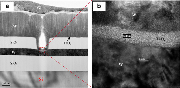
TEM image of W/TaOx/W structure. (a) Cross-sectional TEM image with a device size of 0.15 × 0.15 μm2. (b) HRTEM image inside the via-hole region. The thickness of TaOx film is approximately 6.8 nm.
Figure 6.
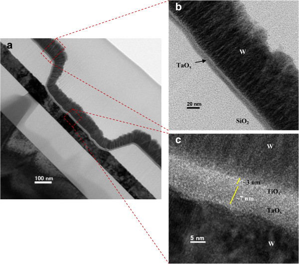
TEM image of W/TiOx/TaOx/W structure. (a) Cross-sectional TEM image with a typical device size of 0.6 × 0.6 μm2. HRTEM images of (b) outside and (c) inside via-hole regions.
Figure 7.
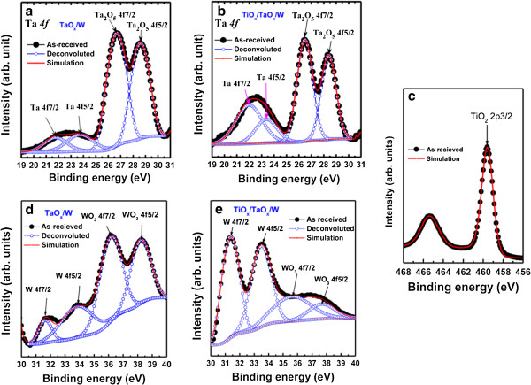
XPS characteristics. Ta 4f spectra for (a) TaOx/W and (b) TiOx/TaOx/W structures. (c) Ti 2p spectrum. W 4f and WO34f spectra for the (d) TaOx/W and (e) TiOx/TaOx/W structures [22,114].
Resistive switching memory characteristics are explained here. Figure 8 shows current/voltage and resistance-voltage characteristics. The W/TiOx/TaOx/W device exhibits >1,000 consecutive repeatable dc switching cycles with a better resistance ratio of 102 under a low CC of 80 μA, the W/TaOx/W device shows few switching cycles with a higher CC of 300 μA [41]. In this case, negatively charged oxygen ions (O2-) migrate from the switching material toward W TE, and this has a lesser possibility to form an oxygen-rich layer at the W TE/TaOx interface, leading to the formation of multi-conduction filaments. However, the insertion of a thin (≈3 nm) Ti layer in between the W and TaOx layers in the W/TiOx/TaOx/W device makes a vast difference because Ti can be used as an oxygen reservoir. A repeatable switching of >10,000 cycles is also observed [41]. Under 'SET,’ O2- rather than oxygen vacancies will migrate from TaOx toward the TE, resulting in a TiO2 layer which controls the conducting vacancy filament diameter in the TaOx layer by controlling current overflow and producing a tighter distribution of the LRS. Owing to this series resistance, the devices exhibit non-ohmic current. It is true that the conducting filament is formed through the TaOx film. When negative voltage is applied to the TE, oxygen ions are pushed from the TiO2 layer toward the conducting filament where they recombine with oxygen vacancies or oxidize the conducting filament. The device will be in HRS. Control of oxygen-deficient filament formation and rupture is facilitated by insertion of the thin Ti layer at the TE/TaOx interface, which results in repeatable and reproducible resistive switching characteristics, which has very good prospective of TaOx-based resistive switching memory in a W/TiOx/TaOx/W structure for real application. Some other reported results have been explained below.
Figure 8.
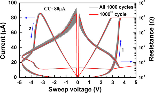
Switching characteristics. Consecutive 1,000 current/voltage and resistance-voltage characteristics of Ti interfacial layer in the W/TiOx/TaOx/W devices [41].
Yang et al. [110] has reported the Pt/TaOx/Ta device with a diameter of 100 μm, where Pt was grounded and external bias was on the Ta electrode. Long program/erase (P/E) endurance of 1.5 × 10¹⁰ cycles with a pulse width of 1 μs is reported. Further, a comparison of endurance characteristics made between TiOx and TaOx-based devices (Figure 9) shows far better performance by TaOx-based devices stretching the P/E cycles to >109 cycles (Figure 9b) as compared to only 104 cycles for TiOx-based devices and it is collapsed finally (Figure 9a). The reason having longer endurance in TaOx devices is the presence of only two solid stable phases in bulk equilibrium with each other and large oxygen solubility in Ta-O system which can act as the source/sink of mobile ions for switching in the insulating phase as compared to many Magneli phases in Ti-O system [110]. The operation current could be reduced to 100 μA. The underlying switching mechanism is attributed to the redox reaction resulting insulating Ta2O5 and conducting Ta(O) solid solution. The energy-filtered TEM (EFTEM) zero-loss images and oxygen map of the switching region confirm also the reduction of TaOx thickness by half in the active region, and the oxygen content in the reduced region is found as low as that in the Ta electrode. The switching phenomenon is believed to be due to oxygen vacancies and ions through nano-ionic transport and a redox process, and this can be called VCM [17]. A schematic diagram was shown in Figure 10a [31,41,43,131-133]. As suggested previously, an intrinsic Schottky barrier exists between the Pt TE and the Ta2O5-x layer contact while in the insulating state, and an ohmic contact is formed in the LRS. This suggests that oxygen ion movement under external bias leads to the LRS to HRS or HRS to LRS. Lee et al. [31] reported TaOx-based crossbar resistive switching memory device. Figure 10b shows the scanning electron microscopy (SEM) image. The device stack consists of Pt top and bottom electrode and bilayer TaOx switching layer with insulating Ta2O5-x layer near TE and TaO2-x near BE as can be seen in the cross-section TEM image presented in Figure 10c. They fabricated the devices with different sizes from 50 × 50 μm2 to 30 × 30 nm2. All size devices have shown self-compliance bipolar switching with small set/rest voltage of -1.0/2.0 V. The switching current of 50 × 50 μm2 device was >200 μA and for 30 × 30 nm2 device was approximately 40 μA, respectively (Figure 10d). From the I-V switching curves, this is a symmetric current profile when the device is in the LRS, but it is an asymmetric current profile for the HRS. This property was exploited to realize RRAM devices in crossbar architecture without any selection device with anti-serial connection. They were also able to achieve the highest ever reported endurance value of 1012 for this system at 30 × 30 μm2 cell size for base layer oxidation of 3%. Data retention of >10 years at 85°C was also reported. To eliminate the need for a discrete switch element such as a diode or transistor, they connected two Pt/Ta2O5-x/TaO2-x/Pt cells antiserially by external contacts and this concept was also reported by Linn et al. [134].
Figure 9.
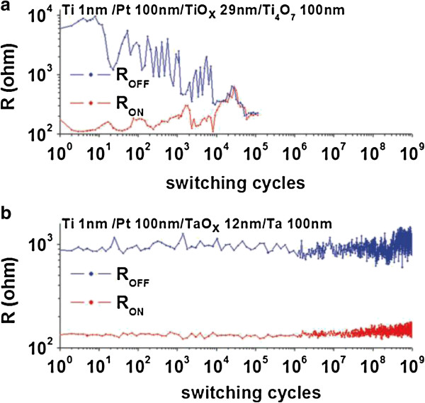
Program/erase endurance. Endurance comparison of (a) TiOx and (b) TaOx devices [110].
Figure 10.
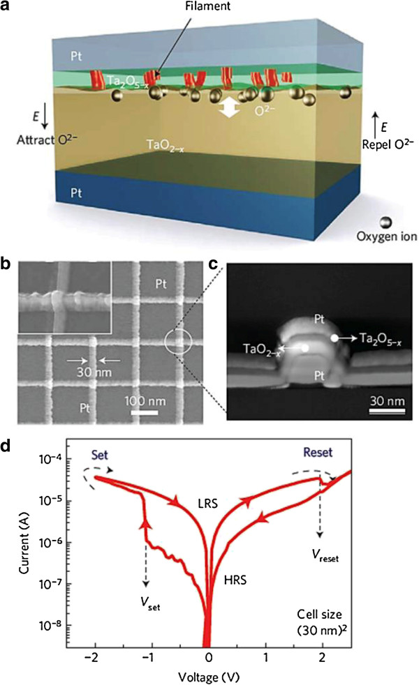
Schematic of switching mechanism and I-V characteristics of cross-point memory devices. (a) Schematic representation of the TaOx device consisting of a thin Ta2O5-x insulating layer and a TaO2-x base layer. The movement of internal oxygen ions or vacancies is used to model the switching. (b) SEM image of a 30-nm crossbar array of devices with the inset showing a single device. (c) TEM cross-section of a 30-nm crossbar cell. The total thickness of TaOx layer is 30 nm. (d) I-V hysteresis characteristics [31].
Wei et al. [109] explored first the prospective application of TaOx-based RRAM devices. The memory stack consisted of Pt top and bottom electrodes and a non-stoichiometric switching layer of TaOx. The first layer near the TE is close to insulating Ta2O5-x phase, while the other layer is close to TaO2-x phase which is conducting. The memory device with a size of 0.5 × 0.5 μm2 in 1T1R configuration showed bipolar switching characteristics under an operation current of approximately 170 μA. The device shows excellent P/E endurance of >109 cycles. The data retention property could be improved under low-current operation by controlling the size of the conductive filament as well as percolation paths, while the density of oxygen vacancy is kept high enough. It is true that the conducting filament size can be scaled down by reducing both the forming current and formation. A forming voltage can be decreased with a thinner switching layer. However, the thinnest layer is not required because this will have lower HRS. Figure 11a shows a pulsed R-V curve of the two-step forming to control the formation of conducting filament size in Ir/Ta2O5-δ/TaOx resistive memory stack [120]. At first (or step 1), a positive pulse that has the same polarity for the RESET is applied to generate oxygen vacancies in the Ta2O5-δ layer, as shown in Figure 11b. The resistance of the switching material decreases drastically from the initial resistance state (IRS: approximately 15 MΩ); however, it stays at HRS (200 to 500 kΩ), as shown in red line. Second (or step 2), a negative pulse is applied to create the conducting filament at LRS (approximately 20 kΩ). A negative forming voltage, which determines the conducting filament size, is reduced from 2.6 to 1.1 V with a 100-ns pulse width. However, a conventional negative forming voltage (-2.6 V) is shown in blue line, this changes HRS (approximately 15 MΩ) to LRS (approximately 10 kΩ). Quantum-size effect and percolation models of RESET for different switching materials have been explained to understand the conducting filaments [135,136]. Another method of reducing CC can be used to control the conducting filament size, which can be achieved by adjusting the resistivity of the bulk TaOx layer. The resistivity can reduce the forming current by controlling the oxygen content of TaOx[120]. In this case, the conducting filament size becomes smaller and oxygen vacancy becomes larger when the oxygen content is increased. The observed switching is due to the change of barrier height on the application of voltage. When positive voltage was applied, O2- ions migrate from bulk and accumulate near the TE. Oxidation reaction increases the barrier height and device comes to the HRS. On the other hand, when negative voltage was applied on the TE, O2- ions move away from TE and reduction reaction lowers the barrier height which brings the device into LRS. Hence, the barrier height change on the application of bias voltage due to redox reaction is responsible for the observed switching. Several kinds of electrode materials were examined and found that the materials having high work function show stable resistance switching behavior. The significant improvement in the retention characteristics at 150°C under the small current operation of 80 μA by two-step forming are obtained as compared to single-step forming. Two-step electroforming process is very critical to have controlled conducting filament diameter as well as the RRAM could be operated as low current at 80 μA. The W/TiOx/TaOx/W memory device showed good bipolar resistive switching characteristics with different CCs from 10 to 100 μA (Figure 12[41]). The low-resistance state decreases with increasing CCs from 10 to 100 μA (Figure 12a,b), which will be useful for multi-level data storage applications. As the filament diameter increases with higher CCs, the low-resistance state decreases, and the value of RESET voltage increases. The RESET current can be scaled down to 23 μA at a low CC of 10 μA. Figure 13a,b shows the device-to-device uniformity of LRS/HRS and SET/RESET voltage, respectively. The cumulative probability distribution is small for both LRS/HRS as well as set/reset voltage. The resistance ratio of HRS/LRS is >100, and the device can be operated below ±5 V. The device can be switched more than 104 AC cycles with stable LRS, as shown in Figure 14a. The device has also shown good read endurance of >105 times at a read voltage of 0.2 V (Figure 14b). No read disturbance is observed during whole course of testing. Figure 15a shows the data retention characteristics at high temperature of 85°C under small switching current of 80 μA. Good data retention of both the states is obtained for >104 s with memory margin of >102. Considering the obtained nano-filament diameter of approximately 3 nm [41], a high density of approximately 100 Tbit/in2 is obtained. This device has shown also data retention of few minutes at a very low current of only 10 μA, as shown in Figure 15b. The resistance ratio is gradually decreased with elapsed time. Table 2 compares data published in literature for TaOx-based resistive switching memories [16,31,41,83,85,109,120] and other materials [137-140]. It is found that TaOx-based resistive switching devices is one of the comparative materials with other switching materials; however, the low-current operation is published a few papers. This suggests that the TaOx-based RRAM devices with low-current operation are a big challenging for real application, which needs to be studied in future.
Figure 11.
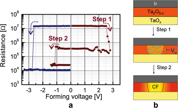
Electroforming process and filament diameter control. (a) Pulsed resistance-voltage curve of the two-step forming scheme (red) compared with the common forming scheme (blue). Small conducting filament formation is confirmed by its high resistance after step 2. (b) Schematics of the Ta2O5-δ resistive switching layer during the two-step forming process. Oxygen vacancies are generated in the Ta2O5-δ layer after step 1, and a conducting filament is formed by applying a negative pulse in step 2 [120].
Figure 12.
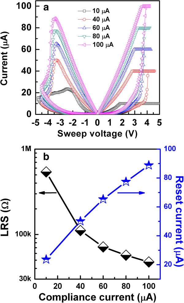
Current/voltage hysteresis with different current compliances. I-V hysteresis characteristics (a) LRS and reset currents (b) with 10- to 100-μA CCs. A device could be operated with a low reset current of 23 μA [41].
Figure 13.
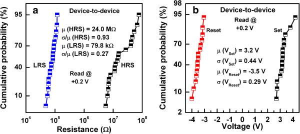
Statistical data plot. Cumulative probability plots of (a) LRS and HRS and (b) SET and RESET voltage.
Figure 14.
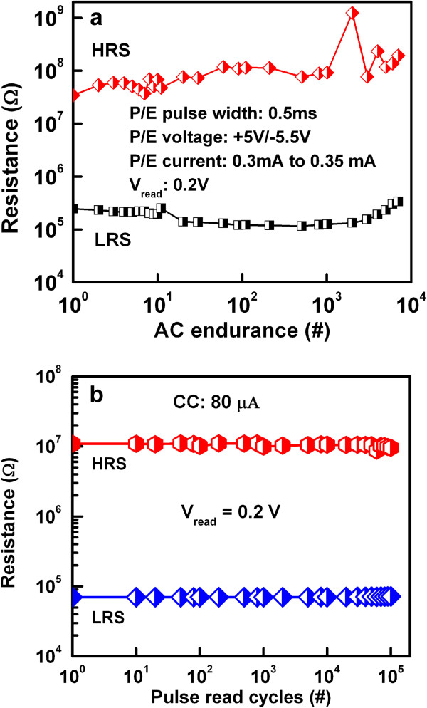
Endurance characteristics. (a) AC endurance of >104 cycles and (b) long read pulse endurance of >105 cycles at a read voltage of 0.2 V.
Figure 15.
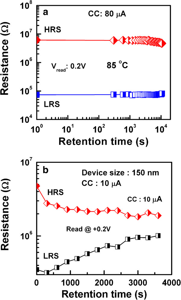
Data retention characteristics. (a) Good data retention of >104 s with a good resistance ratio of >102 at 85°C under CC of 80 μA and (b) the resistance ratio gradually decreases with retention time at a low CC of 10 μA.
Table 2.
Data comparison in published literature
| Device structure | Device size (μm 2 ) | Set/reset voltage (V) | Current compliance (μA) | Retention (s) | Resistance ratio | Endurance (cycles) |
|---|---|---|---|---|---|---|
| W/TiOx/TaOx/TiN [41] |
0.15 × 0.15 |
3.0/-3.0 |
80 |
>3 h, 85°C |
100 |
104 |
| Ir or Pt/Ta2O5-δTa2-β/Pt [109,120] |
0.5 × 0.5 |
-1/+0.8 |
80/150 |
>107 |
~10 |
109 |
| Pt/Ta2O5-x/TaO2-x/Pt [31] |
50 × 50-0.03 × 0.03 |
-2.0/+2.0 |
40-200 |
10 years, 85°C |
~10 |
1012 |
| Ru/Ta2O5/TiO2/Ru [137] |
4 × 4 |
+2.7/-1.0 |
~100 |
>106 |
~50 |
106 |
| TiN/Ti/HfOx/TiN [16,138] |
~0.4 × 0.4-0.03 × 0.03 |
1.0/-1.5 |
40, 200 |
>104, 200°C |
~100 |
108 |
| Hf, Ti, Ta/HfO2/TiN [85] |
0.04 × 0.04 |
+1.8/-3 |
100 |
>104, 200°C |
~10 |
1010 |
| TiN/Hf/HfO2/TiN [139] |
0.01 × 0.01 |
±0.5 |
<80 |
105, 200°C |
~100 |
5 × 10⁷ |
| Pt/ZrOx/HfOx/TiN [83] |
0.05 × 0.05 |
0.6/-1.5 |
50 |
105, 125°C |
~100 |
106 |
| TiN/WOx/TiN [140] | 0.06 × 0.06 | -1.4/+1.6 | 400 | 2 × 10³ h, 150°C | ~10 | 106 |
Conclusions
It is reviewed that TaOx-based bipolar resistive switching memory could be operated at a low current of 80 μA [41,109], which has prospective of RRAM applications in the future. Further, TaOx is a simple and useful material because of two stable phases of TaO2 and Ta2O5, as compared to other reported materials. Long program/erase endurance of >1010 and 10 years data retention are also reported in published literature [31,110]. So far, bilayered TaOx with inert electrodes (Pt and/or Ir) or single-layer TaOx with semi-reactive electrodes (W and Ti/W or Ta/Pt) are reported; however, conducting nano-filament formation/rupture is controlled by oxygen ion migration through bilayered or interfacial layer design under external bias. Further, high-density memory with a small size of 30 × 30 nm2 could be designed using crossbar architecture [31]. It is found that the memory performance is becoming worst at operation current of 10 μA. Therefore, it is very challenging to reduce the operation current (few microampere) of the RRAM devices. So far, good performance of TaOx-based resistive switching memory devices is investigated, as compared to other switching materials in different RRAMs. This topical review shows good prospective; however, it needs to overcome the challenges for future production of the TaOx-based nanoscale RRAM application.
Competing interests
The authors declare that they have no competing interests.
Authors’ contributions
AP and DJ reviewed the papers under the instruction of SM. AP wrote the first draft and DJ prepared Tables 1 and 2 carefully under the instruction of SM. The final draft was modified by SM. All authors read and approved the final manuscript.
Contributor Information
Amit Prakash, Email: amit.knp02@gmail.com.
Debanjan Jana, Email: debanjan.jana@gmail.com.
Siddheswar Maikap, Email: sidhu@mail.cgu.edu.tw.
Acknowledgments
This work was supported by the National Science Council (NSC), Taiwan, under contract numbers: NSC-101-2221-E-182-061 and NSC-102-2221-E-182-057-MY2. The authors thank Electronic and Optoelectronic Research Laboratories, Industrial Technology Research Institute, Hsinchu, Taiwan, for their experimental support.
References
- Hutchby J, Garner M. Assessment of the potential & maturity of selected emerging research memory technologies workshop & ERD/ERM working group meeting (April 6–7, 2010) 2010. http://www.itrs.net/Links/2010ITRS/2010Update/ToPost/ERD_ERM_2010FINALReportMemoryAssessment_ITRS.pdf.
- Keeney SN. Tech Dig - Int Electron Devices Meet2001. Washington, DC; 2001. A 130 nm generation high density Etox™ flash memory technology; pp. 2.5.1–2.5.4. [Google Scholar]
- Ray SK, Maikap S, Banerjee W, Das S. Nanocrystals for silicon based light emitting and memory devices. J Phys D Appl Phys. 2013;8:153001. doi: 10.1088/0022-3727/46/15/153001. [DOI] [Google Scholar]
- Kato Y, Yamada T, Shimada Y. 0.18-μm nondestructive readout FeRAM using charge compensation technique. IEEE Trans Electron Devices. 2005;8:2616. doi: 10.1109/TED.2005.859688. [DOI] [Google Scholar]
- Setter N, Damjanovic D, Eng L, Fox G, Gevorgian S, Hong S, Kingon A, Kohlstedt H, Park NY, Stephenson GB, Stolitchnov I, Taganstev AK, Taylor DV, Yamada T, Streiffer S. Ferroelectric thin films: review of materials, properties, and applications. J Appl Phys. 2006;8:051606. doi: 10.1063/1.2336999. [DOI] [Google Scholar]
- Durlam M, Chung Y, DeHerrera M, Engel BN, Grynkewich G, Martino B, Nguyen B, Salter J, Shah P, Slaughter JM. Proceedings of the IEEE International Conference on Integrated Circuit Design and Technology. Austin; 2007. MRAM memory for embedded and stand alone systems; pp. 1–4. [Google Scholar]
- Sekikawa M, Kiyoyama K, Hasegawa H, Miura K, Fukushima T, Ikeda S, Tanaka T, Ohno H, Koyanagi M. Tech Dig - Int Electron Devices Meet. San Francisco, CA; 2008. A novel SPRAM (SPin-transfer torque RAM)-based reconfigurable logic block for 3D-stacked reconfigurable spin processor; pp. 1–3. [Google Scholar]
- Raoux S, Burr GW, Breitwisch MJ, Rettner CT, Chen YC, Shelby RM, Salinga M, Krebs D, Chen SH, Lung HL, Lam CH. Phase-change random access memory: a scalable technology. IBM J Res Dev. 2008;8:465. [Google Scholar]
- Beck A, Bednorz JG, Gerber C, Rossel C, Widmer D. Reproducible switching effect in thin oxide films for memory applications. Appl Phys Lett. 2000;8:139. doi: 10.1063/1.126902. [DOI] [Google Scholar]
- Baek IG, Lee MS, Seo S, Lee MJ, Seo DH, Suh DS, Park JC, Park SO, Kim HS, Yoo IK, Chung UI, Moon JT. Tech Dig - Int Electron Devices Meet. San Francisco, CA; 2004. Highly scalable non-volatile resistive memory using simple binary oxide driven by asymmetric unipolar voltage pulses; pp. 587–590. [Google Scholar]
- Kozicki MN, Gopalan C, Balakrishnan M, Park M, Mitkova M. Proceedings 2004 Non-Volatile Memory Technology Symposium. Orlando; 2004. Non-volatile memory based on solid electrolytes; pp. 10–17. [Google Scholar]
- Chen A, Haddad S, Wu YC, Fang TN, Lan Z, Avanzino S, Pangrle S, Buynoski M, Rathor M, Cai W, Tripsas N, Bill C, VanBuskirk M, Taguchi M. Tech Dig - Int Electron Devices Meet. Washington, DC; 2005. Non-volatile resistive switching for advanced memory applications; pp. 746–749. [Google Scholar]
- Liu CY, Wu PH, Wang A, Jang WY, Young JC, Chiu KY, Tseng TY. Bistable resistive switching of a sputter-deposited Cr-doped SrZrO3 memory film. IEEE Electron Device Lett. 2005;8:351. [Google Scholar]
- Waser R, Aono M. Nanoionics-based resistive switching memories. Nat Mater. 2007;8:833. doi: 10.1038/nmat2023. [DOI] [PubMed] [Google Scholar]
- Sawa A. Resistive switching in transition metal oxides. Mater Today. 2008;8:28. [Google Scholar]
- Lee HY, Chen PS, Wu TY, Chen YS, Wang CC, Tzeng PJ, Lin CH, Chen F, Lien CH, Tsai MJ. Tech Dig - Int Electron Devices Meet. San Francisco, CA; 2008. Low power and high speed bipolar switching with a thin reactive Ti buffer layer in robust HfO2 based RRAM; pp. 1–4. [Google Scholar]
- Waser R, Dittmann R, Staikov G, Szot K. Redox-based resistive switching memories - nanoionic mechanisms, prospects, and challenges. Adv Mater. 2009;8:2632. doi: 10.1002/adma.200900375. [DOI] [PubMed] [Google Scholar]
- Akinaga H, Shima H. Resistive random access memory (ReRAM) based on metal oxides. Proc IEEE. 2010;8:2237. [Google Scholar]
- Pan F, Chen C, Wang ZS, Yang YC, Yang J, Zeng F. Nonvolatile resistive switching memories-characteristics, mechanisms and challenges. Proc Natl Acad Sci USA. 2010;8:1. [Google Scholar]
- Park J, Lee W, Choe M, Jung S, Son M, Kim S, Park S, Shin J, Lee D, Siddik M, Woo J, Choi G, Cha E, Lee T, Hwang H. Tech Dig - Int Electron Devices Meet. Washington, DC; 2011. Quantized conductive filament formed by limited Cu source in sub-5nm era; pp. 3.7.1–3.7.4. [Google Scholar]
- Torrezan AC, Strachan JP, Medeiros-Ribeiro G, Williams RS. Sub-nanosecond switching of a tantalum oxide memristor. Nanotechnology. 2011;8:485203. doi: 10.1088/0957-4484/22/48/485203. [DOI] [PubMed] [Google Scholar]
- Rahaman SZ, Maikap S, Tien TC, Lee HY, Chen WS, Chen FT, Kao MJ, Tsai MJ. Excellent resistive memory characteristics and switching mechanism using a Ti nanolayer at the Cu/TaOx interface. Nanoscale Res Lett. 2012;8:345. doi: 10.1186/1556-276X-7-345. [DOI] [PMC free article] [PubMed] [Google Scholar]
- Wong HSP, Lee HY, Yu S, Chen YS, Wu Y, Chen PS, Lee B, Chen FT, Tsai MJ. Metal-oxide RRAM. Proc IEEE. 1951;8:100. [Google Scholar]
- Liu Q, Sun J, Lv H, Long S, Yin K, Wan N, Li Y, Sun L, Liu M. Resistive switching: real-time observation on dynamic growth/dissolution of conductive filaments in oxide-electrolyte-based RERAM. Adv Mater. 2012;8:1774. doi: 10.1002/adma.201290080. [DOI] [PubMed] [Google Scholar]
- Yang JJ, Strukov DB, Stewart DR. Memristive devices for computing. Nat Nanotechnol. 2013;8:13. doi: 10.1038/nnano.2012.240. [DOI] [PubMed] [Google Scholar]
- International technology roadmap for semiconductors 2011 edition emerging research devices. http://www.itrs.net/Links/2011itrs/2011Tables/ERD_2011Tables.xlsx.
- Burr GW, Kurdi BN, Scott JC, Lam CH, Gopalakrishnan K, Shenoy RS. Overview of candidate device technologies for storage-class memory. IBM J Res Dev. 2008;8:449. [Google Scholar]
- Ho C-H, Hsu C-L, Chen C-C, Liu J-T, Wu C-S, Huang C-C, Hu C, Fu-Liang Y. Tech Dig - Int Electron Devices Meet. San Francisco, CA; 2010. 9 nm half-pitch functional resistive memory cell with <1 μA programming current using thermally oxidized sub-stoichiometric WOx film; pp. 19.1.1–19.1.4. [Google Scholar]
- Lee HY, Chen YS, Chen PS, Gu PY, Hsu YY, Wang SM, Liu WH, Tsai CH, Sheu SS, Chiang PC, Lin WP, Lin CH, Chen WS, Chen FT, Lien CH, Tsai MJ. Tech Dig - Int Electron Devices Meet. San Francisco, CA; 2010. Evidence and solution of over-RESET problem for HfOx based resistive memory with sub-ns switching speed and high endurance; pp. 19.7.1–19.7.4. [Google Scholar]
- Kim S, Biju KP, Jo M, Jung S, Park J, Lee J, Lee W, Shin J, Park S, Hwang H. Effect of scaling WOx-based RRAMs on their resistive switching characteristics. IEEE Electron Device Lett. 2011;8:671. [Google Scholar]
- Lee M-J, Lee CB, Lee D, Lee SR, Chang M, Hur JH, Kim Y-B, Kim C-J, Seo DH, Seo S, Chung UI, Yoo I-K, Kim K. A fast, high-endurance and scalable non-volatile memory device made from asymmetric Ta2O5-x/TaO2-x bilayer structures. Nat Mater. 2011;8:625. doi: 10.1038/nmat3070. [DOI] [PubMed] [Google Scholar]
- Hickmott TW. Low-frequency negative resistance in thin anodic oxide films. J Appl Phys. 1962;8:2669. doi: 10.1063/1.1702530. [DOI] [Google Scholar]
- Nielsen PH, Bashara NM. The reversible voltage-induced initial resistance in the negative resistance sandwich structure. IEEE Trans Electron Devices. 1964;8:243. [Google Scholar]
- Gibbons JF, Beadle WE. Switching properties of thin NiO films. Solid-State Electron. 1964;8:785. doi: 10.1016/0038-1101(64)90131-5. [DOI] [Google Scholar]
- Simmons JG, Verderber RR. New conduction and reversible memory phenomena in thin insulating films. Proc R Soc London, Ser A. 1967;8:77. doi: 10.1098/rspa.1967.0191. [DOI] [Google Scholar]
- Chua LO. Memristors-the missing circuit element. IEEE Trans Circuit Theory. 1971;8:507. [Google Scholar]
- Tsuruoka T, Terabe K, Hasegawa T, Aono M. Forming and switching mechanisms of a cation-migration-based oxide resistive memory. Nanotechnology. 2010;8:425205. doi: 10.1088/0957-4484/21/42/425205. [DOI] [PubMed] [Google Scholar]
- Chen YS, Lee HY, Chen PS, Wu TY, Wang CC, Tzeng PJ, Chen F, Tsai MJ, Lien C. An ultrathin forming-free HfOx resistance memory with excellent electrical performance. IEEE Electron Device Lett. 2010;8:1473. [Google Scholar]
- Qinan M, Zhenguo J, Junhua X. Realization of forming-free ZnO-based resistive switching memory by controlling film thickness. J Phys D Appl Phys. 2010;8:395104. doi: 10.1088/0022-3727/43/39/395104. [DOI] [Google Scholar]
- Stille S, Lenser C, Dittmann R, Koehl A, Krug I, Muenstermann R, Perlich J, Schneider CM, Klemradt U, Waser R. Detection of filament formation in forming-free resistive switching SrTiO3 devices with Ti top electrodes. Appl Phys Lett. 2012;8:223503. doi: 10.1063/1.4724108. [DOI] [Google Scholar]
- Prakash A, Maikap S, Chiu H-C, Tien T-C, Lai C-S. Enhanced resistive switching memory characteristics and mechanism using a Ti nanolayer at the W/TaOx interface. Nanoscale Res Lett. 2013;8:288. doi: 10.1186/1556-276X-8-288. [DOI] [PMC free article] [PubMed] [Google Scholar]
- Akinaga H, Shima H, Takano F, Inoue IH, Takagi H. Resistive switching effect in metal/insulator/metal heterostructures and its application for non-volatile memory. IEEJ T Electr. 2007;8:453. [Google Scholar]
- Szot K, Speier W, Bihlmayer G, Waser R. Switching the electrical resistance of individual dislocations in single-crystalline SrTiO3. Nat Mater. 2006;8:312. doi: 10.1038/nmat1614. [DOI] [PubMed] [Google Scholar]
- Kwon D-H, Kim KM, Jang JH, Jeon JM, Lee MH, Kim GH, Li X-S, Park G-S, Lee B, Han S, Kim M, Hwang CS. Atomic structure of conducting nanofilaments in TiO2 resistive switching memory. Nat Nanotechnol. 2010;8:148. doi: 10.1038/nnano.2009.456. [DOI] [PubMed] [Google Scholar]
- Xu Z, Bando Y, Wang W, Bai X, Golberg D. Real-time in situ HRTEM-resolved resistance switching of Ag2S nanoscale ionic conductor. ACS Nano. 2010;8:2515. doi: 10.1021/nn100483a. [DOI] [PubMed] [Google Scholar]
- Rahaman SZ, Maikap S, Chen WS, Lee HY, Chen FT, Tien TC, Tsai MJ. Impact of TaOx nanolayer at the GeSex/W interface on resistive switching memory performance and investigation of Cu nanofilament. J Appl Phys. 2012;8:063710. doi: 10.1063/1.3696972. [DOI] [Google Scholar]
- Yang Y, Gao P, Gaba S, Chang T, Pan X, Lu W. Observation of conducting filament growth in nanoscale resistive memories. Nat Commun. 2012;8:732. doi: 10.1038/ncomms1737. [DOI] [PubMed] [Google Scholar]
- Rahaman SZ, Maikap S, Chen WS, Lee HY, Chen FT, Kao MJ, Tsai MJ. Repeatable unipolar/bipolar resistive memory characteristics and switching mechanism using a Cu nanofilament in a GeOx film. Appl Phys Lett. 2012;8:073106. doi: 10.1063/1.4745783. [DOI] [PMC free article] [PubMed] [Google Scholar]
- Jeong HY, Lee JY, Ryu M-K, Choi S-Y. Bipolar resistive switching in amorphous titanium oxide thin film. Phys Status Solidi RRL. 2010;8:28. doi: 10.1002/pssr.200903383. [DOI] [Google Scholar]
- Tsui S, Baikalov A, Cmaidalka J, Sun YY, Wang YQ, Xue YY, Chu CW, Chen L, Jacobson AJ. Field-induced resistive switching in metal-oxide interfaces. Appl Phys Lett. 2004;8:317. doi: 10.1063/1.1768305. [DOI] [Google Scholar]
- Jeon SH, Park BH, Lee J, Lee B, Han S. First-principles modeling of resistance switching in perovskite oxide material. Appl Phys Lett. 2006;8:042904. doi: 10.1063/1.2234840. [DOI] [Google Scholar]
- Seong D-j, Jo M, Lee D, Hwang H. HPHA effect on reversible resistive switching of P/Nb -doped SrTiO3 Schottky junction for nonvolatile memory application. Electrochem Solid-State Lett. 2007;8:H168. doi: 10.1149/1.2718396. [DOI] [Google Scholar]
- Nian YB, Strozier J, Wu NJ, Chen X, Ignatiev A. Evidence for an oxygen diffusion model for the electric pulse induced resistance change effect in transition-metal oxides. Phys Rev Lett. 2007;8:146403. doi: 10.1103/PhysRevLett.98.146403. [DOI] [PubMed] [Google Scholar]
- Sawa A, Fujii T, Kawasaki M, Tokura Y. Hysteretic current–voltage characteristics and resistance switching at a rectifying Ti/Pr0.7Ca0.3MnO3 interface. Appl Phys Lett. 2004;8:4073. doi: 10.1063/1.1812580. [DOI] [Google Scholar]
- Fujii T, Kawasaki M, Sawa A, Akoh H, Kawazoe Y, Tokura Y. Hysteretic current–voltage characteristics and resistance switching at an epitaxial oxide Schottky junction SrRuO3/SrTi0.99Nb0.01O3. Appl Phys Lett. 2005;8:012107. doi: 10.1063/1.1845598. [DOI] [Google Scholar]
- Rozenberg MJ, Inoue IH, Sánchez MJ. Nonvolatile memory with multilevel switching: a basic model. Phys Rev Lett. 2004;8:178302. doi: 10.1103/PhysRevLett.92.178302. [DOI] [PubMed] [Google Scholar]
- Fors R, Khartsev SI, Grishin AM. Giant resistance switching in metal-insulator-manganite junctions: evidence for Mott transition. Phys Rev B. 2005;8:045305. [Google Scholar]
- Oka T, Nagaosa N. Interfaces of correlated electron systems: proposed mechanism for colossal electroresistance. Phys Rev Lett. 2005;8:266403. doi: 10.1103/PhysRevLett.95.266403. [DOI] [PubMed] [Google Scholar]
- Kund M, Beitel G, Pinnow CU, Röhr T, Schumann J, Symanczyk R, Ufert KD, Müller G. Tech Dig - Int Electron Devices Meet. Washington, DC; 2005. Conductive bridging RAM (CBRAM): an emerging non-volatile memory technology scalable to sub 20 nm; pp. 754–757. [Google Scholar]
- Rahaman SZ, Maikap S, Das A, Prakash A, Wu YH, Lai CS, Tien TC, Chen WS, Lee HY, Chen FT, Tsai MJ, Chang LB. Enhanced nanoscale resistive switching memory characteristics and switching mechanism using high-Ge-content Ge0.5Se0.5 solid electrolyte. Nanoscale Res Lett. 2012;8:614. doi: 10.1186/1556-276X-7-614. [DOI] [PMC free article] [PubMed] [Google Scholar]
- Kozicki MN, Balakrishnan M, Gopalan C, Ratnakumar C, Mitkova M. 2005 Non-Volatile Memory Technology Symposium. Dallas, TX; 2005. Programmable metallization cell memory based on Ag-Ge-S and Cu-Ge-S solid electrolytes; p. 83. [Google Scholar]
- Jameson JR, Gilbert N, Koushan F, Saenz J, Wang J, Hollmer S, Kozicki M, Derhacobian N. Quantized conductance in Ag/GeS2/W conductive-bridge memory cells. IEEE Electron Device Lett. 2012;8:257. [Google Scholar]
- Kaeriyama S, Sakamoto T, Sunamura H, Mizuno M, Kawaura H, Hasegawa T, Terabe K, Nakayama T, Aono M. A nonvolatile programmable solid-electrolyte nanometer switch. IEEE J Solid-State Circuits. 2005;8:168. [Google Scholar]
- Terabe K, Hasegawa T, Nakayama T, Aono M. Quantized conductance atomic switch. Nature. 2005;8:47. doi: 10.1038/nature03190. [DOI] [PubMed] [Google Scholar]
- Sakamoto T, Lister K, Banno N, Hasegawa T, Terabe K, Aono M. Electronic transport in Ta2O5 resistive switch. Appl Phys Lett. 2007;8:092110. doi: 10.1063/1.2777170. [DOI] [Google Scholar]
- Maikap S, Rahaman SZ, Wu TY, Chen FT, Kao MJ, Tsai MJ. The 39th European Solid-State Device Research Conference and the 35th European Solid-state Circuits Conference (ESSDERC/ESSCIRC) Athens; 2009. Low current (5 pA) resistive switching memory using high-κ Ta2O5 solid electrolyte; p. 217. [Google Scholar]
- Schindler C, Thermadam SCP, Waser R, Kozicki MN. Bipolar and unipolar resistive switching in Cu-doped SiO2. IEEE Trans Electron Devices. 2007;8:2762. [Google Scholar]
- Hsiung CP, Liao HW, Gan JY, Wu TB, Hwang JC, Chen F, Tsai MJ. Formation and instability of silver nanofilament in Ag-based programmable metallization cells. ACS Nano. 2010;8:5414. doi: 10.1021/nn1010667. [DOI] [PubMed] [Google Scholar]
- Liu Q, Long S, Lv H, Wang W, Niu J, Huo Z, Chen J, Liu M. Controllable growth of nanoscale conductive filaments in solid-electrolyte-based ReRAM by using a metal nanocrystal covered bottom electrode. ACS Nano. 2010;8:6162. doi: 10.1021/nn1017582. [DOI] [PubMed] [Google Scholar]
- Nagata T, Haemori M, Yamashita Y, Yoshikawa H, Iwashita Y, Kobayashi K, Chikyow T. Bias application hard X-ray photoelectron spectroscopy study of forming process of Cu/HfO2/Pt resistive random access memory structure. Appl Phys Lett. 2011;8:223517. doi: 10.1063/1.3664781. [DOI] [Google Scholar]
- Yoon J, Choi H, Lee D, Park JB, Lee J, Seong DJ, Ju Y, Chang M, Jung S, Hwang H. Excellent switching uniformity of Cu-doped MoOx/GdOx bilayer for nonvolatile memory applications. IEEE Electron Device Lett. 2009;8:457. [Google Scholar]
- Tada M, Sakamoto T, Banno N, Aono M, Hada H, Kasai N. Nonvolatile crossbar switch using TiOx/TaSiOy solid electrolyte. IEEE Trans Electron Devices. 1987;8:57. [Google Scholar]
- Goux L, Opsomer K, Degraeve R, Muller R, Detavernier C, Wouters DJ, Jurczak M, Altimime L, Kittl JA. Influence of the Cu-Te composition and microstructure on the resistive switching of Cu-Te/Al2O3/Si cells. Appl Phys Lett. 2011;8:053502. doi: 10.1063/1.3621835. [DOI] [Google Scholar]
- Kim DC, Seo S, Ahn SE, Suh DS, Lee MJ, Park BH, Yoo IK, Baek IG, Kim HJ, Yim EK, Lee JE, Park SO, Kim HS, Chung UI, Moon JT, Ryu BI. Electrical observations of filamentary conductions for the resistive memory switching in NiO films. Appl Phys Lett. 2006;8:202102. doi: 10.1063/1.2204649. [DOI] [Google Scholar]
- Ielmini D, Nardi F, Cagli C. Physical models of size-dependent nanofilament formation and rupture in NiO resistive switching memories. Nanotechnology. 2011;8:254022. doi: 10.1088/0957-4484/22/25/254022. [DOI] [PubMed] [Google Scholar]
- Jousseaume V, Fantini A, Nodin JF, Guedj C, Persico A, Buckley J, Tirano S, Lorenzi P, Vignon R, Feldis H, Minoret S, Grampeix H, Roule A, Favier S, Martinez E, Calka P, Rochat N, Auvert G, Barnes JP, Gonon P, Vallée C, Perniola L, De Salvo B. Comparative study of non-polar switching behaviors of NiO- and HfO2-based oxide resistive-RAMs. Solid-State Electron. 2011;8:62. doi: 10.1016/j.sse.2010.11.023. [DOI] [Google Scholar]
- Yang JJ, Pickett MD, Li X, Ohlberg DAA, Stewart DR, Williams RS. Memristive switching mechanism for metal/oxide/metal nanodevices. Nat Nanotechnol. 2008;8:429. doi: 10.1038/nnano.2008.160. [DOI] [PubMed] [Google Scholar]
- Hermes C, Bruchhaus R, Waser R. Forming-free TiO2-based resistive switching devices on CMOS-compatible W-plugs. IEEE Electron Device Lett. 2011;8:1588. [Google Scholar]
- Park J, Biju KP, Jung S, Lee W, Lee J, Kim S, Park S, Shin J, Hwang H. Multibit operation of TiOx-based ReRAM by Schottky barrier height engineering. IEEE Electron Device Lett. 2011;8:476. [Google Scholar]
- Cheng CH, Chen PC, Wu YH, Yeh FS, Chin A. Long-endurance nanocrystal TiO2 resistive memory using a TaON buffer layer. IEEE Electron Device Lett. 2011;8:1749. [Google Scholar]
- Park WY, Kim GH, Seok JY, Kim KM, Song SJ, Lee MH, Hwang CS. A Pt/TiO2/Ti Schottky-type selection diode for alleviating the sneak current in resistance switching memory arrays. Nanotechnology. 2010;8:195201. doi: 10.1088/0957-4484/21/19/195201. [DOI] [PubMed] [Google Scholar]
- Lee H-Y, Chen P-S, Wang C-C, Maikap S, Tzeng P-J, Lin C-H, Lee L-S, Tsai M-J. Low-power switching of nonvolatile resistive memory using hafnium oxide. Jpn J Appl Phys, Part 1. 2007;8:2175. doi: 10.1143/JJAP.46.2175. [DOI] [Google Scholar]
- Lee J, Bourim EM, Lee W, Park J, Jo M, Jung S, Shin J, Hwang H. Effect of ZrOx/HfOx bilayer structure on switching uniformity and reliability in nonvolatile memory applications. Appl Phys Lett. 2010;8:172105. doi: 10.1063/1.3491803. [DOI] [Google Scholar]
- Walczyk D, Walczyk C, Schroeder T, Bertaud T, Sowinska M, Lukosius M, Fraschke M, Tillack B, Wenger C. Resistive switching characteristics of CMOS embedded HfO2-based 1T1R cells. Microelectron Eng. 2011;8:1133. doi: 10.1016/j.mee.2011.03.123. [DOI] [Google Scholar]
- Chen YY, Goux L, Clima S, Govoreanu B, Degraeve R, Kar GS, Fantini A, Groeseneken G, Wouters DJ, Jurczak M. Endurance/retention trade-off on HfO2/metal cap 1T1R bipolar RRAM. IEEE Trans Electron Devices. 2013;8:1114. [Google Scholar]
- Yu S, Chen H-Y, Gao B, Kang J, Wong HSP. HfOx-based vertical resistive switching random access memory suitable for bit-cost-effective three-dimensional cross-point architecture. ACS Nano. 2013;8:2320. doi: 10.1021/nn305510u. [DOI] [PubMed] [Google Scholar]
- Chen A, Haddad S, Wu YC, Fang TN, Kaza S, Lan Z. Erasing characteristics of Cu2O metal-insulator-metal resistive switching memory. Appl Phys Lett. 2008;8:013503. doi: 10.1063/1.2828864. [DOI] [Google Scholar]
- Sun X, Li G, Chen L, Shi Z, Zhang W. Bipolar resistance switching characteristics with opposite polarity of Au/SrTiO3/Ti memory cells. Nanoscale Res Lett. 2011;8:1. doi: 10.1186/1556-276X-6-599. [DOI] [PMC free article] [PubMed] [Google Scholar]
- Lin CY, Wu CY, Wu CYC-Y, Lee TC, Yang FL, Hu C, Tseng TY. Effect of top electrode material on resistive switching properties of ZrO2 film memory devices. IEEE Electron Device Lett. 2007;8:366. [Google Scholar]
- Liu Q, Long S, Wang W, Zuo Q, Zhang S, Chen J, Liu M. Improvement of resistive switching properties in ZrO2-based ReRAM with implanted Ti ions. IEEE Electron Device Lett. 2009;8:1335. [Google Scholar]
- Wang S-Y, Lee D-Y, Tseng T-Y, Lin C-Y. Effects of Ti top electrode thickness on the resistive switching behaviors of rf-sputtered ZrO2 memory films. Appl Phys Lett. 2009;8:112904. doi: 10.1063/1.3231872. [DOI] [Google Scholar]
- Wang SY, Lee DY, Huang TY, Wu JW, Tseng TY. Controllable oxygen vacancies to enhance resistive switching performance in a ZrO2-based RRAM with embedded Mo layer. Nanotechnology. 2010;8:495201. doi: 10.1088/0957-4484/21/49/495201. [DOI] [PubMed] [Google Scholar]
- Chien WC, Chen YC, Lai EK, Yao YD, Lin P, Horng SF, Gong J, Chou TH, Lin HM, Chang MN, Shih YH, Hsieh KY, Liu R, Chih-Yuan L. Unipolar switching behaviors of RTO WOx RRAM. IEEE Electron Device Lett. 2010;8:126. [Google Scholar]
- Lin CY, Wu CY, Hu C, Tseng TY. Bistable resistive switching in Al2O3 memory thin films. J Electrochem Soc. 2007;8:G189. doi: 10.1149/1.2750450. [DOI] [Google Scholar]
- Banerjee W, Rahaman SZ, Prakash A, Maikap S. High-κ Al2O3/WOx bilayer dielectrics for low-power resistive switching memory applications. Jpn J Appl Phys. 2011;8:10PH01. doi: 10.1143/JJAP.50.10PH01. [DOI] [Google Scholar]
- Wu Y, Yu S, Lee B, Wong HSP. Low-power TiN/Al2O3/Pt resistive switching device with sub-20 μA switching current and gradual resistance modulation. J Appl Phys. 2011;8:094104. doi: 10.1063/1.3657938. [DOI] [Google Scholar]
- Banerjee W, Maikap S, Rahaman SZ, Prakash A, Tien TC, Li WC, Yang JR. Improved resistive switching memory characteristics using core-shell IrOx nano-dots in Al2O3/WOx bilayer structure. J Electrochem Soc. 2012;8:H177. doi: 10.1149/2.067202jes. [DOI] [Google Scholar]
- Peng HY, Li GP, Ye JY, Wei ZP, Zhang Z, Wang DD, Xing GZ, Wu T. Electrode dependence of resistive switching in Mn-doped ZnO: filamentary versus interfacial mechanisms. Appl Phys Lett. 2010;8:192113. doi: 10.1063/1.3428365. [DOI] [Google Scholar]
- Andy S, Wendi Z, Julia Q, Han-Jen Y, Shuyi C, Zetian M, Ishiang S. Highly stable resistive switching on monocrystalline ZnO. Nanotechnology. 2010;8:125201. doi: 10.1088/0957-4484/21/12/125201. [DOI] [PubMed] [Google Scholar]
- Chiu FC, Li PW, Chang WY. Reliability characteristics and conduction mechanisms in resistive switching memory devices using ZnO thin films. Nanoscale Res Lett. 2012;8:1. doi: 10.1186/1556-276X-7-1. [DOI] [PMC free article] [PubMed] [Google Scholar]
- Peng CN, Wang CW, Chan TC, Chang WY, Wang YC, Tsai HW, Wu WW, Chen LJ, Chueh YL. Resistive switching of Au/ZnO/Au resistive memory: an in situ observation of conductive bridge formation. Nanoscale Res Lett. 2012;8:1. doi: 10.1186/1556-276X-7-1. [DOI] [PMC free article] [PubMed] [Google Scholar]
- Yao J, Zhong L, Natelson D, Tour JM. Intrinsic resistive switching and memory effects in silicon oxide. Appl Phys A. 2011;8:835. doi: 10.1007/s00339-011-6267-6. [DOI] [Google Scholar]
- Mehonic A, Cueff S, Wojdak M, Hudziak S, Jambois O, Labbe C, Garrido B, Rizk R, Kenyon AJ. Resistive switching in silicon suboxide films. J Appl Phys. 2012;8:074507. doi: 10.1063/1.3701581. [DOI] [Google Scholar]
- Cao X, Li X, Gao X, Yu W, Liu X, Zhang Y, Chen L, Cheng X. Forming-free colossal resistive switching effect in rare-earth-oxide Gd2O3 films for memristor applications. J Appl Phys. 2009;8:073723. doi: 10.1063/1.3236573. [DOI] [Google Scholar]
- Jana D, Maikap S, Tien TC, Lee HY, Chen WS, Chen FT, Kao MJ, Tsai MJ. Formation-polarity-dependent improved resistive switching memory performance using IrOx/GdOx/WOx/W structure. Jpn J Appl Phys. 2012;8:04DD17. doi: 10.1186/1556-276X-7-194. [DOI] [PMC free article] [PubMed] [Google Scholar]
- Seong DJ, Hassan M, Choi H, Lee J, Yoon J, Park JB, Lee W, Oh MS, Hwang H. Resistive-switching characteristics of Al/Pr0.7Ca0.3MnO3 for nonvolatile memory applications. IEEE Electron Device Lett. 2009;8:919. [Google Scholar]
- Cheng CH, Chin A, Yeh FS. Ultralow switching energy Ni/GeOx/HfON/TaN RRAM. IEEE Electron Device Lett. 2011;8:366. [Google Scholar]
- Prakash A, Maikap S, Rahaman S, Majumdar S, Manna S, Ray S. Resistive switching memory characteristics of Ge/GeOx nanowires and evidence of oxygen ion migration. Nanoscale Res Lett. 2013;8:220. doi: 10.1186/1556-276X-8-220. [DOI] [PMC free article] [PubMed] [Google Scholar]
- Wei Z, Kanzawa Y, Arita K, Katoh Y, Kawai K, Muraoka S, Mitani S, Fujii S, Katayama K, Iijima M, Mikawa T, Ninomiya T, Miyanaga R, Kawashima Y, Tsuji K, Himeno A, Okada T, Azuma R, Shimakawa K, Sugaya H, Takagi T, Yasuhara R, Khoriba G, Kumigashira H, Oshima M. Tech Dig - Int Electron Devices Meet. San Francisco, CA; 2008. Highly reliable TaOx ReRAM and direct evidence of redox reaction mechanism; pp. 1–4. [Google Scholar]
- Yang JJ, Zhang MX, Strachan JP, Miao F, Pickett MD, Kelley RD, Medeiros-Ribeiro G, Williams RS. High switching endurance in TaOx memristive devices. Appl Phys Lett. 2010;8:232102. doi: 10.1063/1.3524521. [DOI] [Google Scholar]
- Zhang L, Huang R, Zhu M, Qin S, Kuang Y, Gao D, Shi C, Wang Y. Unipolar TaOx-based resistive change memory realized with electrode engineering. IEEE Electron Device Lett. 2010;8:966. [Google Scholar]
- Gu T, Tada T, Watanabe S. Conductive path formation in the Ta2O5 atomic switch: first-principles analyses. ACS Nano. 2010;8:6477. doi: 10.1021/nn101410s. [DOI] [PubMed] [Google Scholar]
- Wei Z, Takagi T, Kanzawa Y, Katoh Y, Ninomiya T, Kawai K, Muraoka S, Mitani S, Katayama K, Fujii S, Miyanaga R, Kawashima Y, Mikawa T, Shimakawa K, Aono K. Tech Dig - Int Electron Devices Meet. Washington, DC; 2011. Demonstration of high-density ReRAM ensuring 10-year retention at 85°C based on a newly developed reliability model; pp. 31.4.1–31.4.4. [Google Scholar]
- Prakash A, Maikap S, Lai CS, Tien TC, Chen WS, Lee HY, Chen FT, Kao MJ, Tsai MJ. Bipolar resistive switching memory using bilayer TaOx/WOx films. Solid-State Electron. 2012;8:35. [Google Scholar]
- Chen C, Song C, Yang J, Zeng F, Pan F. Oxygen migration induced resistive switching effect and its thermal stability in W/TaOx/Pt structure. Appl Phys Lett. 2012;8:253509. doi: 10.1063/1.4730601. [DOI] [Google Scholar]
- Prakash A, Maikap S, Lai CS, Lee HY, Chen WS, Chen FT, Kao MJ, Tsai MJ. Improvement of uniformity of resistive switching parameters by selecting the electroformation polarity in IrOx/TaOx/WOx/W structure. Jpn J Appl Phys, Part 1. 2012;8:04DD06. [Google Scholar]
- Yang Y, Sheridan P, Lu W. Complementary resistive switching in tantalum oxide-based resistive memory devices. Appl Phys Lett. 2012;8:203112. doi: 10.1063/1.4719198. [DOI] [Google Scholar]
- Bishop SM, Bakhru H, Capulong JO, Cady NC. Influence of the SET current on the resistive switching properties of tantalum oxide created by oxygen implantation. Appl Phys Lett. 2012;8:142111. doi: 10.1063/1.3701154. [DOI] [Google Scholar]
- Marinella MJ, Dalton SM, Mickel PR, Dodd PED, Shaneyfelt MR, Bielejec E, Vizkelethy G, Kotula PG. Initial assessment of the effects of radiation on the electrical characteristics of TaOx memristive memories. IEEE Trans Nucl Sci. 2012;8:2987. [Google Scholar]
- Ninomiya T, Wei Z, Muraoka S, Yasuhara R, Katayama K, Takagi T. Conductive filament scaling of TaOx bipolar ReRAM for improving data retention under low operation current. IEEE Trans Electron Devices. 2013;8:1384. [Google Scholar]
- Diokh T, Le-Roux E, Jeannot S, Cagli C, Jousseaume V, Nodin J-F, Gros-Jean M, Gaumer C, Mellier M, Cluzel J, Carabasse C, Candelier P, De Salvo B. Study of resistive random access memory based on TiN/TaOx/TiN integrated into a 65 nm advanced complementary metal oxide semiconductor technology. Thin Solid Films. 2013;8:24. [Google Scholar]
- Mickel PR, Lohn AJ, Choi BJ, Yang JJ, Zhang M-X, Marinella MJ, James CD, Williams RS. A physical model of switching dynamics in tantalum oxide memristive devices. Appl Phys Lett. 2013;8:223502. doi: 10.1063/1.4809530. [DOI] [Google Scholar]
- Schmelzer S, Linn E, Bottger U, Waser R. Uniform complementary resistive switching in tantalum oxide using current sweeps. IEEE Electron Device Lett. 2013;8:114. [Google Scholar]
- Lee D, Woo J, Cha E, Kim S, Lee W, Park S, Hwang H. Interface engineering for low power and uniform resistive switching in bi-layer structural filament type ReRAM. Microelectron Eng. 2013;8:385. [Google Scholar]
- Kim S, Kim S-J, Kim KM, Lee SR, Chang M, Cho E, Kim Y-B, Kim CJ, In Chung U. Physical electro-thermal model of resistive switching in bi-layered resistance-change memory. Sci Rep. 2013;8:1. doi: 10.1038/srep01680. [DOI] [PMC free article] [PubMed] [Google Scholar]
- Zhuo VYQ, Jiang Y, Li MH, Chua EK, Zhang Z, Pan JS, Zhao R, Shi LP, Chong TC, Robertson J. Band alignment between Ta2O5 and metals for resistive random access memory electrodes engineering. Appl Phys Lett. 2013;8:062106. doi: 10.1063/1.4792274. [DOI] [Google Scholar]
- Elliman RG, Saleh MS, Kim TH, Venkatachalam DK, Belay K, Ruffell S, Kurunczi P, England J. Application of ion-implantation for improved non-volatile resistive random access memory (ReRAM) Nucl Instrum Methods Phys Res, Sect B. 2013;8:98. [Google Scholar]
- Yang Y, Choi S, Lu W. Oxide heterostructure resistive memory. Nano Lett. 2013;8:2908. doi: 10.1021/nl401287w. [DOI] [PubMed] [Google Scholar]
- Garg SP, Krishnamurthy N, Awasthi A, Venkatraman M. The O-Ta (oxygen-tantalum) system. J Phase Equil. 1996;8:63. doi: 10.1007/BF02648373. [DOI] [Google Scholar]
- Birks N, Meier GH, Pettit FS. Introduction to the high-temperature oxidation of metals. Cambridge: Cambridge University Press; 2006. http://www.doitpoms.ac.uk/tlplib/ellingham_diagrams/interactive.php. [Google Scholar]
- Fujimoto M, Koyama H, Konagai M, Hosoi Y, Ishihara K, Ohnishi S, Awaya N. TiO2 anatase nanolayer on TiN thin film exhibiting high-speed bipolar resistive switching. Appl Phys Lett. 2006;8:223509. doi: 10.1063/1.2397006. [DOI] [Google Scholar]
- Hur JH, Lee M-J, Lee CB, Kim Y-B, Kim C-J. Modeling for bipolar resistive memory switching in transition-metal oxides. Phys Rev B. 2010;8:155321. [Google Scholar]
- Yoshida C, Kinoshita K, Yamasaki T, Sugiyama Y. Direct observation of oxygen movement during resistance switching in NiO/Pt film. Appl Phys Lett. 2008;8:042106. doi: 10.1063/1.2966141. [DOI] [Google Scholar]
- Linn E, Rosezin R, Kugeler C, Waser R. Complementary resistive switches for passive nanocrossbar memories. Nat Mater. 2010;8:403. doi: 10.1038/nmat2748. [DOI] [PubMed] [Google Scholar]
- Long S, Lian X, Cagli C, Cartoix X, Rurali R, Miranda E, Jimenez D, Perniola L, Ming Liu M, Sune J. Quantum-size effects in hafnium-oxide resistive switching. Appl Phys Lett. 2013;8:183505. doi: 10.1063/1.4802265. [DOI] [Google Scholar]
- Long S, Cagli C, Ielmini D, Liu M, Sune J. Analysis and modeling of resistive switching statistics. J Appl Phys. 2012;8:074508. doi: 10.1063/1.3699369. [DOI] [Google Scholar]
- Terai M, Sakotsubo Y, Saito Y, Kotsuji S, Hada H. Tech Dig - Int Electron Devices Meet. Baltimore, MD; 2009. Effect of bottom electrode of ReRAM with Ta2O5/TiO2 stack on RTN and retention; pp. 1–4. [Google Scholar]
- Chen YS, Lee HY, Chen PS, Liu WH, Wang SM, Gu PY, Hsu YY, Tsai CH, Chen WS, Chen F, Tsai MJ, Lien C. Robust high-resistance state and improved endurance of HfOx resistive memory by suppression of current overshoot. IEEE Electron Device Lett. 2011;8:1585. [Google Scholar]
- Govoreanu B, Kar GS, Chen Y, Paraschiv V, Kubicek S, Fantini A, Radu IP, Goux L, Clima S, Degraeve R, Jossart N, Richard O, Vandeweyer T, Seo K, Hendrickx P, Pourtois G, Bender H, Altimime L, Wouters DJ, Kittl JA, Jurczak M. Tech Dig - Int Electron Devices Meet. Washington, DC; 2011. 10 × 10nm2 Hf/HfOx crossbar resistive RAM with excellent performance, reliability and low-energy operation; pp. 31.6.1–31.6.4. [Google Scholar]
- Chien WC, Chen YR, Chen YC, Chuang ATH, Lee FM, Lin YY, Lai EK, Shih YH, Hsieh KY, Chih-Yuan L. Tech Dig - Int Electron Devices Meet. San Francisco, CA; 2010. A forming-free WOx resistive memory using a novel self-aligned field enhancement feature with excellent reliability and scalability; pp. 19.2.1–19.2.4. [Google Scholar]


