Abstract
Understanding the grain size-dependent failure behavior of polycrystalline graphene is important for its applications both structurally and functionally. Here we perform molecular dynamics simulations to study the failure behavior of polycrystalline graphene by varying both grain size and distribution. We show that polycrystalline graphene fails in a brittle mode and grain boundary junctions serve as the crack nucleation sites. We also show that its breaking strength and average grain size follow an inverse pseudo Hall-Petch relation, in agreement with experimental measurements. Further, we find that this inverse pseudo Hall-Petch relation can be naturally rationalized by the weakest-link model, which describes the failure behavior of brittle materials. Our present work reveals insights into controlling the mechanical properties of polycrystalline graphene and provides guidelines for the applications of polycrystalline graphene in flexible electronics and nano-electronic-mechanical devices.
The outstanding mechanical properties of pristine graphene, such as an extremely high Young's modulus of around 1 TPa and a high breaking strength of 130 GPa1, along with its spectacular electronic and thermal properties2,3, make it a promising material for a wide range of applications in flexible electronics and nano-electronic-mechanical systems4,5,6,7,8. However, it is still a daunting challenge to fabricate large sheets of pristine single-crystalline graphene. So far, large-area, monolayer graphene produced by chemical vapor deposition (CVD) is polycrystalline in nature and thus contains internal grain boundaries (GBs)9,10,11,12,13. It is well-known that the properties of bulk polycrystalline materials are often dictated by the size of their grains and by the type of their GBs. Several groups have carried out experiments and modeling on polycrystalline graphene and reported the correlations between the grain size and mechanical properties, including the failure strain, the breaking strength, and the Young's modulus14,15,16,17,18,19,20,21. However, the conclusions drawn from these studies are often inconsistent. Some studies15,18 showed that GBs severely weaken the breaking strength of polycrystalline graphene, while other studies, for example, Lee et al.17 and Rasool et al.22 reported that its strength is only slightly reduced despite the presence of GBs. Undoubtedly, the understanding of grain size-dependent failure behavior of polycrystalline graphene is not only essential to control its mechanical properties, but also conducive for its applications in flexible electronics and nano-electronic-mechanical devices.
In this paper, we perform a series of MD simulations to investigate the mechanical properties of polycrystalline graphene under tensile loading by varying both grain size and distribution. More specifically, we would like to answer the following questions: (1) What are the correlations between the average grain size and mechanical properties of polycrystalline graphene, such as failure strain, breaking strength, and Young's modulus? (2) How does the distribution of grain size affect the strength? (3) What type of defect controls the breaking strength and the failure pattern for polycrystalline graphene? Our present investigation reveals that the failure strength of polycrystalline graphene follows an inverse pseudo Hall-Petch relation and GB junctions controls the breaking strength of polycrystalline graphene. Furthermore, a specific type of GB junction is found to be highly prone to crack nucleation in polycrystalline graphene, where one of its connecting GBs is perpendicular or nearly perpendicular to the loading direction. Crack preferentially starts at this specific type of GB junction, and then initially propagates along this GB and further branches out along other connected GBs and/or across grain interior, causing its ultimate failure.
Results
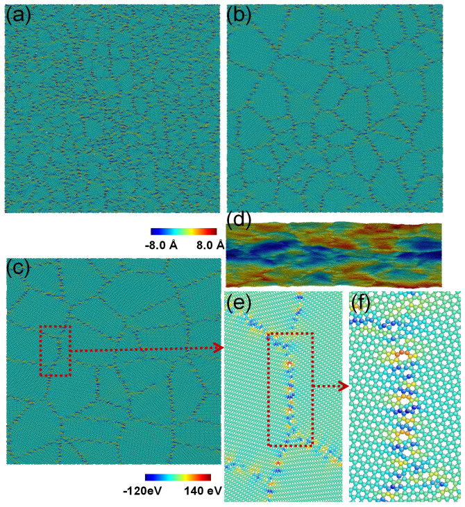
Figure 1(a–c) show the top views of typical microstructures of annealed polycrystalline graphene with an average grain size of 3, 7 and 11 nm, respectively. Atoms are colored according to their atomic stress level. Figure 1(d) displays the side view of the annealed polycrystalline graphene with average grain size of 11 nm, in which the atoms are colored according to their out-of-plane displacement. These out-of-plane deflections are known to help minimize the energy of membrane-like crystalline structures23,24. Figure 1(e–f) depict the close-up views of GBs and junctions, which are composed of large fractions of pentagons and heptagons, and also small factions of squares, octagons, and vacancies. Our atomistic model for generating polycrystalline graphene follows Kotakoski et al.16 and Zhang et al.25 in which GBs were generated through a random process. A quantitative measure of the probabilities for the presence of squares, pentagons, heptagons, and octagons in polycrystalline graphene was reported by Kotakoski et al.16. The GB structures generated by this model exhibit a slightly higher degree of disorder, typical for polycrystalline graphene grown by CVD12,26, and are consistent with previous MD simulations16,25,26,27 and experimental observations12,26.
Figure 1. The atomic configurations of the annealed polycrystalline graphene.
(a–c) Top view of a 50 nm × 50 nm annealed polycrystalline graphene sheet with average grain size of 3, 7, and 11 nm, respectively. Atoms are colored according to their atomic stresses. (d) Side view of the annealed polycrystalline graphene with average grain size of 11 nm. Atoms are colored according to their out-of-plane displacement. (e–f) The close-up views of GBs and junctions. Atoms are colored according to their atomic stresses.
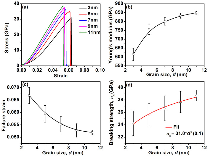
The tensile stress-strain curves for polycrystalline graphene with an average grain size of 3, 5, 7, 9, and 11 nm are plotted in Fig. 2(a). Initially the gradient of the stress-strain curves increases as the applied strain increases, in agreement with the previous MD simulation results19,25. This gradient increment is a characteristic of the entropic elastic behavior arising from erasing the wrinkle in a thin membrane structure25. As the applied strain is increased further, the polycrystalline graphene gradually flattens under stretching, the sp2 C–C bonds are directly stretched and as a result, the stress becomes linearly dependent on the applied strain. The slope of the stress-strain curve in this range gives the Young's modulus. Finally the polycrystalline graphene fails due to crack nucleation and propagation. The trends of the Young's modulus, the failure strain, and the breaking strength taken as the peak tensile stress, as a function of the average grain size are plotted in Fig. 2(b–d), respectively. For each selected value of the average grain size, we perform simulations on 5 randomly generated samples with the same average grain size but different initial grain configurations, and use the average of the 5 simulations to consider statistical fluctuations. With increasing grain size, the Young's modulus increases while the failure strain decreases, consistent with the previous MD simulations16,19. For the breaking strength, it increases with the grain size, showing an inverse pseudo Hall-Petch relation.
Figure 2. The correlations between the grain size and mechanical properties.
(a) The tensile stress-strain curves for polycrystalline graphene with the average grain sizes of 3, 5, 7, 9, and 11 nm. All simulations are performed at a strain rate of 4 × 10⁷ s−1. (b–d) The trends of the Young's modulus, the failure strain, and the breaking strength as a function of the grain size, respectively.
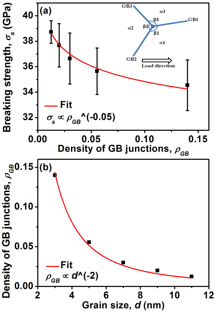
In order to further reveal the physical origin of this correlation between the average grain size and mechanical properties of polycrystalline graphene, we plot the breaking strength vs. GB junction density in Fig. 3(a). It is seen that the breaking strength decreases with increasing density of GB junctions following a power law with an exponent of −0.05. For a brittle material, it is well-known that defect structure and distribution govern its failure properties. As a result, its failure behavior can be described by the weakest-link model, which states that the failure strength of a brittle material follows a power-law relation with the number of weak links in the material28,29. To apply the weakest-link model, it is necessary that the distribution of weak-links is broad and unbounded. In the present context, GB junctions are the weak links. GB junctions are formed by N (N ≥ 3) GBs. The inset in Fig. 3(a) displays a representative GB triple junction. Each grain orientation (α1, α2, and α3) is chosen randomly, thus the grains can take any crystalline orientation. This means that the misorientation between any of the two grains can take any angle from 0 to 60 degrees. It is known that GBs with different misorientations will have different atomic structures, which in turn give rise to different GB energies and different failure strengths. In addition, the angles (β1, β2, and β3) between any of two GBs are also formed randomly. These imply that there are infinitely different configurations of GBs, which give rise to infinitely different configurations of GB junctions. Furthermore, the orientation of the GBs with respect to the loading direction also influences the failure. Since the GBs in our polycrystalline graphene are formed randomly, the formed GBs can take any angle with respect to the loading direction. Also since GB junctions with different angles with respect to the loading direction may have different failure strengths, therefore, they basically are different weak-links, and the number of such configurations is also infinite. Consequently, the distribution of weak-link defects (GB junctions) is broad and unbounded in terms of the number of GB, the grain orientations, the angles between two GBs, and the orientation of the GBs with respect to the loading direction. Hence it is expected that the failure of polycrystalline graphene can be described by the weakest-link model and its failure strength σs should follow a power-law relation with the number of GB junctions or the GB junctions density ρGB, that is, σs ∝ ρGBμ, which is exactly the relation that we have observed in our MD results. The density of GB junctions is scaled with the grain size in an inverse quadratic relation, which is confirmed by our plot shown in Fig. 3(b). As a result, the breaking strength will also follow a power law with the grain size with an exponent of 0.1, and this power law fits nicely with the present MD simulation results as shown in Fig. 2(d), supporting the inverse pseudo Hall-Petch relation. Hence the present work indicates that the breaking strength and the average grain size follow an inverse pseudo Hall-Petch relation.
Figure 3. The correlations among the grain size, the density of GB junctions, and the breaking strength of polycrystalline graphene.
(a) The trend of the breaking strength as a function of the GB junction density (Number of GB junctions per nm2). Inset is the schematic of one GB triple junction configuration. The grain orientations (α1, α2, and α3) are randomly picked. Thus the misorientations between any of two grains are random and can take any value. In addition, the angles (β1, β2, and β3) between two GBs are also formed randomly. Furthermore, the triple junction can form any angle with respect to the loading direction. This also adds in more configurations for GB junctions. Overall, the number of different GB junctions (weak-links) is infinite. (b) The density of GB junctions as a function of the average grain size <d>.
We also consider the effect of the distribution of grain sizes on the mechanical properties of polycrystalline graphene. Figure 4 shows two typical grain size distributions of polycrystalline graphene, with the narrowed grain size distribution being generated from the Voronoi construction30,31,32, and the broad grain size distribution being generated from a continuous nucleation and growth construction forming a Johnson-Mehl microstructure33. For both distributions, we maintain similar number of grains and do not vary the dimensions of the polycrystalline graphene sheet. As a result, the average grain size <d> and the number of GB junctions for both grain size distributions are maintained to be similar (note that the number of grains generated in a continuous nucleation and growth process is random and only an expected number of grains is obtained and not a fixed number). The breaking strength, along with the number of the GB junctions, for the polycrystalline graphene with both grain size distributions are listed in Table 1. It is noted that all the values are also averaged from 5 randomly generated samples with different initial grain configurations but the same average grain size and grain size distribution. Apparently, the width of the grain size distribution does not have any significant effect on the breaking strength. This finding further supports our above statement that the breaking strength of polycrystalline graphene is dictated by the GB junctions.
Figure 4. Two typical distributions of grain size.
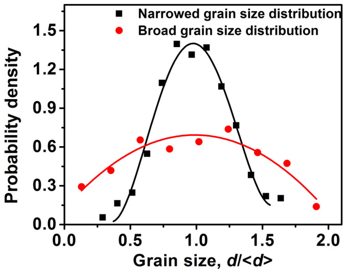
The polycrystalline graphene with the narrowed grain size distribution is generated from the Voronoi construction, while the polycrystalline graphene with the broad grain size distribution is generated from a continuous nucleation and growth construction that forms a Johnson-Mehl microstructure. For these two grain size distributions, the number of grain and the dimensions of the polycrystalline graphene sheet are maintained to be similar. As a result, the average grain size <d> and the number of GB junctions for both grain size distributions are also the same.
Table 1. The breaking strengths, along with the numbers of the GB junctions, for polycrystalline graphene with narrow and broad grain size distributions.
| Breaking strength (GPa) | Number of GB junctions | |
|---|---|---|
| Narrowed grain size distribution | 36.64 ± 2.004 | 80 |
| Broad grain size distribution | 37.47 ± 1.482 | 78 |
It should be noted that the breaking strength measured experimentally also showed a grain size-dependent breaking strength. For example, Lee et al.17 reported that the strength of polycrystalline graphene with an average grain size of ~2.5 μm and 200 μm by means of AFM nanoindentation is 91 and 118 GPa, respectively. It is noted that, in their experiments, atomic force microscopy (AFM) nanoindentation was used to obtain the load-indentation depth curve. Based on this curve, the Young's modulus and breaking strength were then extracted1. Using the present model for polycrystalline graphene, we predict that the breaking strength is 68 and 104 GPa for a grain size of 2.5 μm and 200 μm, respectively – which are in good agreement with the AFM nanoindentation results. Hence, the relation between breaking strength vs. the grain size revealed in the present work provides a plausible explanation for experimentally measured results15,17.
We have shown that the trend of the breaking strength with the grain size in the present work is different from those reported in the previous MD simulations14,16,19. We show below that the reasons for the differences are due to the atomistic models used for polycrystalline graphene. It is noted that some research groups14,19,20,21 manually constructed polycrystalline graphene with regular hexagons for grains and only 5–7 pairs for GBs; while some other groups16,25 constructed polycrystalline graphene with irregular polygons for grains and predominant 5–7 pairs together with a small fraction of squares and octagons for GBs. For example, in Grantab et al.'s simulations14, their model structure is a bicrystalline graphene with specific arrangement of pentagons and heptagons along straight GBs. Besides, no GB junctions were included in their study. But in reality, there must be GB junctions in polycrystalline graphene. This issue was neatly addressed by Song et al.19 In their work, grains took an ideal perfect hexagonal shape and GBs were manually constructed with ideal 5–7 pairs. A pseudo Hall-Petch relation between the failure strength and grain size was observed. In Kotakoski et al.'s work16, the average grain size was varied from 3 to 12 nm, but a fixed number of grains was used for each average grain size. Their simulations showed that the failure strength did not depend on the average grain change in the range of 3–12 nm. Based on the present inverse pseudo Hall-Petch relation, we find that indeed the breaking strength only changes marginally when the average grain size varies from 3 to 12 nm. Hence, the different results on the failure strength obtained by the previous studies arise from the different atomistic models used for polycrystalline graphene. By comparison, the atomic structure for polycrystalline graphene used in the present work contains randomly distributed grain size, shape and crystallographic orientation, thus it is more realistic16 and consistent with pervious experimental observations12,26.
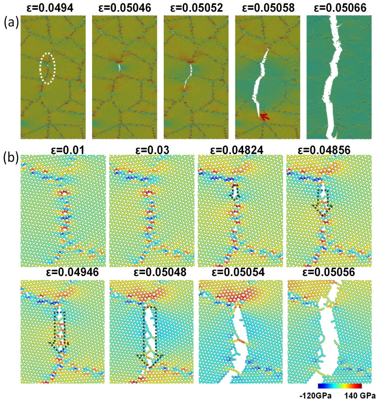
To further understand the failure origin and mechanism, we examine the deformation process of polycrystalline graphene with the different grain sizes under tensile loading. A typical failure process is shown in Fig. 5(a). We first notice that the failure process of polycrystalline graphene is through direct breakage of sp2 C-C bonds, rather than the motion of defects such as dislocations. We further notice that the crack preferentially starts at a GB junction (such as triple, quadruple or higher junctions) wherein one of the connecting GBs is perpendicular or nearly perpendicular to the loading direction. We believe that this is critical to the fracture process in polycrystalline graphene. After crack initiation, the crack propagates along this connecting GB, and then branches out either along connecting GBs or across grain interior along armchair or zigzag paths. The close-up views of crack formation and propagation at a GB junction are shown in Fig. 5(b). Since GB junctions are generally more defected and contain a combination of 5, 7, 8-membered rings, they are less stiff and more compliant, and expected to have a lower load-carrying capacity than grain interior. As a result, the connecting GB which is perpendicular or near perpendicular to the loading direction has to carry extra load. Hence the location that connects this specific GB and the junction is most prone to cracking. It is noted that the intergranular propagation is due to the fact that GBs are generally weaker than the crystalline grain, and the transgranular cracking along armchair or zigzag directions can be explained by the direction-dependent edge energy, as reported in recent MD simulations19 and experiments34.
Figure 5. Deformation process of polycrystalline graphene.
(a) Crack initiation and propagation of both intergranular and transgranular cracks in polycrystalline graphene with average grain size of 11 nm. The white dotted line indicates that the crack preferentially starts at the GB junction point. The red arrow indicates the transgranular crack. (b) The close-up views of crack formation and propagation in GB junction. Atoms are colored according to their atomic stress.
Discussion
We have performed MD simulations to investigate the deformation and failure behavior of polycrystalline graphene under uniaxial tensile loading focusing on the effect of grain size and its distribution on the mechanical properties. The key finding is that the breaking strength is controlled by GB junctions, and the failure preferentially starts from a specific GB junction where one of the connecting GBs is perpendicular or nearly perpendicular to the loading direction. We further show that the breaking strength and grain size follow an inverse pseudo Hall-Petch relation, which is consistent with some experimental measurements. We further show that the weakest-link model provides a physical basis for the observed inverse pseudo Hall-Petch relation.
Methods
The polycrystalline graphene samples are generated using the Voronoi tessellation method30,31,32. Each sample has a length of 50 nm, width of 50 nm, and average grain size ranging from 3 nm to 11 nm. It contains from 26 to 354 randomly oriented grains of various shapes and sizes. The number of grains calculated for a given volume depends on the choice of the average grain size. The grain positions are randomly distributed within the simulation sheet. To avoid grains with artificially high aspect ratios we ensured that the selected positions are not too close to each other. The created polycrystalline graphene sample is annealed to eliminate low or high-density regions near the GBs and junctions. We first anneal the sample at 3000 K for 50 ps after which the sample is quenched to 300 K during a 10 ps run allowing the sample to obtain its equilibrium size (pressure driven to zero)16.
Our MD simulations of polycrystalline graphene are performed using Large-scale Atomic/Molecular Massively Parallel Simulator (LAMMPS)35. The interatomic interaction is described by the adaptive intermolecular reactive empirical bond order (AIREBO) potential36. It should be noted that the smaller cutoff distance in the switching function of AIREBO potential should be taken in the range of 1.92–2.0 Å to avoid a known nonphysical post-hardening behavior37. For the present study, this cutoff distance is set at 2.0 Å25. The uniaxial tensile fracture behavior of the polycrystalline graphene is investigated under a constant strain rate of 4 × 10⁷ s−1 (slower than that typically used in MD simulations16,19,25) in the x direction. The pressure in the y direction is adjusted to 0 GPa to satisfy the zero-stress boundary condition. A constant integration time step of 0.5 fs is used in all the simulations. Periodic boundary conditions are applied in all directions. The stress is calculated from the normal tensor component along the loading direction of the virial stress. The atomic configurations are visualized with the AtomEye package38.
Author Contributions
Z.S.L., T.J.W. and V.B. Shenoy, and Y.W.Z. initiated and guided the project. Z.D.S. performed the MD simulations, analysis of data and prepared figures and the manuscript. S.S.Q. generated the atomic structure of polycrystalline graphene. Q.X.P. advised on the simulation and in the interpretation of the results. All the authors contributed to the research work.
Acknowledgments
Z.D.S., Z.S.L., and T.J.W. are grateful for the support from the National Natural Science Foundation of China through grant numbers 11321062, 11342012, 11372295, and 11372236. Z.D.S. gratefully acknowledges support from the Institute of High Performance Computing (IHPC) under an Agreement for Research Collaboration between IHPC and International Center for Applied Mechanics (ICAM).
References
- Lee C., Wei X., Kysar J. W. & Hone J. Measurement of the elastic properties and intrinsic strength of monolayer graphene. Science 321, 385–388 (2008). [DOI] [PubMed] [Google Scholar]
- Castro Neto A. H., Guinea F., Peres N. M. R., Novoselov K. S. & Geim A. K. The electronic properties of graphene. Rev. Mod. Phys. 81, 109–162 (2009). [Google Scholar]
- Song H. S. et al. Origin of the relatively low transport mobility of graphene grown through chemical vapor deposition. Sci. Rep. 2, 337 (2012). [DOI] [PMC free article] [PubMed] [Google Scholar]
- Chen C. et al. Performance of monolayer graphene nanomechanical resonators with electrical readout. Nat. Nanotechnol. 4, 861–867 (2009). [DOI] [PubMed] [Google Scholar]
- Eda G., Fanchini G. & Chhowalla M. Large-area ultrathin films of reduced graphene oxide as a transparent and flexible electronic material. Nat. Nanotechnol. 3, 270–274 (2008). [DOI] [PubMed] [Google Scholar]
- Geim A. K. & Novoselov K. S. The rise of graphene. Nat. Mater. 6, 183–191 (2007). [DOI] [PubMed] [Google Scholar]
- Li X. et al. Stretchable and highly sensitive graphene-on-polymer strain sensors. Sci. Rep. 2, 870 (2012). [DOI] [PMC free article] [PubMed] [Google Scholar]
- Qiu L., Liu J. Z., Chang S. L. Y., Wu Y. & Li D. Biomimetic superelastic graphene-based cellular monoliths. Nat. Commun. 3, 1241 (2012). [DOI] [PubMed] [Google Scholar]
- Gao L. et al. Repeated growth and bubbling transfer of graphene with millimetre-size single-crystal grains using platinum. Nat. Commun. 3, 699 (2012). [DOI] [PMC free article] [PubMed] [Google Scholar]
- Li X. et al. Large-Area Synthesis of High-Quality and Uniform Graphene Films on Copper Foils. Science 324, 1312–1314 (2009). [DOI] [PubMed] [Google Scholar]
- Li X. et al. Graphene Films with Large Domain Size by a Two-Step Chemical Vapor Deposition Process. Nano Lett. 10, 4328–4334 (2010). [DOI] [PubMed] [Google Scholar]
- Robertson A. W. et al. Spatial control of defect creation in graphene at the nanoscale. Nat. Commun. 3, 1144 (2012). [DOI] [PubMed] [Google Scholar]
- Yu Q. et al. Control and characterization of individual grains and grain boundaries in graphene grown by chemical vapour deposition. Nat. Mater. 10, 443–449 (2011). [DOI] [PubMed] [Google Scholar]
- Grantab R., Shenoy V. B. & Ruoff R. S. Anomalous Strength Characteristics of Tilt Grain Boundaries in Graphene. Science 330, 946–948 (2010). [DOI] [PubMed] [Google Scholar]
- Huang P. Y. et al. Grains and grain boundaries in single-layer graphene atomic patchwork quilts. Nature 469, 389–392 (2011). [DOI] [PubMed] [Google Scholar]
- Kotakoski J. & Meyer J. C. Mechanical properties of polycrystalline graphene based on a realistic atomistic model. Phys. Rev. B 85, 195447 (2012). [Google Scholar]
- Lee G.-H. et al. High-Strength Chemical-Vapor Deposited Graphene and Grain Boundaries. Science 340, 1073–1076 (2013). [DOI] [PubMed] [Google Scholar]
- Ruiz-Vargas C. S. et al. Softened Elastic Response and Unzipping in Chemical Vapor Deposition Graphene Membranes. Nano Lett. 11, 2259–2263 (2011). [DOI] [PubMed] [Google Scholar]
- Song Z., Artyukhov V. I., Yakobson B. I. & Xu Z. Pseudo Hall-Petch Strength Reduction in Polycrystalline Graphene. Nano Lett. 13, 1829–1833 (2013). [DOI] [PubMed] [Google Scholar]
- Wei Y. et al. The nature of strength enhancement and weakening by pentagon-heptagon defects in graphene. Nat. Mater. 11, 759–763 (2012). [DOI] [PubMed] [Google Scholar]
- Zhang J., Zhao J. & Lu J. Intrinsic Strength and Failure Behaviors of Graphene Grain Boundaries. Acs Nano 6, 2704–2711 (2012). [DOI] [PubMed] [Google Scholar]
- Rasool H. I., Ophus C., Klug W. S., Zettl A. & Gimzewski J. K. Measurement of the intrinsic strength of crystalline and polycrystalline graphene. Nat. Commun. 4, 2811 (2013). [Google Scholar]
- Liu Y. & Yakobson B. I. Cones, Pringles, and Grain Boundary Landscapes in Graphene Topology. Nano Lett. 10, 2178–2183 (2010). [DOI] [PubMed] [Google Scholar]
- Yazyev O. V. & Louie S. G. Topological defects in graphene: Dislocations and grain boundaries. Phys. Rev. B 81, 195420 (2010). [Google Scholar]
- Zhang T., Li X., Kadkhodaei S. & Gao H. Flaw Insensitive Fracture in Nanocrystalline Graphene. Nano Lett. 12, 4605–4610 (2012). [DOI] [PubMed] [Google Scholar]
- Biro L. P. & Lambin P. Grain boundaries in graphene grown by chemical vapor deposition. New J. Phys. 15, 035024 (2013). [Google Scholar]
- Malola S., Hakkinen H. & Koskinen P. Structural, chemical, and dynamical trends in graphene grain boundaries. Phys. Rev. B 81, 165447 (2010). [Google Scholar]
- Alava M. J., Nukala P. K. V. V. & Zapperi S. Size effects in statistical fracture. J. Phys. D: Appl. Phys. 42, 214012 (2009). [Google Scholar]
- Weibull W. A statistical distribution function of wide applicability. J. Appl. Mech. 18, 293–297 (1951). [Google Scholar]
- Brostow W., Dussault J. P. & Fox B. L. Construction of voronoi polyhedra. J. Comput. Phys. 29, 81–92 (1978). [Google Scholar]
- Finney J. L. Procedure for the construction of voronoi polyhedra. J. Comput. Phys. 32, 137–143 (1979). [Google Scholar]
- Tanemura M., Ogawa T. & Ogita N. A new algorithm for 3-dimensional voronoi tessellation. J. Comput. Phys. 51, 191–207 (1983). [Google Scholar]
- Frost H. J. & Thompson C. V. The effect of nucleation conditions on the topology and geometry of two-dimensional grain structures. Acta metall. 35, 529–540 (1987). [Google Scholar]
- Kim K. et al. Ripping Graphene: Preferred Directions. Nano Lett. 12, 293–297 (2012). [DOI] [PubMed] [Google Scholar]
- Plimpton S. Fast parallel algorithms for short-range molecular-dynamics. J. Comput. Phys. 117, 1–19 (1995). [Google Scholar]
- Stuart S. J., Tutein A. B. & Harrison J. A. A reactive potential for hydrocarbons with intermolecular interactions. J. Chem. Phys. 112, 6472–6486 (2000). [Google Scholar]
- Pastewka L., Pou P., Perez R., Gumbsch P. & Moseler M. Describing bond-breaking processes by reactive potentials: Importance of an environment-dependent interaction range. Phys. Rev. B 78, 161402 (2008). [Google Scholar]
- Li J. AtomEye: an efficient atomistic configuration viewer. Modelling Simul. Mater. Sci. Eng. 11, 173–177 (2003). [Google Scholar]


