Abstract
Klockmannite copper selenide nanosheets (CuSe NSs) are synthesized by a facile microwave-assisted method and fully characterized. The nanosheets have smooth surface and hexagonal shape. The lateral size is 200–500 nm × 400–800 nm and the thickness is 55 ± 20 nm. The current-voltage characteristics of CuSe NS films show unique Ohmic and high-conducting behaviors, comparable to the thermally-deposited gold electrode. The high electrical conductivity of CuSe NSs implies their promising applications in printed electronics and nanodevices. Moreover, the local electrical variation is observed, for the first time, within an individual CuSe NS at low bias voltages (0.1 ~ 3 V) by conductive atomic force microscopy (C-AFM). This is ascribed to the quantum size effect of NS and the presence of Schottky barrier. In addition, the influence of the molar ratio of Cu2+/SeO2, reaction temperature, and reaction time on the growth of CuSe NSs is explored. The template effect of oleylamine and the intrinsic crystal nature of CuSe NS are proposed to account for the growth of hexagonal CuSe NSs.
Transition metal chalcogenides are fundamentally and technologically important for numerous applications such as photo-catalysis, photo-electric devices, and energy-harvesting and storage devices1,2. Copper selenides represent one kind of the most important metal chalcogenides. They are composed of a variety of stoichiometric and nonstoichiometric phases including cubic berzelianite (Cu2Se, Cu1.8Se and Cu2-xSe), tetragonal umangite (Cu3Se2), hexagonal klockmannite (CuSe and Cu0.87Se), and orthorhombic athabascaite (Cu5Se4, CuSe)3. All these phases are identified as p-type semiconductors due to the existence of copper vacancies within crystal lattice, and widely used in solar cells4,5, gas sensors6, and photo-detectors7. Instead of crystal phases, efforts have also been devoted to preparing copper selenides with controlled morphologies such as nanoparticles8,9,10,11, nanocubes12,13, nanotubes14, nanowires15,16 and hierarchical nanostructures17,18.
Besides zero- (0D) and one-dimensional (1D) ones, two-dimensional (2D) copper selenides (nanosheets and nanoplates) have recently attracted increasing interest as inspired by graphene19,20. Choi et al. synthesized cubic-phase Cu2-xSe nanodiscs by using imidazoline-2-selenone as selenium precursor and investigated their photo-response behavior21. Deng et al. prepared single-crystal nanosheets and nanoplates of berzelianite Cu2-xSe22. These progresses enable us to explore novel properties and potential applications of 2D copper selenides. However, the synthesis of 2D copper selenides is generally time-consuming or needs additional capping agents. Moreover, in comparison with nonstoichiometric Cu2Se and Cu2-xSe, relatively limited studies have been carried out for 2D stoichiometric CuSe23,24,25.
On the other hand, probing the electrical transport properties of individual 2D nanostructure can provide deep insight into the correlation between crystal structure and performance of electronic devices. Recently, Xue et al. reported an anisotropic photoresponse of single germanium selenide (GeSe) nanosheet. The on/off switching ratio of device perpendicular to the nanosheet is 3.5 times higher than that parallel to the nanosheet26. However, to the best of our knowledge, systematic investigation on the electrical properties of individual nanostructures of 2D CuSe is still lacking as well as their films. This is possibly due to the lack of facile and effective method for the synthesis of high-quality 2D CuSe nanostructures.
Herein, we report the controlled synthesis of single-crystalline CuSe nanosheets (NSs) by a facile microwave-assisted approach. The influence of the molar ratio of Cu2+/SeO2, reaction temperature and reaction time on the growth of CuSe NSs is investigated, and a possible growth mechanism is proposed. Moreover, the electrical transport properties of the as-prepared CuSe NS film and individual CuSe NS are explored.
Results
Characterization of CuSe NSs
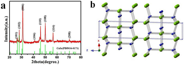
The phase and purity of CuSe NSs are characterized by X-ray diffraction (XRD). All the diffraction peaks in the XRD pattern (Fig. 1a) can be accurately indexed to the hexagonal klockmannite phase of CuSe (JCPDS No. 34-0171, a = b = 3.939 Å, c = 17.25 Å, Pmmc 63). No diffraction peaks of other impurities are found in the XRD pattern, indicating that the product is pure CuSe. Moreover, the intensity of (006) peak is much stronger than that of other peaks, implying that the as-prepared CuSe NSs are oriented along <001> direction. This is in good agreement with the highly anisotropic crystal structure and the weak interaction between the (001) planes in the klockmannite phase (Fig. 1b).
Figure 1.
(a) XRD pattern of as-prepared CuSe nanosheets. (b) Crystal structure of klockmannite CuSe. The light green shaded atoms represent Se, while the deep blue shaded atoms represent Cu.
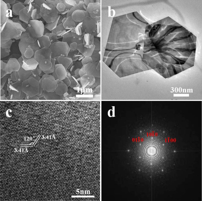
The morphology and size of CuSe NSs are investigated by field-emission scanning electron microscopy (FE-SEM) and transmission electron microscopy (TEM). Fig. 2a shows a typical FE-SEM image of CuSe NSs, revealing hexagonal and quasi-hexagonal shapes, which have smooth surfaces (Fig. 2b). The average lateral size of CuSe NSs extracted from SEM image is 200–500 nm × 400–800 nm, while the thickness analyzed by atomic force microscopy (AFM, Fig. S1) is 55 ± 20 nm. Fig. 2c shows a typical high-resolution (HR) TEM image of single CuSe NS, revealing the well-resolved 2D lattice fringes. The values of 3.41 and 3.41 Å match well with the inter-planar d-spacing of the (100) and (010) planes of klockmannite CuSe, respectively. The intersection angle of ~120° is identical to the theoretical value between the (100) and (010) planes of klockmannite CuSe. The fast Fourier transform pattern (Fig. 2d) taken from the HR-TEM image (Fig. 2c) also implies the single-crystalline hexagonal structure with the surface is normally oriented along the [001] direction. The above results are consistent with the preferable [006] orientation observed by XRD (Fig. 1a). In addition, the energy-dispersive X-ray spectrum (EDS, Fig. S2) only reveals two strong peaks of Cu and Se elements besides the peak of Si substrate. The quantitative EDS analysis shows that the atom ratio of Cu and Se is close to the intrinsic 1:1 stoichiometry, implying the homogeneous purity of CuSe NSs.
Figure 2.
(a) FE-SEM and (b) TEM images of as-prepared CuSe nanosheets. (c) HR-TEM lattice image of a single CuSe nanosheet. (d) The fast Fourier transform pattern taken from HR-TEM image (Fig. 2c).
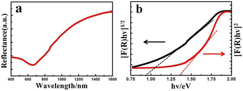
The optical band gap of CuSe NSs, a crucial electronic parameter for semiconductor nanomaterials, is explored by diffuse reflectance spectroscopy. Typical spectrum (Fig. 3a) shows that the onset of absorption for CuSe NSs is near 1400 nm. By applying Kubelka-Munk transformation27,28, a plot of [F(R)hν]1/2 versus energy yields an indirect band gap of 0.94 eV, while a plot of [F(R)hν]2 versus energy yields a direct band gap of 1.36 eV (Fig. 3b). By using the direct band-gap method, the band edge is blue-shifted by ~0.31 eV in relation to bulk CuSe (1.05 eV)8,29. The band structure of CuSe NSs is also studied by cyclic voltammetry (CV, Fig. S3)30. The onset potential of the reduction of pyridine-treated CuSe NSs appears at −0.2 V vs. Ag/Ag+. Therefore, the bottom of the conduction band (the lowest unoccupied molecular orbital, LUMO) can be determined as −4.51 eV from vacuum level. Moreover, in view of the direct optical band gap of CuSe NSs (1.36 eV), the top of the valence band (the highest occupied molecular orbital, HOMO) can be determined as −5.87 eV.
Figure 3.
(a) Typical diffuse reflectance spectra for CuSe nanosheets. (b) Plots of [F(R)hν]1/2 and [F(R)hν]2 vs energy for the CuSe nanosheets, from which indirect and direct band-gap energies are obtained.
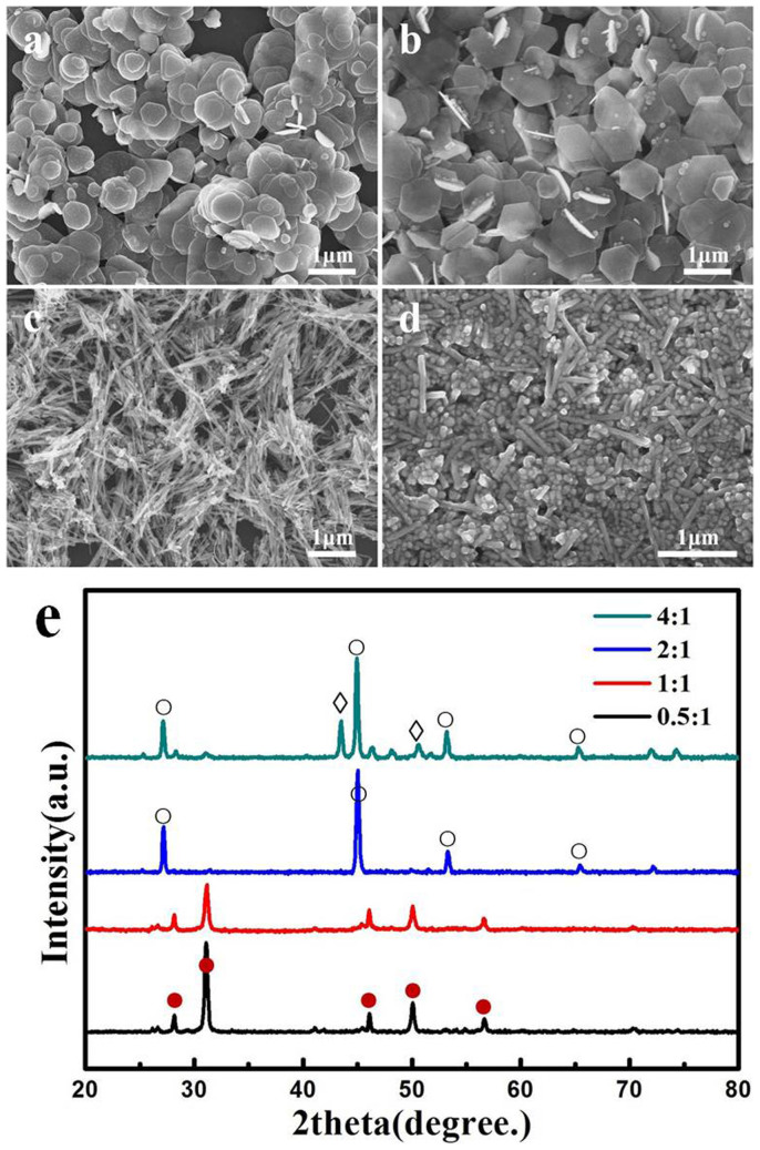
Fig. 4 shows a set of typical SEM images and XRD patterns of the products obtained at different molar ratios of Cu2+ to SeO2, while the other parameters are fixed. Quasi-circular and truncated-triangular nanoplates are formed at a molar ratio of 0.5:1 (Fig. 4a), while hexagonal NSs are obtained at a molar ratio of 1:1 (Fig. 4b). The XRD patterns (Fig. 4e) confirm that both nanoplates and nanosheets have the same klockmannite phase. Note that instead of discrete ones, the nanoplates are prone to stack with each other. Similar phenomenon is observed for berzelianite nanoplates in the literature22. When the molar ratio is increased to 2:1 (Fig. 4c), berzelianite Cu2Se nanowires with the diameter of 30 ± 10 nm and the length of several micrometers become dominant (Fig. S4a). The typical lattice spacing is ~3.32 Å (Fig. S4b), which is consistent with the (111) plane spacing of cubic berzelianite Cu2Se phase (JCPDS No. 88-2044, a = 5.787 Å, Fm-3m). Further increasing the molar ratio to 4:1, a mixture of nanoparticles and nanorods is obtained (Fig. 4d). The XRD pattern reveals a blend of berzelianite Cu2Se and Cu. The berzelianite Cu2Se phase is confirmed by HR-TEM (Fig. S4d) and a lattice spacing of 3.3 Å is revealed. Nevertheless, the formation of Cu phase is due to the reduction of excessive Cu2+ by oleylamine (OM) and the lack of SeO2 source. The above results indicate that the molar ratio of Cu2+ to SeO2 play an important role in the morphology and crystal phase of the final products. This is likely due to different redox reaction rates under different kinetic conditions. Highly anisotropic structures tend to become favorable in a slow reduction process31,32. Specifically, with a molar ratio of 2:1, Cu2+ ions are reduced by OM into Cu+ ions, which can react with SeO2. The resultant cubic Cu2Se tends to grow into nanowires due to the anisotropic growth. When the molar ratio is 4:1, the reaction rate increases remarkably and more Cu2Se seeds emerge, favoring the isotropic growth in the early stage. As the reaction proceeds, a number of Cu2+ ions are consumed, thereby resulting in lower reduction rates. Meanwhile, the isotropic growth is switched to the anisotropic one, leading to the formation of Cu2Se nanorods.
Figure 4.
(a–d) FE-SEM images and (e) XRD patterns of the products prepared with the different molar ratios of Cu2+ to SeO2: (a) 0.5:1, (b) 1:1, (c) 2:1 and (d) 4:1. The diffraction peaks are marked by: (•) klockmannite hexagonal CuSe, JCPDS No. 34-0171; (○) berzelianite cubic Cu2Se, JCPDS No. 88-2044 and (◊) cubic Cu, JCPDS No. 03-1018.
Besides the molar ratio of Cu2+ to SeO2, the influence of reaction temperature and time on the growth of CuSe NSs is also investigated. Fig. S5 shows SEM images and XRD patterns of the products obtained at different reaction temperatures, while the other parameters are fixed. With the increase of reaction temperature, the amount and size of NSs increase accordingly, while the amount of particles decreases. Moreover, instead of pure klockmannite phase at 180°C, a blend of klockmannite CuSe and berzelianite Cu2Se are obtained at 140 and 160°C. The coexistence of two phases becomes more obvious at 200°C. This is likely due to the appropriate competition and balance between two phases under thermodynamic conditions. As described previously33,34, the berzelianite Cu2Se is thermodynamically more stable than the klockmannite CuSe, and a phase transformation can arise between the two phases.
Discussion
To reveal the growth mechanism of klockmannite CuSe NSs, the products at different reaction time are collected and investigated with SEM (Fig. S6). Hexagonal NSs with the lateral size of 100–300 nm × 300–500 nm are obtained together with a few nanoparticles in 1 min. As the reaction goes on from 5, 20, to 60 min, the amount and size of NSs are increased while the content of particles in the products is decreased. Further increasing the reaction time to 120 min, the amount and size of CuSe NSs keep almost unchanged, suggesting a drastic ‘size-defocusing’ process35. On the basis of above results, it can be assumed that the formation of CuSe NSs is controlled by kinetic dynamics, i.e., going through the initial crystalline nucleation followed by the oriented growth of CuSe crystal seeds.
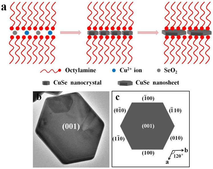
Specifically, OM can act as not only an effective stabilizing ligand to protect the crystal from aggregating, but also a strong binding agent to template-guide the preferential growth of CuSe NSs (Fig. 5a). The introduction of octylamine enhances the templating effect and improves the yield of CuSe NSs (Fig. S7). Such a template-guided effect is also observed in the direct growth of ultrathin CuS nanosheets36, ultrathin ZnSe nanosheets37 and CdSe nanosheets38. On the other hand, the final shape of nanocrystals is determined by the ratio of the growth rates of different crystallographic planes. As for the hexagonal nanocrystals (Fig. 5b and 5c), it is mainly determined by the growth rates (R) along the [110], [010] and [100] directions. The classic BFDH model assumes the growth velocity (Rhkl) of a face on a growing polygon is approximately inversely proportional to the inter-planar spacing (dhkl)39. For CuSe NSs, d001 (17.25 Å) > d100 (3.41 Å) = d010 (3.41 Å) > d110 (1.97 Å), i.e., the growth rate sequence of R110 > R100 = R010 > R001. In addition, the crystal growth along the z axis proceeds slowly due to the weak van der Waals character between the layers. This leads to the formation of anisotropic 2D nanostructures oriented along the [001] direction. Thus, besides the templating effect of OM (and octylamine), the intrinsic crystal nature of klockmannite CuSe and different growth rates of exposed crystal planes are accounted for the evolution from small particles to hexagonal NSs.
Figure 5.
(a) Schematic illustration of the growth of CuSe nanosheets. (b) TEM image of single CuSe nanosheet. (c) Schematic diagram of the hexagonal crystal with the indexed facets.
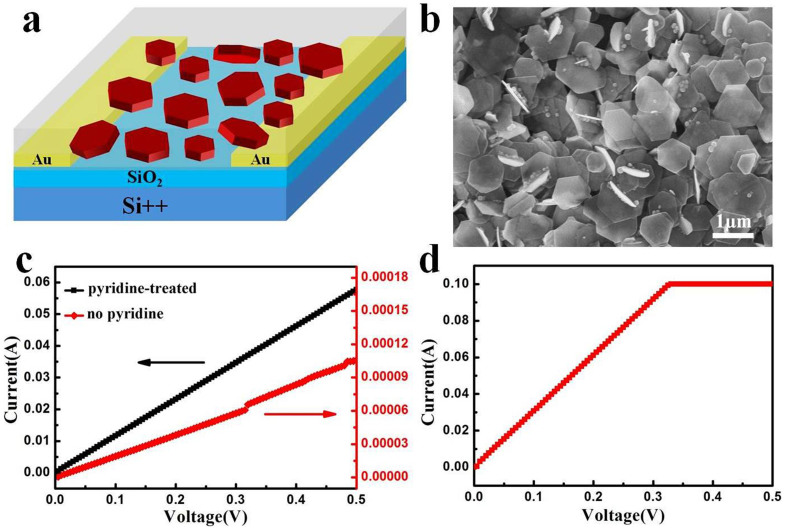
To explore the electrical properties of CuSe NSs, a prototype device is fabricated (Fig. 6a). The device is fabricated by dropping 20 μL CuSe NS solution onto pre-patterned Au electrodes. The solvent is dried by vacuum-annealing at 40°C for 30 min. It can be seen that CuSe NSs are interconnected and stack into a compact film (Fig. 6b). Fig. 6c shows the typical current-voltage (I-V) characteristics of the device. The observation of almost linear response demonstrates an Ohmic rather than semiconducting behavior of CuSe NSs. Note that the device with pyridine treatment shows more excellent electrical conductivity than that without pyridine treatment. At a bias voltage of 500 mV, currents of about 10−5 and 10−2 A are recorded for the devices before and after pyridine treatment, respectively. This is a substantial increase in current by about three orders of magnitude. As discussed previously40,41, the original OM adsorbed on CuSe NSs could be removed with pyridine treatment and consequently the charge mobility in NS thin film is improved significantly. The effect of pyridine is similar to short hydrocarbon ligands such as mercaptopropionic acid, ethylenediamine, and ethanedithiol, which are used to reduce inter-particle distance and enhance inter-particle coupling9. The high-conducting behavior is further explored by measuring the Hall Effect in the pyridine-treated CuSe NS film with the thickness of ~20 μm. The results show that the CuSe NS film resides in the P-type conduction. The hole mobility and the carrier density give the values of 1.87 cm2 V−1 s−1 and 3.01 × 10²¹/cm3, respectively, which is comparable with vapor-deposited Cu2-xSe thin films42. Moreover, the conductivity of pyridine-treated CuSe NS film is almost identical to that of thermally-deposited Au electrode (Fig. 6d). The above results enlighten us to develop a novel and promising low-cost semiconductor material in place of traditional noble metals (Au, Ag, Cu et al) for high-performance electronic conductors. In addition, in view of the band gap of CuSe NSs (Fig. 3b), the photoconductivity of CuSe NS thin film is also investigated. It is unexpected that the current shows no obvious changes before and after illumination (Fig. S8). This could be due to the intrinsic high carrier concentration of CuSe NSs, which may depress the changes in photo-excited carriers upon illumination9.
Figure 6.
(a) Schematic illustration and (b) representative SEM image of a device based on CuSe NSs film. (c) I–V characteristics of CuSe NSs film before and after pyridine treatment. (d) I–V characteristics of thermally-deposited Au electrode.
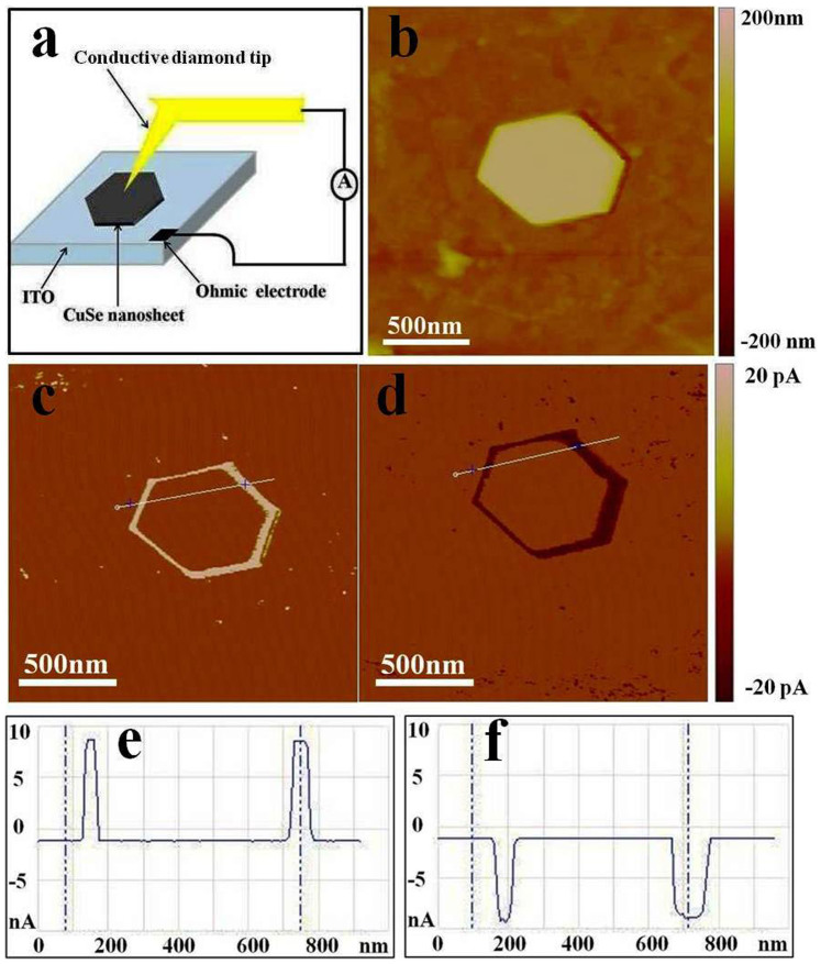
To reveal the intrinsic electrical properties, the I-V characteristics of single CuSe NS is explored and the current distribution is mapped by conductive AFM (C-AFM), which is an effective technique to probe local conduction with nanoscale spatial resolution. Fig. 7a shows a schematic diagram of single CuSe NS-based AFM electrical circuit, in which ITO is used as the bottom electrode. The electrical characterization is applied in contact mode with a conductive diamond tip. The bias voltage is applied to the sample while keeping the tip grounded. Fig. 7b–f show topography and typical C-AFM images of single CuSe NS by point-to-point tip scanning. The targeted CuSe NS has uniform thickness and smooth surface (Fig. S9). By applying a dc bias voltage of 100 mV, the currents in fringe region can reach ~10 nA, while no obvious currents occurs in the middle region (Fig. 7c, e). The same local conduction currents are also observed when the bias voltage is reversed (Fig. 7d, f). The above observation indicates a substantial conductivity difference between the middle and fringe regions of hexagonal CuSe NS.
Figure 7.
(a) Schematic diagram of single CuSe nanosheet-based electrical circuit for C-AFM measurement. (b) Topography and (c, d) current images of CuSe nanosheet are obtained simultaneously under the C-AFM mode. The applied bias voltage is (c) 100 mV and (d) −100 mV. (e, f) Spatial profiles of the current along corresponding lines in the C-AFM images (c, d).
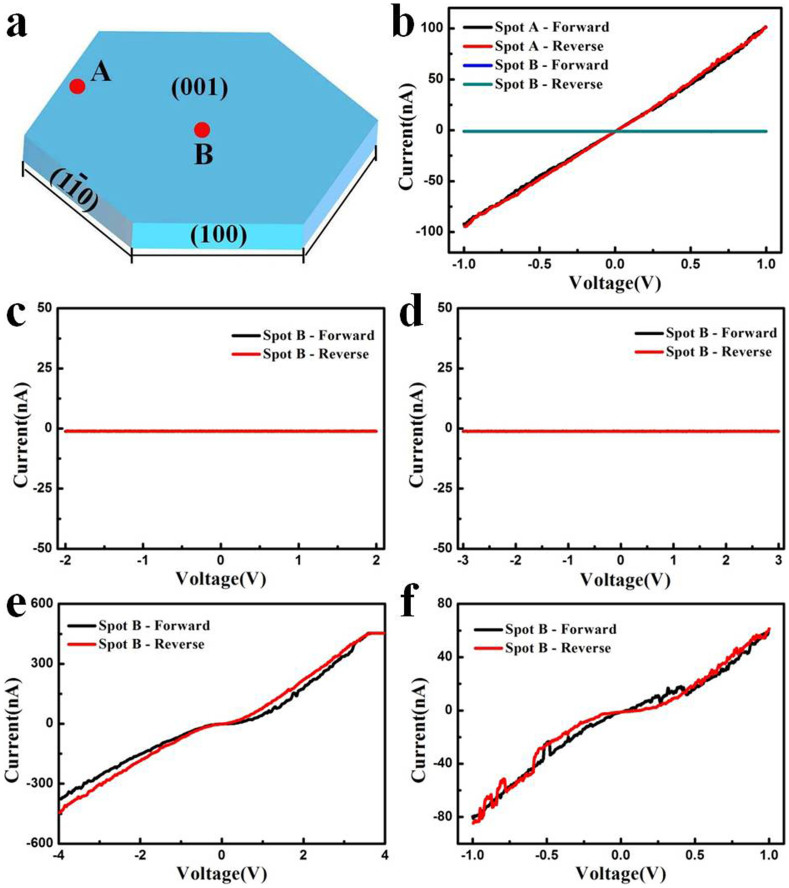
To reveal the local electrical variation more quantitatively, the I–V characteristics of two representative spots A and B on the surface of single CuSe NS are investigated (Fig. 8a). As a bias voltage varies from −1 V to 1 V and reversely, a linear and symmetric curve is observed for spot A, indicating a typical Ohmic behavior. An electric resistance on the order of 107 ohms chimed in with the inferior conductivity of NS film without pyridine-treatment. In contrast, no obvious I–V characteristics are observed for spot B (Fig. 8b). The different I-V characteristics for spots A and B confirms the local electrical variation of CuSe NS. However, as the bias voltage is up to 4 V, a nonlinear and almost symmetric I-V characteristics is obtained (Fig. 8c–e), similar to those of individual silver trimolybdate nanowire43, Sb2S3 nanowire44, and NH4V3O8 nanobelt45. The I–V characteristics for spot B kept similar semiconducting behavior while the bias voltage decreases back to 100 mV (Fig. 8f), where the electric resistance is close to that of spot A.
Figure 8.
(a) Schematic diagram of marked spots located in the surface of hexagonal crystal with the indexed facets. A represents fringe region, and B represents middle region. (b) I-V curves of two marked spots by C-AFM. The applied bias was swept from −1 to 1 V and reversely. (c–e) I-V curves of spot B by C-AFM. The applied bias voltages were 2 V (c), 3 V (d) and 4 V (e). (f) I-V curve of spot B by C-AFM. The applied bias voltages were reduced reversely to 1 V.
The variation in the electrical properties for spot B is partly due to residual ethanol and trace OM adsorbed on CuSe NSs (FT-IR, Fig. S10), which can passivate the surfaces of nanosheets and inhibit the active transport of carriers. Moreover, the CuSe-diamond tip and CuSe-ITO contacts can be considered as Schottky diode due to typical potential barrier between semiconductor and metal (Fig. S11), and thereby the current device is regarded as two back-to-back Schottky diodes44. The carriers can't transport effectively through the CuSe NS until the applied voltage is high enough to overcome the Schottky barrier height at the CuSe-ITO (or diamond tip) interface. Another possible reason may be related to the intrinsic crystal structure of klockmannite CuSe, which consists of alternating CuSe3-Cu3Se-CuSe3 layers and Se–Se layers along the z axis. The interaction of CuSe3-Cu3Se-CuSe3 layers is covalent bonds, while the interaction of Se–Se layers is van der Waals force. Due to weak interaction and large inter-layer spacing (2.38 Å), the gap between the Se–Se layers along [001] direction may form a ‘blocking barrier’. As a result, the effective transport (or hopping) of intrinsic carriers will be delayed unless the threshold voltage is attained. In contrast with spot B, higher conductivity of fringe area (spot A) is likely due to the quantum size effect of CuSe NS. This is similar to the MoS2 NSs46,47, in which some low-coordination step-edges and corner atoms induce additional local chemical effect that dominates over the basal plane atoms. As a consequence, the electronic structure of fringe area is changed significantly and becomes more metallic. Namely, there is a preferable conducting pathway for spot A. Nonetheless, the intrinsic mechanism is still uncertain, but we speculate that a deeper understanding for surface structure and surface energy of individual CuSe NS will be helpful to account for the local variety of C-AFM.
In summary, a facile microwave-assisted method has been developed to synthesize the klockmannite CuSe NSs, which have hexagonal shape and smooth surface. The lateral size of as-prepared CuSe NSs is 200–500 nm × 400–800 nm and the thickness is 55 ± 20 nm. The molar ratio of Cu2+/SeO2, reaction temperature, and reaction time are found to play an important role in the growth of CuSe NSs. The template effect of OM and the intrinsic crystal nature of CuSe NS are proposed to account for the growth of hexagonal CuSe NSs. More importantly, the pyridine-treated CuSe NS film shows unique Ohmic and high-conducting behavior, comparable to that of thermally-deposited gold electrode. The local electrical variation of an individual CuSe NS is observed at the low bias voltages (0.1 ~ 3 V) by C-AFM, which is mainly ascribed to the quantum size effect of NS and the presence of Schottky barrier. The facile synthesis and exceptional electrical properties of the CuSe NSs would pave a promising way for their practical application in flexible electronics and nanodevices.
Methods
Chemicals
Copper (II) acetate, monohydrate [Cu(CH3COO)2·H2O, analytical reagent], selenium dioxide (SeO2, spectroscopic reagent), and tetrabutylammonium perchlorate (TBAP, 98%) were purchased from Sinopharm Chemical Reagent Co., Ltd. n-Octylamine (99%) and oleylamine (OM, 80 ~ 90%) were purchased from Aladdin Chemistry Co., Ltd. Organic solvents e.g., chloroform, ethanol, and pyridine, were of analytical grade and obtained from Sinopharm Chemical Reagent Co., Ltd. All chemicals were used as received.
Synthesis of CuSe NSs
All the synthesis was performed in a microwave system (2.45 GHz, 300 W, Discover S-Class, CEM). In a typical process, 10 mg Cu(CH3COO)2·H2O, 5.5 mg SeO2, and 5 mL OM were mixed in a 10 mL microwave vial and capped. The mixed solution was magnetically stirred at room temperature overnight, and the vial was transferred into the microwave system and heated at 180°C for 1 h. When the reaction was completed, the suspension changed color from blue-green to black, implying the formation of CuSe NSs. The resulting black products were centrifuged and washed with excess ethanol. The as-prepared CuSe NSs were further dispersed in chloroform (or n-hexane) for characterization. To further control the size and morphology of CuSe NSs, the effect of the reaction parameters such as the molar ratio of Cu(CH3COO)2·H2O and SeO2, reaction temperature, and reaction time was explored. Note that only one parameter is varied, while the other ones are fixed.
Cyclic voltammetry
Cyclic voltammetry was undertaken at room temperature with a CHI660D potentiostat/galvanostat and used a three-electrode cell arrangement. Glassy carbon was used as the working electrode, Pt wire was as the counter electrode, and Ag/Ag+ (0.01 M AgNO3 in acetonitrile) was as the reference electrode. The electrolyte was prepared by dissolving tetrabutylammonium hexafluorophosphate (TBAPF6) in acetonitrile (0.1 M). To obtain well-defined reduction signals, the CuSe NSs were treated by pyridine and washed at least three times to remove the excess OM. A concentrated suspension of CuSe NSs in chloroform was drop-casted onto glassy carbon and dried under vacuum for 10 min. Before measurements, the solvent and electrolyte were thoroughly deoxygenated by bubbling with high-purity nitrogen for 20 min and a nitrogen atmosphere was kept in the whole process. The scan rate was fixed at 30 mV/s. The LUMO energy levels were calculated from the onset reduction potential (E'red), according to: ELUMO = −Ea = −(E'red + 4.71) eV, where potential values are relative to the Ag/Ag+ reference electrode. As shown in Fig. S3, the onset potential of reduction near −0.2 V was obtained from the Ag/Ag+ reference electrode, corresponding to a LUMO of −4.51 eV from vacuum level.
Conductivity properties of CuSe NSs film
Conductivity properties of devices were recorded with Keithley 4200 SCS and SUSS PM8 probe station in a clean and shielded box at room temperature. Firstly, the interdigitated Au electrodes with 4 fingers (width 20 μm, length 200 μm, interfinger spacing 20 μm) were fabricated by photolithography and electron beam deposition of Au on Si substrate covered with 300 nm thick SiO2. The pre-patterned electrodes were cleaned with acetone, ethanol and de-ionized water. For pyridine treatment, the CuSe NSs were purified thoroughly by pyridine, washed at least three times, and dispersed in the chloroform. The devices were fabricated by dropping 20 μL of CuSe solution onto pre-cleaned Au electrodes and dried by vacuum-annealing at 40°C for 30 min. Similar procedure was also used for investigating the photoconductivity properties of CuSe NSs film. A xenon lamp was used as the white light source for the photocurrent measurements.
Electrical properties of single CuSe NS
Electrical properties of single CuSe NS were explored by atomic force microscope (AFM, Dimension3100, Veeco) at ambient conditions. The electrical current was applied locally scanning in contact mode. The scan rate was set at 1 Hz. Silicon cantilever coated by conductive diamond (DCP11 by NT-MDT) was used as tip, and ITO glass was used as substrate. A drop of chloroform solution with the dispersed CuSe NSs was dropped onto the pre-cleaned ITO glass and dried naturally. The bias voltages were applied to the ITO substrate through conventional metal Ohmic electrodes, while the conductive tip was grounded. A preamplifier box was used to acquire high signal-to-noise sample current.
Characterization
The products were characterized by X-ray diffraction (XRD) on Bruker D8 Advance powder X-ray diffractometer at a scanning rate of 0.04° s−1 in the 2θ range of 20 to 80°, using Cu-Kα radiation (λ = 1.5406 Å). The morphology and structure were examined on Hitachi-S4800 scanning electron microscope (SEM) at 10 KV and Tecnai G2 F20 S-Twin transmission electron microscope (TEM) at an acceleration of 200 KV. High resolution TEM images and selected area electron diffraction (SAED) patterns were taken simultaneously on Tecnai G2 F20 S-TEM. For SEM and TEM measurement, a drop of chloroform solution with the dispersed CuSe NSs was casted onto a piece of silicon and a carbon-coated Cu grid, respectively. The solvent was allowed to evaporate in air at room temperature. Energy-dispersive X-ray spectrometry (EDS) analysis was performed on the Quanta 400 FEG SEM at 20 KV. Diffuse reflectance UV-vis absorption spectra (DRS) were performed on Perkin-Elmer Lambda 750 equipped with a 60 mm integrating sphere in the range of 400–1400 nm. Fourier transform infrared (FTIR) spectra were acquired with Nicolet 760 FTIR spectrometer in a KBr pellet, scanning from 4000 to 400 cm−1 at room temperature.
Author Contributions
Y.L. and G.P. designed the research and co-wrote the paper. Y.L., F.W., Y.X. and H.P. performed the synthesis experiment and sample characterization. H.Z., Z.L. and Y.L. conducted the C-AFM study and analyzed the data.
Supplementary Material
Supplementary Information
Acknowledgments
This work was supported by the National Natural Science Foundation of China (No. 21273272), the National Basic Research Program of China (No. 2010CB934100), and the Chinese Academy of Sciences.
References
- Wang Q. H., Zadeh K. K., Kis A., Coleman J. N. & Strano M. S. Electronics and optoelectronics of two-dimensional transition metal dichalcogenides. Nat. Nanotech. 7, 699–712 (2012). [DOI] [PubMed] [Google Scholar]
- Gao M. R., Xu Y. F., Jiang J. & Yu S. H. Nanostructured metal chalcogenides: synthesis, modification, and applications in energy conversion and storage devices. Chem. Soc. Rev. 42, 2986–3017 (2013). [DOI] [PubMed] [Google Scholar]
- Xie Y., Zheng X. W., Jiang X. C., Lu J. & Zhu L. Y. Sonochemical synthesis and mechanistic study of copper selenides Cu2-xSe, β-CuSe, and Cu3Se2. Inorg. Chem. 41, 387–392 (2002). [DOI] [PubMed] [Google Scholar]
- Hamilton C. E., Flood D. J. & Barron A. R. Thin film CdSe/CuSe photovoltaic on a flexible single walled carbon nanotube substrate. Phys. Chem. Chem. Phys. 15, 3930–3938 (2013). [DOI] [PubMed] [Google Scholar]
- Chen W. S., Stewart J. M. & Mickelsen R. A. Polycrystalline thin film Cu2-xSe/CdS solar cell. Appl. Phys. Lett. 46, 1095–1097 (1985). [Google Scholar]
- Wang Z. H. et al. Template synthesis of Cu2-xSe nanoboxes and their gas sensing properties. CrystEngComm 14, 3528–3533 (2012). [Google Scholar]
- Kou H. H., Jiang Y. M., Li J. J., Yu S. J. & Wang C. M. Enhanced photoelectric performance of Cu2-xSe nanostructure by doping with In3+. J. Mater. Chem. 22, 1950–1956 (2012). [Google Scholar]
- Malik M. A., O'Brien P. & Revaprasadu N. A novel route for the preparation of CuSe and CuInSe2 nanoparticles. Adv. Mater. 17, 1441–1444 (1999). [Google Scholar]
- Liu X. et al. Size-controlled synthesis of Cu2-xE (E = S, Se) nanocrystals with strong tunable near-infrared localized surface plasmon resonance and high conductivity in thin films. Adv. Funct. Mater. 23, 1256–1264 (2013). [Google Scholar]
- Riha S. C., Johnson D. C. & Prieto A. L. Cu2Se nanoparticles with tunable electronic properties due to a controlled solid-state phase transition driven by copper oxidation and cationic conduction. J. Am. Chem. Soc. 133, 1383–1390 (2011). [DOI] [PubMed] [Google Scholar]
- Dorfs D. et al. Reversible tunability of the near-infrared valence band plasmon resonance in Cu2-xSe nanocrystals. J. Am. Chem. Soc. 133, 11175–11180 (2011). [DOI] [PubMed] [Google Scholar]
- Yu R. et al. Shape-controlled copper selenide nanocubes synthesized by an electrochemical crystallization method. J. Phys. Chem. C 113, 10833–10837 (2009). [Google Scholar]
- Li W. H. et al. Metal ions to control the morphology of semiconductor nanoparticles: copper selenide nanocubes. J. Am. Chem. Soc. 135, 4664–4667 (2013). [DOI] [PubMed] [Google Scholar]
- Zhang S. Y. et al. Synthesis and characterization of hexagonal CuSe nanotubes by templating against trigonal Se nanotubes. Cryst. Growth Des. 6, 2809–2813 (2006). [Google Scholar]
- Xu J. et al. Synthesis of homogeneously alloyed Cu2−x (SySe1−y) nanowire bundles with tunable compositions and bandgaps. Adv. Funct. Mater. 20, 4190–4195 (2010). [Google Scholar]
- Xiao G. J. et al. Solution synthesis of copper selenide nanocrystals and their electrical transport properties. CrystEngComm 14, 2139–2144 (2012). [Google Scholar]
- Li D. P. et al. Design and growth of dendritic Cu2-xSe and bunchy CuSe hierarchical crystalline aggregations. CrystEngComm 12, 1856–1861 (2010). [Google Scholar]
- Zhu J. B. et al. Metastable tetragonal Cu2Se hyperbranched structures: large-scale preparation and tunable electrical and optical response regulated by phase conversion. Chem. Eur. J. 18, 13213–13221 (2012). [DOI] [PubMed] [Google Scholar]
- Butler S. Z. et al. Progress, challenges, and opportunities in two-dimensional materials beyond graphene. ACS Nano 7, 2898–2926 (2013). [DOI] [PubMed] [Google Scholar]
- Chhowalla M. et al. The chemistry of two-dimensional layered transition metal dichalcogenide nanosheets. Nat. Chem. 5, 263–275 (2013). [DOI] [PubMed] [Google Scholar]
- Choi J., Kang N., Yang H. Y., Kim H. J. & Son S. U. Colloidal synthesis of cubic-phase copper selenide nanodiscs and their optoelectronic properties. Chem. Mater. 22, 3586–3588 (2010). [Google Scholar]
- Deng Z. T., Mansuripur M. & Muscat A. J. Synthesis of two-dimensional single-crystal berzelianite nanosheets and nanoplates with near-infrared optical absorption. J. Mater. Chem. 19, 6201–6206 (2009). [Google Scholar]
- Liu X. D., Duan X. C., Peng P. & Zheng W. J. Hydrothermal synthesis of copper selenides with controllable phases and morphologies from an ionic liquid precursor. Nanoscale 3, 5090–5095 (2011). [Google Scholar]
- Kumar P., Singh K. & Srivastava O. N. Template free-solvothermaly synthesized copper selenide (CuSe, Cu2-xSe, β-Cu2Se and Cu2Se) hexagonal nanoplates from different precursors at low temperature. J. Cryst. Growth 312, 2804–2813 (2010). [Google Scholar]
- Vinod T. P., Jin X. & Kim J. Hexagonal nanoplatelets of CuSe synthesized through facile solution phase reaction. Mater. Res. Bull. 46, 340–344 (2011). [Google Scholar]
- Xue D. J. et al. Anisotropic photoresponse properties of single micrometer-sized GeSe nanosheet. Adv. Mater. 24, 4528–4533 (2012). [DOI] [PubMed] [Google Scholar]
- Hagfeldt A. & Grätzel M. Light-induced redox reactions in nanocrystalline systems. Chem. Rev. 95, 49–68 (1995). [Google Scholar]
- Vaughn II D. D., Patel R. J., Hickner M. A. & Schaak R. E. Single-crystal colloidal nanosheets of GeS and GeSe. J. Am. Chem. Soc. 132, 15170–15172 (2010). [DOI] [PubMed] [Google Scholar]
- Pankove J. I. Optical Processes In Semiconductors, Dover Publications Inc., New York (1970). [Google Scholar]
- Liu S. et al. Solution-phase synthesis and characterization of single-crystalline SnSe nanowires. Angew. Chem. Int. Ed. 50, 12050–12053 (2011). [DOI] [PubMed] [Google Scholar]
- Peng Z. A. & Peng X. G. Nearly monodisperse and shape-controlled CdSe nanocrystals via alternative routes: nucleation and growth. J. Am. Chem. Soc. 124, 3343–3353 (2002). [DOI] [PubMed] [Google Scholar]
- Chen J. Y., Herricks T., Geissler M. & Xia Y. N. Single-crystal nanowires of platinum can be synthesized by controlling the reaction rate of a polyol process. J. Am. Chem. Soc. 126, 10854–10855 (2004). [DOI] [PubMed] [Google Scholar]
- Lakshmi M. et al. Reversible Cu2-xSe-Cu3Se2 phase transformation in copper selenide thin films prepared by chemical bath deposition. Thin Solid Films 386, 127–132 (2001). [Google Scholar]
- Vučić Z., Milat O., Horvatić V. & Ogorelec Z. Composition-induced phase-transition splitting in cuprous selenide. Phy. Rev. B. 24, 5398–5341 (1981). [Google Scholar]
- Peng X. G., Wickham J. & Alivisatos A. P. Kinetics of II–VI and III–V colloidal semiconductor nanocrystal growth: “focusing” of size distributions. J. Am. Chem. Soc. 120, 5343–5344 (1998). [Google Scholar]
- Du Y. P. et al. A general method for the large-scale synthesis of uniform ultrathin metal sulphide nanocrystals. Nat. Commun. 3, 1177 (2012). [DOI] [PubMed] [Google Scholar]
- Sun Y. F. et al. Fabrication of flexible and freestanding zinc chalcogenide single layers. Nat. Commun. 3, 1038 (2012). [DOI] [PubMed] [Google Scholar]
- Son J. S. et al. Large-scale soft colloidal template synthesis of 1.4 nm thick CdSe nanosheets. Angew. Chem. Int. Ed. 48, 6861–6864 (2009). [DOI] [PubMed] [Google Scholar]
- Winn D. & Doherty M. F. Modeling crystal shapes of organic materials grown from solution. AIChE J. 46, 1348–1367 (2000). [Google Scholar]
- Zhang C. X., O'Brien S. & Balogh L. Comparison and stability of CdSe nanocrystals covered with amphiphilic poly(amidoamine) dendrimers. J. Phys. Chem. B 106, 10316–10321 (2002). [Google Scholar]
- Kovalenko M. V. et al. Quasi-seeded growth of ligand-tailored PbSe nanocrystals through cation-exchange-mediated nucleation. Angew. Chem. Int. Ed. 47, 3029–3033 (2008). [DOI] [PubMed] [Google Scholar]
- Okimura H. & Matsumae T. Electrical properties of Cu2-xSe thin films and their application for solar cells. Thin Solid Films 71, 53–59 (1980). [Google Scholar]
- Feng M., Zhang M., Song J. M., Li X. G. & Yu S. H. Ultralong silver trimolybdate nanowires: synthesis, phase transformation, stability, and their photocatalytic, optical, and electrical properties. ACS Nano 5, 6726–6735 (2011). [DOI] [PubMed] [Google Scholar]
- Bao H. F. et al. Synthesis and electrical transport properties of single-crystal antimony sulfide nanowires. J. Phys. Chem. C 111, 17131–17135 (2007). [Google Scholar]
- Mai L. Q. et al. Synthesis and electrical transport of single-crystal NH4V3O8 nanobelts. J. Phys. Chem. B 110, 18138–18141 (2006). [DOI] [PubMed] [Google Scholar]
- Lauritsen J. V. et al. Size-dependent structure of MoS2 nanocrystals. Nat. Nanotech. 2, 53–58 (2007). [DOI] [PubMed] [Google Scholar]
- Tuxen A. et al. Size threshold in the dibenzothiophene adsorption on MoS2 nanoclusters. ACS Nano 4, 4677–4682 (2010). [DOI] [PubMed] [Google Scholar]
Associated Data
This section collects any data citations, data availability statements, or supplementary materials included in this article.
Supplementary Materials
Supplementary Information


