Abstract
Surface enhanced fluorescence (SEF) utilizes the local electromagnetic environment to enhance fluorescence from the analyte on the surface of a solid substrate with nanostructures. While the detection sensitivity of SEF is improved with the development of nano-techniques, detection of multiple analytes by SEF is still a challenge due to the compromise between the high enhancing efficiency and broad response bandwidth. In this article, a high-efficiency SEF substrate with broad response bandwidth is obtained by embedding silver in an aluminum film to produce additional bonding and anti-bonding hybridized states. The bimetallic film is fabricated by ion implantation and the ion energy and fluence are tailored to control subsurface location of the fabricated bimetallic nanostructures. The process circumvents the inherent limit of aluminum materials and extends the plasmon band of aluminum from deep UV to visible range. Fluorescence from different dyes excited by 310 nm to 555 nm is enhanced by up to 11 folds on the single bimetallic film and the result is theoretically confirmed by finite-difference time-domain simulations. This work demonstrates that bimetallic film can be used for optical detection of multiple analytes.
Surface enhanced fluorescence (SEF) yields an overall improvement in the fluorescence detection efficiency via modification and control of localized surface plasmon resonance (LSPR)1. Excitation of LSPR by light with a wavelength that induces resonance produces strong surface plasmon oscillation and the intensity and frequency of the LSPR are determined by the properties of the plasmonic materials2. Silver usually produces plasmonic modes at wavelengths from 400 nm to 700 nm3,4, gold at longer wavelengths beyond 500 nm5 and aluminum at deep UV wavelengths6,7,8,9. The plasmon band has a strong dependence on the particle size and this characteristic can be used to design nanostructures to improve the detection sensitivity of a specific analyte10,11. This characteristic is of great interest due to the widespread popularity of molecular-fluorescence-based measurements and devices in fields such as chemistry, molecular biology and materials science12. Applications as diverse as single molecule detection13,14, DNA sequencing15 and molecule imaging16,17 all rely directly on the inherent brightness of the molecular fluorophore for detection sensitivity. However, in many sensing and imaging applications, SEF substrate with a broad response bandwidth is demanded for multiple analytes detection and it is difficult to achieve18. It is known that random array structures can support larger numbers of plasmonic modes than ordered array structures but the local field intensity is usually very week. Hence, alternative solution is needed to resolve the compromise between broad response bandwidth and local electromagnetic field intensity.
Nanocomposite plasmonic materials allows tunable band shifts with broader ranges and comparable enhancement factors on common substrates19,20. Theoretically, adding particles in substrate materials will provide additional plasmonic modes that selectively coupled to the particle/substrate plasmons to produce bonding and anti-bonding hybridized states21,22,23. Thus extension of the aluminum UV plasmon band into the visible range by silver doping is theoretically feasible. However, this system has not been studied extensively because of the high chemical reactivity of aluminum and subsequent difficulty in materials preparation24.
Ion implantation is a convenient and effective vacuum-based surface modification method that avoids problems pertaining to oxidation that plagues traditional wet chemical techniques25. In this technique, the ion energy and fluence can be tailored to control the subsurface location of the fabricated metal nanostructures on the nano scale to cater to plasmonic applications exploiting optical near-field effects of nanoparticle assemblies26,27,28. Although introduction of silver into a dielectric medium has been adopted to amplify Raman scattering signals29,30, ion implantation has seldom been adopted in plasmonic applications because high-energy ions may cause damage to the target surface. In this work, a facile way to fabricate and synthesize functionalized Al-Ag nano-islands by metal ion implantation is demonstrated and the resulting bimetallic structure exhibits a broad plasmon band ranging from deep UV to visible and enhanced optical emission of multiple molecules on this substrate is achieved.
Results and discussion
Fluorescence enhancement is observed from the bimetallic films as shown in Fig. 1. Four different fluorescent molecules including 2-AP, 7-HC, AF 555 and RB with quantum yields of 0.6831, 0.7632, 0.1 and 0.3133 in solution are used (molecular formulas shown in Fig. S1). The scaled fluorescence spectra are compared in Fig. 1 and fluorescence enhancement factors of ~10x, ~3x, ~11x, and ~4x are observed from 2-AP, 7-HC, AF 555, and RB, respectively. The photoluminescence efficiency can be attributed to two major factors: an enhanced local field and an increase of the intrinsic decay rate of the molecules. The first factor promotes plasmon resonance energy transfer from the bimetallic plasmonic structures to nearby fluorescent molecules34. The UV-Vis spectrum of the bimetallic film (dashed line) shows plasmon band from 200 to 600 nm representing the LSPR energy and the photoluminescence excitation spectrum peak (excitation wavelength) for different molecules are marked on the dashed line with colors. Similar to the donor-acceptor energy matching in fluorescent resonance energy transfer between two fluorophores, critical matching between the LSPR energy and excitation energy from the ground to excited states of the fluorescent molecules permits the plasmon resonance energy transfer process. The quantized energy is likely transferred via the dipole-dipole interaction between the resonating plasmon dipole in the plasmonic structures and molecules. Here, the bimetallic films act as the plasmonic antennae by converting a part of the nonradiative near-field emission of the fluorophore into far-field emission to create the observed emission35. However, coupling between the LSPR energy and fluorescence emitting energy decreases the efficiency because the emission signal has a probability to be absorbed again by the plasmonic material. This is consistent with our results that the enhancement factor of 2-AP is much higher (~10X) than the enhancement factor of 7-HC (~3X). Besides, the optical emission is also influenced by modification of the molecular radiative decay rate by the nearby metallic nanoparticle which results in increased quantum yields and decreased lifetime. Importantly, these effects are larger for fluorophores with lower quantum yields. If the dye has a high quantum yield close to 100%, then the additional radiative decay rate cannot substantially increase the quantum as the energy transfer quenching to the metal will dominate in this case36. It should be noted that the quantum field data shown in this paper are measured in solution and can only be used as reference index. This is because molecule quantum field has a high sensitivity to the microenvironment and may be different when molecule is absorbed on a solid film surface. In addition, our bimetallic films were coated with a 5 nm SiO2 layer before the fluorescence measurement in order to protect the films from oxidation and optimize the fluorescence emission. As we know, fluorescence from a molecule directly adsorbed onto the surface of a metallic nanoparticle is strongly quenched while at a distance of a few nanometers from the nanoparticles its fluorescence can be strongly enhanced37. In conclusion, our results suggest that the silver implanted aluminum bimetallic films are promising in applications requiring optical enhancement in the deep UV to visible range.
Figure 1. Normalized fluorescence emission spectra acquired from the bimetallic film (upper) and quartz (lower).
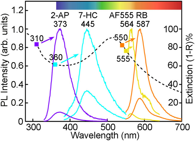
The bimetallic films are prepared by silver implantation (20 kV, 5 × 1016 cm−2). The dashed line shows the extinction spectrum of the bimetallic film and the excitation wavelengths for different fluorescence molecules are shown. The number on top of each curve shows the peak wavelength of the fluorescence emission spectrum. The enhancement factors are about 10, 3, 11, and 4 for 2-AP, 7-HC, AF555, and RB molecules.
The scanning electron microscopy (SEM) images of growing nano-island structure on our bimetallic film is depicted in Fig. 2 showing that the nano-islands are in the range of 20–30 nm. Image-Pro Plus version 6.0 is employed for the statistical analysis of the nano-islands. By adopting optimized metal ion implantation parameters and using high-purity Al foils that are cleaned and polished prior to silver ion implantation, periodically modulated structures are produced in the substrate. During ion implantation, heat is generated in the substrate and the aluminum surface softens thereby allowing plasmonic particle agglomeration to occur. The process can be divided into three stages based on the SEM images. A small amount of fuzzy protuberance is first formed on the planar surface after a fluence of 1.0 × 1016 cm−2 is implanted. The silver ions slowly upheave the surface and a disordered structure emerges. When the ion fluence reaches 5.0 × 1016 cm−2, the structure stabilizes and nano-islands are formed. The optical photographs in Fig. 2 shows the sample color changes obviously during the process, indicating there is a strong absorption induced by the nano-island structure.
Figure 2.
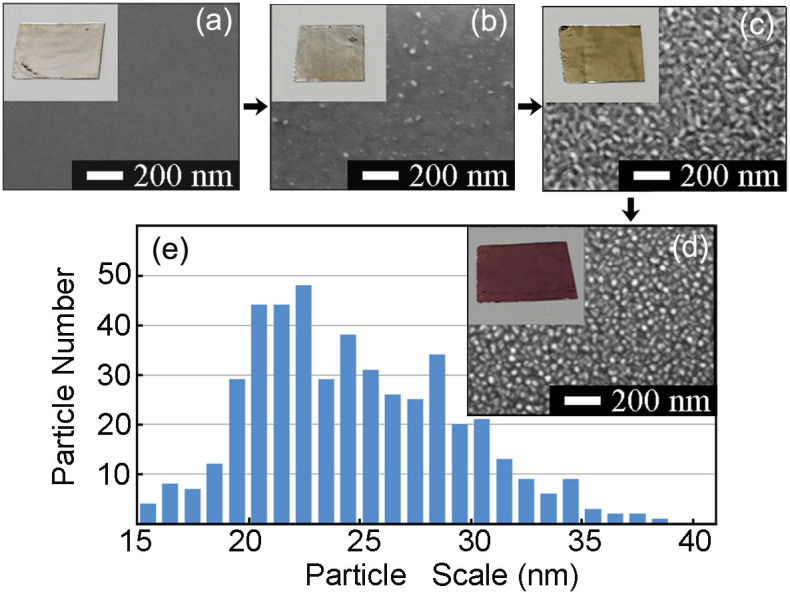
(a–d), SEM images and optical photographs of (a) untreated aluminum film and silver implanted aluminum films with different ion fluences of (b) 1 × 1016 cm−2, (c) 3 × 1016 cm−2, and (d) 5 × 1016 cm−2. (e), Statistical analysis of the nano-island distribution of (d).
The evolution of the UV–visible spectra is illustrated in Fig. 3(a). In the beginning, there is a strong major band in the UV range. As implantation proceeds, the major peak broadens and red-shifts due to the implanted silver ions. The silver peak at about 500 nm appears and when the ion fluence exceeds 5.0 × 1016 cm−2, there are no significant changes in the UV-Vis spectra. The accelerating voltage in the ion implantation experiments is 20 kV. Fluorescence signals of different dyes are measured on the films and the enhancement factors are shown in the insert of Fig. 3(a). The enhancement factors show different trends for dyes lie in different wavebands, verifying the enhancement is highly associated with the coupling between LSPR energy and fluorescence excitation energy, as discussed earlier. As the ion energy dominates the silver implantation depth and the effective distance of LSPR is supposed to be a limited value, the implantation voltage is an important parameter to obtain plasmonic structure. The influence of the accelerating voltage on the UV-Vis spectra is compared in Fig. 3(b) and more details about the influence of implantation parameters are shown in Fig. S2. The formation of the plasmonic substrate is induced by energetic metallic ion bombardment and this process is related to ion energy and ion size. The impact of silver ions changes with increasing accelerating voltage or larger silver layer depth. At very low energy, metal ions are likely deposited on the surface in lieu of implantation, as shown in Fig. S3. On the other hand, higher energy over 20 kV results in larger penetration depth and brings negative effects on LSPR properties. It should be noted that besides silver, other metallic ions can lead to the formation of plasmonic structures. For example, aluminum implanted aluminum films exhibits the UV plasmon band like the silver implanted aluminum films (see Fig. 2b). However, it is not as strong as that of the silver implanted films under the same experimental conditions. This is believed to be caused by the different mass of the ions and also the mean charge state of aluminum ions is smaller than that of silver38,39. All in all, our results show that a larger ion fluence produces a larger band shift and a higher accelerating voltage (penetrating depth) results in weakened plasmon resonance.
Figure 3. UV-visible spectra.
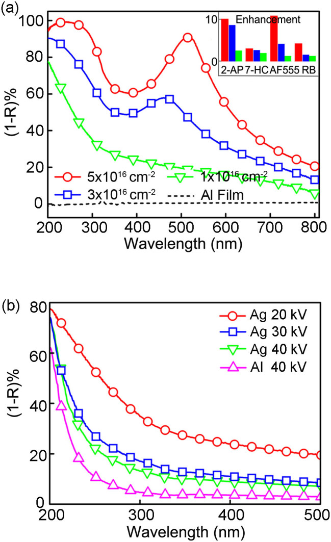
(a), untreated aluminum film and silver implanted aluminum films with ion fluences of 1 × 1016 cm−2, 3 × 1016 cm−2, and 5 × 1016 cm−2 at 20 kV. Insert shows fluorescence enhancement factor of different dyes on 1 × 1016 cm−2 (green), 3 × 1016 cm−2 (blue) and 5 × 1016 cm−2 (red) films. (b), silver implanted aluminum films at 20 kV, 30 kV and 40 kV and aluminum implanted aluminum film at 40 kV with ion fluencies of 1 × 1016 cm−2.
To evaluate the impact of the silver layers, X-ray photoelectron spectroscopy (XPS) and SRIM simulation are conducted to analyze the composition of the bimetallic films and the results are shown in Fig. 4 (Specific simulation data are available in Fig. S4). XPS shows the silver distribution at low ion fluences is in agreement to that predicted by SRIM. However, the peak shifts with silver ion fluence and it is caused by the formation of silver protuberances on the layer in accordance with the nano-island particles discussed previously. Hence, aggregation of silver ions may be responsible for the formation of the nano-island morphology.
Figure 4.
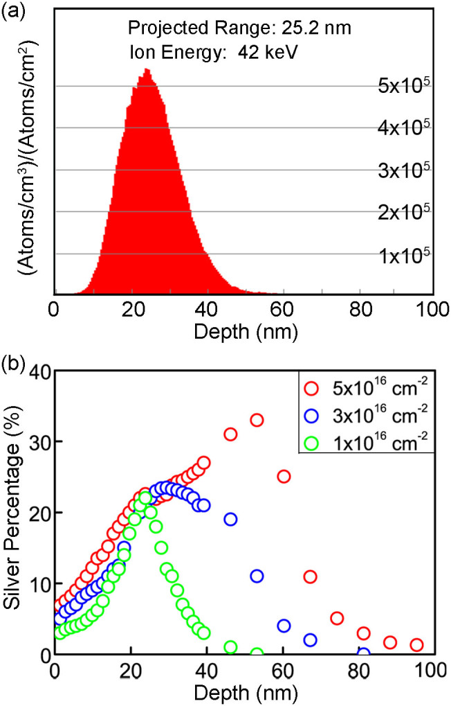
(a), Simulated ion ranges of the 20 kV silver implanted aluminum film. (b), XPS depth profile acquired from the silver implanted aluminum films with different ion fluences.
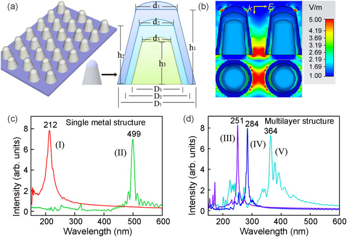
The finite-difference time-domain (FDTD) method is adopted to calculate the local electromagnetic field and monitor resonance frequency and the results are shown in Fig. 5. Fig. 5(a) shows a simple three-layer model for the FDTD simulation. A typical cross-sectional and planar view of the calculated radial EM field components of the nano-island structure is displayed in Fig. 5(b). The modes are excited by a broad band plane wave source from 150 nm to 1,500 nm perpendicular to the plane of the structure. The maximum local electric field is calculated to be 25.6 V m−1. The number of 25.6 cannot be simply regarded as the calculated enhancement for optical enhancement because the locally enhanced electric field not only accelerates the decay rate (lifetime reduction), but also increases the number of excitations per time. We then investigate the sensitivity of the plasmon resonance to variations of the diameters and heights of the three-layer structure. A reflection and transmission monitor is placed below the model (5 nm) to monitor plasmon resonance frequency. Incident light intensity is defined as one unit and the monitored EM field intensity below the model is shown in Fig. 5(c) and 5(d). The plasmonic properties of a single metal model is first investigated and Fig. 5(c) shows that the peak wavelength of LSPR is about 200 nm (I) and 500 nm (II) for pure aluminum and silver, respectively and they are in good agreement with our UV-Vis spectra data. The relationship between the LSPR properties of the multilayered structure of the bimetallic model and silver content is shown in Fig. 5(d). The LSPR spectrum gradually shifts to a longer wavelength and both the amount and depth of silver contribute to the shift. The shallow metal atoms contribute primarily to absorption in the bimetallic system. Comparison between curve II and curve IV in Fig. 5 shows that the surface metallic layer that is only 2% of the volume leads to a red-shift of 135 nm, suggesting that the LSPR frequency can be controlled by designing the plasmonic material. The simulation also shows that nano-particles with a fixed size can support only a few plasmonic modes but a large number of plasmonic modes are observed from the UV-Vis spectra band. This is because nano-island particles are embedded in the metal films and produce additional plasmonic modes that selectively couple to the nano-island plasmons to produce bonding and anti-bonding hybridized states.
Figure 5. FDTD simulation results of bimetallic nano-island models.
(a), Three-dimensional model of the nano-island structure. (b), Cross-sectional and planar views of the calculated radial EM field components of the multilayer nano-island structure with parameters D1 = 30 nm, D2 = 25 nm, D3 = 20 nm, d1 = 25 nm, d2 = 20 nm, d3 = 15 nm, h1 = 40 nm, h2 = 35 nm, and h3 = 30 nm. Height of the spherical cap is 5 nm and space between two particles is 10 nm. The inset in (b) shows the k-vector and polarization of the incident light. The 5-fold enhancement in the EM field is only artificially set to provide better intuitive models. (c), Calculated electric field intensity of a single metal aluminum model (I) and silver model (II). (d), Calculated electric field intensity of (III) Al-Ag-Al, (IV) Al-Ag-Ag models with fixed parameters in (b), and (V) Al-Ag-Ag with D2 = 30 nm, d2 = 20 nm with other parameters being fixed.
To conclude, the FDTD simulation demonstrates that the LSPR properties of the bimetallic system can be adjusted by changing the mixing ratio and layer thickness of the plasmonic composites and it can be readily accomplished by ion implantation. The bimetallic films reported here may have potential in other LSPR applications such as surface-enhanced Raman scattering40, photocatalysis41, photovoltaics42,43 and optical cloaking44.
Methods
Sample Preparation: Al films (99.99% pure, 0.2 mm thick) were degreased by acetone and electro-polished in a mixture of ethanol and perchloric acid with a volume ratio of 5:1 at a constant direct-current voltage of 15 V for 3 min to remove surface impurities. The polished aluminum films were rinsed in distilled water and dried. The HEMII-80 ion implanter (Plasma Technology Ltd.) equipped with a silver cathodic arc source was used to conduct ion implantation. The base pressure in the vacuum chamber was 5 × 10⁻⁴ Pa. The implantation parameters were all read off from the control panel on the instrument. Ion implantation was followed by the deposition a silica layer (5 nm) for samples used in fluorescence detection. This step served to protect the metal surface as well as adding a spacer layer between the metal surface and fluorophore. All samples were kept in vacuum environment after implantation process and were only exposed in the air when transferred. Surface oxidation is also not severe in this process, as shown in Fig. S5.
Characterization: 2-aminopurine (2-AP) and 7-hydroxycoumarin-3-carboxylic acid succinimidyl ester (7-HC) were purchased from Sigma-Aldrich and Alexa Fluor 555 (AF 555) and Rhodamine B (RB) were obtained from Invitrogen Molecular Probes. Quantum field information of AF 555 is obtained from the company document. The fluorescent molecules were dissolved separately in anhydrous ethanol to a concentration of about 10−6 mol L−1 and then spin coated on the sample surface (800 rpm for 8 s and then 3,000 rpm for 60 s, Laurell spin coater model WS-400BZ-6NPP-Lit). The photoluminescence spectral analysis was conducted on a Horiba Jobin-Yvon Fluorolog-3 spectrometer excited by a Xe lamp. XPS analysis with Al Ka irradiation was used to determine the chemical states and elemental depth profiles. The sputtering rate was estimated to be 1.4 nm min−1 in the first 30 minutes and 7 nm min−1 afterwards based on the rates calculated from a standard SiO2 film sputtered under the same conditions. The UV-visible spectra were acquired on a PerkinElmer LAMBDA750 spectrophotometer. Image-Pro Plus version 6.0 was used to conduct the statistical analysis of the nano-island scale and SRIM version 2010 was used to calculate the ion ranges.
Author Contributions
Q.H. and T.Q. conceived and coordinated the research. C.W., W.L. and H.H. contributed to the sample fabrication and synthesis. D.D. and J.L. contributed to the FDTD simulation. Q.H. and C.W. contributed to the optical tests. The manuscript was primarily written by Q.H. and revised by T.Q. and P.K.C. All authors contributed to discussions and manuscript review.
Supplementary Material
SUPPLEMENTARY INFO
Acknowledgments
This work was jointly supported by the National Natural Science Foundation of China under Grant No. 51271057, the Natural Science Foundation of Jiangsu Province, China, under Grant No. BK2012757, the Program for New Century Excellent Talents in University of Ministry of Education of China under Grant No. NCET-11-0096, Research and Innovation Project for College Graduates of Jiangsu Province No. KYZZ_0064, Hong Kong Research Grants Council (RGC) General Research Funds No. 112510 and Guangdong - Hong Kong Technology Cooperation Funding Scheme (TCFS) GHP/015/12SZ.
References
- Fort E. & Grésillon S. Surface enhanced fluorescence. J. Phys. D Appl. Phys. 41, 013001 (2008). [Google Scholar]
- Murray W. A. & Barnes W. L. Plasmonic materials. Adv. Mater. 19, 3771–3782 (2007). [Google Scholar]
- Jensen T. R., Malinsky M. D., Haynes C. L. & Van Duyne R. P. Nanosphere lithography: tunable localized surface plasmon resonance spectra of silver nanoparticles. J. Phys. Chem. B 104, 10549–10556 (2000). [Google Scholar]
- Evanoff D. D. & Chumanov G. Synthesis and optical properties of silver nanoparticles and arrays. Chemphyschem 6, 1221–1231 (2005). [DOI] [PubMed] [Google Scholar]
- Jain P. K., Huang X., El-Sayed I. H. & El-Sayed M. A. Review of some interesting surface plasmon resonance-enhanced properties of noble metal nanoparticles and their applications to biosystems. Plasmonics 2, 107–118 (2007). [Google Scholar]
- Ray K., Chowdhury M. H. & Lakowicz J. R. Aluminum nanostructured films as substrates for enhanced fluorescence in the ultraviolet-blue spectral region. Anal. Chem. 79, 6480–6487 (2007). [DOI] [PMC free article] [PubMed] [Google Scholar]
- Chan G. H., Zhao J., Schatz G. C. & Duyne R. P. V. Localized surface plasmon resonance spectroscopy of triangular aluminum nanoparticles. J. Phys. Chem. C 112, 13958–13963 (2008). [Google Scholar]
- Jha S. K., Ahmed Z., Agio M., Ekinci Y. & Löffler J. F. Deep-UV surface-enhanced resonance Raman scattering of adenine on aluminum nanoparticle arrays. J. Am. Chem. Soc. 134, 1966–1969 (2012). [DOI] [PubMed] [Google Scholar]
- Sigle D. O., Perkins E., Baumberg J. J. & Mahajan S. Reproducible Deep-UV SERRS on Aluminum Nanovoids. J. Phys. Chem. Lett. 4, 1449–1452 (2013). [DOI] [PubMed] [Google Scholar]
- Ekinci Y., Solak H. & Löffler J. Plasmon resonances of aluminum nanoparticles and nanorods. J. Appl. Phys. 104, 083107 (2008). [Google Scholar]
- Knight M. W. et al. Aluminum plasmonic nanoantennas. Nano Lett. 12, 6000–6004 (2012). [DOI] [PubMed] [Google Scholar]
- Tam F., Goodrich G. P., Johnson B. R. & Halas N. J. Plasmonic enhancement of molecular fluorescence. Nano Lett. 7, 496–501 (2007). [DOI] [PubMed] [Google Scholar]
- Wilson R. The use of gold nanoparticles in diagnostics and detection. Chem. Soc. Rev. 37, 2028–2045 (2008). [DOI] [PubMed] [Google Scholar]
- Holzmeister P., Acuna G. P., Grohmann D. & Tinnefeld P. Breaking the concentration limit of optical single-molecule detection. Chem. Soc. Rev. 43, 1014–1028 (2014). [DOI] [PubMed] [Google Scholar]
- Lakowicz J. R. Radiative decay engineering: biophysical and biomedical applications. Anal. Biochem. 298, 1–24 (2001). [DOI] [PMC free article] [PubMed] [Google Scholar]
- Loo C., Lowery A., Halas N., West J. & Drezek R. Immunotargeted nanoshells for integrated cancer imaging and therapy. Nano Lett. 5, 709–711 (2005). [DOI] [PubMed] [Google Scholar]
- Hao Q., Qiu T. & Chu P. K. Surfaced-enhanced cellular fluorescence imaging. Prog. Surf. Sci. 87, 23–45 (2012). [Google Scholar]
- Willets K. A. & Van Duyne R. P. Localized surface plasmon resonance spectroscopy and sensing. Annu. Rev. Phys. Chem. 58, 267–297 (2007). [DOI] [PubMed] [Google Scholar]
- Blaber M. G., Arnold M. D. & Ford M. J. A review of the optical properties of alloys and intermetallics for plasmonics. J. Phys.: Condens. Mat. 22, 143201 (2010). [DOI] [PubMed] [Google Scholar]
- Maier S. A. & Atwater H. A. Plasmonics: Localization and guiding of electromagnetic energy in metal/dielectric structures. J. Appl. Phys. 98, 011101 (2005). [Google Scholar]
- Prodan E., Radloff C., Halas N. & Nordlander P. A hybridization model for the plasmon response of complex nanostructures. Science 302, 419–422 (2003). [DOI] [PubMed] [Google Scholar]
- Hao E. & Schatz G. C. Electromagnetic fields around silver nanoparticles and dimers. J. Chem. Phys. 120, 357–366 (2003). [DOI] [PubMed] [Google Scholar]
- Hutter E. & Fendler J. H. Exploitation of localized surface plasmon resonance. Adv. Mater. 16, 1685–1706 (2004). [Google Scholar]
- Cortie M. B. & McDonagh A. M. Synthesis and optical properties of hybrid and alloy plasmonic nanoparticles. Chem. Rev. 111, 3713–3735 (2011). [DOI] [PubMed] [Google Scholar]
- Bai C. & Liu M. Implantation of nanomaterials and nanostructures on surface and their applications. Nano Today 7, 258–281 (2012). [Google Scholar]
- Chu P. K., Chen J., Wang L. & Huang N. Plasma-surface modification of biomaterials. Mater. Sci. Eng. R. 36, 143–206 (2002). [Google Scholar]
- dos Santos Claro P. C. et al. Spontaneous nanoripple formation on metallic templates. ACS Nano 2, 2531–2539 (2008). [DOI] [PubMed] [Google Scholar]
- Wang J., Jia G., Mu X. & Liu C. Quasi-two-dimensional Ag nanoparticle formation in silica by Xe ion irradiation and subsequent Ag ion implantation. Appl. Phys. Lett. 102, 133102 (2013). [Google Scholar]
- Carles R. et al. The synthesis of single layers of Ag nanocrystals by ultra-low-energy ion implantation for large-scale plasmonic structures. Nanotechnology 20, 355305 (2009). [DOI] [PubMed] [Google Scholar]
- Carles R. et al. Three Dimensional Design of Silver Nanoparticle Assemblies Embedded in Dielectrics for Raman Spectroscopy Enhancement and Dark-Field Imaging. ACS Nano 5, 8774–8782 (2011). [DOI] [PubMed] [Google Scholar]
- Wilhelmsson L. M. Fluorescent nucleic acid base analogues. Q. Rev. Biophys. 43, 159–183 (2010). [DOI] [PubMed] [Google Scholar]
- Setsukinai K.-i., Urano Y., Kikuchi K., Higuchi T. & Nagano T. Fluorescence switching by O-dearylation of 7-aryloxycoumarins. Development of novel fluorescence probes to detect reactive oxygen species with high selectivity. J. Chem. Soc., Perkin Trans. 2, 2453–2457 (2000). [Google Scholar]
- Magde D., Rojas G. E. & Seybold P. G. Solvent dependence of the fluorescence lifetimes of xanthene dyes. Photochem. Photobiol. 70, 737–744 (1999). [Google Scholar]
- Qiu T. et al. High-sensitivity and stable cellular fluorescence imaging by patterned silver nanocap arrays. Acs Appl. Mater. Inter. 2, 2465–2470 (2010). [DOI] [PubMed] [Google Scholar]
- Novotny L. & van Hulst N. Antennas for light. Nature Photonics 5, 83–90 (2011). [Google Scholar]
- Lakowicz J. R. et al. Radiative decay engineering: 2. Effects of silver island films on fluorescence intensity, lifetimes, and resonance energy transfer. Anal. Biochem. 301, 261–277 (2002). [DOI] [PMC free article] [PubMed] [Google Scholar]
- Akbay N., Lakowicz J. R. & Ray K. Distance-dependent metal-enhanced intrinsic fluorescence of proteins using polyelectrolyte layer-by-layer assembly and aluminum nanoparticles. J. Phys. Chem. C 116, 10766–10773 (2012). [DOI] [PMC free article] [PubMed] [Google Scholar]
- Brown I. G. Vacuum arc ion sources. Rev. Sci. Instrum. 65, 3061–3081 (1994). [Google Scholar]
- Yushkov G. Y., Anders A., Oks E. M. & Brown I. G. Ion velocities in vacuum arc plasmas. J. Appl. Phys. 88, 5618–5622 (2000). [Google Scholar]
- Dörfer T., Schmitt M. & Popp J. Deep-UV surface-enhanced Raman scattering. J. Raman Spectrosc. 38, 1379–1382 (2007). [Google Scholar]
- Damato T. C., de Oliveira C. C., Ando R. A. & Camargo P. H. A Facile Approach to TiO2 Colloidal Spheres Decorated with Au Nanoparticles Displaying Well-Defined Sizes and Uniform Dispersion. Langmuir 29, 1642–1649 (2013). [DOI] [PubMed] [Google Scholar]
- Mihi A., Beck F. J., Lasanta T., Rath A. K. & Konstantatos G. Imprinted Electrodes for Enhanced Light Trapping in Solution Processed Solar Cells. Adv. Mater. 26, 443–448 (2014). [DOI] [PubMed] [Google Scholar]
- Atwater H. A. & Polman A. Plasmonics for improved photovoltaic devices. Nature Mater. 9, 205–213 (2010). [DOI] [PubMed] [Google Scholar]
- Cai W., Chettiar U. K., Kildishev A. V. & Shalaev V. M. Optical cloaking with metamaterials. Nature photonics 1, 224–227 (2007). [Google Scholar]
Associated Data
This section collects any data citations, data availability statements, or supplementary materials included in this article.
Supplementary Materials
SUPPLEMENTARY INFO


