

Abstract
The structural order in ultrathin films of monolayer protected clusters (MPCs) is important in a number of application areas but can be difficult to demonstrate by conventional methods, particularly when the metallic core dimension, d, is in the intermediate size-range, 1.5 < d < 5.0 nm. Here, improved techniques for the synthesis of monodisperse thiolate-protected gold nanoparticles have made possible the production of dodecane-thiolate saturated ~ 4 ± 0.5 nm Au clusters with single-crystal core structure and morphology. An ultrathin ordered film or superlattice of these nanocrystal-core MPCs is prepared and investigated using aberration corrected scanning/transmission electron microscopy (STEM) which allowed imaging of long-range hexagonally ordered superlattices of the nanocrystals, separated by the thiolate groups. The lattice constants determined by direct imaging are in good agreement with those determined by small-angle electron diffraction. The STEM image revealed the characteristic grain boundary (GB) with sigma (Σ) 13 in the interface between two crystals. The formation and structures found are interpreted on the basis of theoretical calculations employing molecular dynamics (MD) simulations and coarse-grained (CG) approach.
Keywords: Monolayer protected clusters (MPCs), thiolates, gold nanocrystals or nanoparticles, Superlattices, long range ordered, MD simulations, coarse grained approach, grain boundary
1. Introduction
Ordered ultrathin films of protected metallic nanoparticles are of interest for various applications, one of which is their utility in single-nanoparticle structure determination. Structure determination at the nanoscale is challenging because of the variety of materials interfaces that may be present, i.e. interactions with substrate or supports, with adsorbates, or ligands. Monolayer protected clusters (MPCs) are a class of nanoparticles in which a metallic core is encapsulated by a complete shell of strongly adsorbed ligands, such as thiolates (RS-). They behave in many ways like single macromolecules that share a similar dimension and tail-group (R) functionality. Samples of MPCs are typically characterized en masse — as opposed to single-particle measurements — but this involves averaging over the inhomogeneities of size, shape, and internal structure that are present in the as-prepared samples.1 Advances in instrumentation for high-resolution electron microscopy (STEM) and selected-area electron diffraction (ED) offer the possibility to rapidly determine the key structural characteristics of such assemblies, based on single-molecule measurements.2 Such measurements must contend with the inherent mobility, both orientational and translational, of the MPCs on the transmission electron microscopy (TEM) substrates. Also there is the need to collect the structure-relevant information on each targeted MPC prior to beam damage, to which the thiolate sulfur-carbon (S-C) bond is particularly susceptible.
One way to improve such measurements is to prepare ultrathin ordered films of the MPCs. The spatial regularity and high lateral (in-plane) density of such films facilitate the rapid sequential measurement of numerous MPCs. In such films the immobility of single MPCs results from the same weak dispersion-dominated forces that result in crystallization of ordered 3D-arrays of MPCs. The film-formation process may be similar to crystallization from solution, which itself acts to accomplish segregation by size, improving the homogeneity of a given superlattice domain or platelet crystallite. Of course it can be challenging to prepare ultrathin ordered films with substantial regions of the preferred trilayer thickness. But several advances have occurred in recent years, cf. the reports from the groups of Jaeger,3, 4 Yacaman,5-7 Kagan and Murray,8-10 Talapin,11, 12 Landman and Leudtke,13 Pileni,14 and Whetten et al.15. The superlattice formation has been attributed to oriented attachment phenomena, 16-19 and atomic binding of specific crystal facets.16, 20 Recently, Mezour et al. have proposed a self-assembled molecular network as the template for Au NP assemblies at the liquid–solid interface.21 The methods used in these reports have worked on samples of larger nanocrystals, typically much greater than 4-nm core dimension. In most reports the emphasis is mainly on issues other than structure determination.
Computer simulations in combination with crystallographic analysis in scanning transmission electron microscopy (STEM) provide valuable tools for understanding the formation of such superlattices. In this sense, systematic investigation of the nanoparticle assembly processes by matching simulation and experiment can help interpret fundamental physical interactions and processes. The huge number of particles involved in the formation of colloidal superlattices means that atomistic simulations become infeasible to apply. By contrast, coarse-grained (CG) approaches have been used in recent years to simulated different colloidal systems. For instance, Jia-Qi Lin22 has used CG molecular dynamics (MD) simulations to investigate the dynamics of gold monolayer-protected clusters (MPCs) in solvents. Cheng et al.23 used a GC approach to study the assembly of gold MPCs in a solution, induced by solvent evaporation.
Here we report on new structure-determination results obtained via STEM imaging and electron diffraction on the classic system of ~ 4-nm gold (Au) nanocrystals protected by a monolayer of dodecane-thiolate (ddt) ligands. Both the formation of the superlattice and its structural characteristics using TEM/STEM are supported by MD and CG models. The typical grain boundary present between two crystals is also explained. This system is important, in its own right, but our prime emphasis here is to explore the factors that might limit application of the ultrathin-film TEM-based method, with a view toward extending it ultimately to the sub-3.0 nm regime.
2. Experimental
2.1 Synthesis
2.1.1 Materials
The various chemicals: chloroauric acid (HAuCl4.6H2O), tetraoctylammonium bromide (TOA-Br, 98%), 1-dodecanethiol (ddt, 98%), sodium borohydride (NaBH4), were purchased from Sigma Aldrich and used as received, along with solvents toluene and deionized water.
2.1.2 MPC synthesis
Au MPCs were synthesized by modified Brust’s method from the phase transfer of metal in aqueous phase to organic phase.24 Aqueous HAuCl4 (1.0 mL, 50 mM) was thoroughly mixed with 10 mL toluene. Into this solution, 0.2737 gm of TOA-Br was added and continued stirring producing orange color indicating the transfer of Au(III) from aqueous to organic phases by the formation of Oct4N+AuBr4-. An hour later, 0.03 mL (30 μL) of ddt was added to the stirred solution to form a colorless product indicative of Au(I)-thiolate oligomers. After 30 minutes, 6.25 mL of ice chilled NaBH4 (0.25 M) was added drop-wise in such a way that all the reaction will be completed in the presence of NaBH4. The change from colorless to opaque black indicated the formation of metallic MPCs. The reaction mixture was left undisturbed for six hours of continuous stirring, sufficient that all the NaBH4 will be consumed. During the reaction process, TOA-Br acts as the phase-transfer catalyst and the solubilizing agent and BH4 anion as the reducing agent and the resulting MPCs will be protected by ddt groups. The sample was left undisturbed for two days and then the toluene-soluble product MPCs were separated from aqueous phases and were repeatedly washed of by-products by precipitation using added ethanol and then preserved in a refrigerator.
2.1.3 Superlattice (SL) Formation
The superlattice (SL) was fabricated using a solution of monodisperse ddt protected Au MPCs following the procedure reported by Bigioni et al.4 In this procedure, a small quantity of excess ddt ligand was added to the highly concentrated toluene solution, which was then drop-cast on a carbon-coated S/TEM grid and covered with a watch-glass overnight for slow evaporation. The presence of excess ligands and slow evaporation retards the crystal growth to achieve quasi-reversible thin-film formation at the liquid-vapor interface, followed by settling onto the substrate (carbon coated copper grid). This process and a model to account for its results are described in great detail in Bigioni et al. 4
2.2 Electron Microscopy Characterization
TEM images and selected area electron diffraction patterns were obtained in a JEOL 2010-F TEM operated at 200 kV. Diffraction patterns were recorded at varying camera length(s) from 20 cm to 200 cm. STEM images were recorded in a probe Cs-corrected JEOL JEM-ARM 200F operated at 80 kV with both dark field and bright field detectors. High angle annular dark field (HAADF) STEM images were obtained with a convergence angle of 26 mrad and the collection semi-angles from 50 to 180 mrad.
3. Results and Discussion
The shape, size and crystalline structure of the MPC’s metallic core are investigated using TEM operated at 200 kV. The imaging of thiolated NPs is quite challenging and getting high resolution images is complicated. For SL formation, each particle should behave as the molecule and should self-assemble against all other forces so that an ordered array of atoms will be obtained. However, the thiolate groups present in the MPCs can lubricate the interface giving NPs a high mobility. The presence of excess thiols from the MPC makes electron microscopy imaging very difficult and the interaction of electron beam with thiolate contaminates the sample reducing the resolution and the problem can be overcome by reducing the voltage and also minimizing the imaging time.2, 25 Even the use of low voltage for short period of time can produce the coalescence of the particles and new larger particle might be formed.
An example of a TEM image of the well-ordered SL is presented in the Figure 1. The low resolution TEM images showing the micron sized particle is presented in Figure S1 of supporting information (SI). The domain size of SL depends on the solution concentration of the MPCs. For lower concentration, smaller domains are formed, while for higher concentration the larger domains are produced and in some cases superposition of different domains will be obtained. In higher concentration cases, the interaction between particles increases, thereby increasing the pinning effect and isolating the de-wetting holes, forming more compact monolayer where the entropy driven self-assembly becomes effective.26 The electron microscopy images showed many features that resemble the conventional atomic and molecular crystals. Our analyses show, see Figure 1, that most of the particles are aligned along same orientation. According to our best analysis, many of the particles (the nanocrystal cores) appear to be aligned with the [111] vector normal to the film, i.e. aligned along the viewing axis. Otherwise they are not oriented with respect to one another. This is also indicated by the SAED pattern (Figure 1b), which shows the Bragg reflections (bright spots) are distributed rather uniformly around the rings, as in powder-pattern diffraction.
Figure 1.
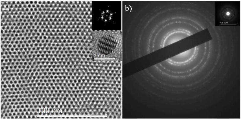
TEM image and diffraction pattern of 4 ± 0.5 nm sized Au superlattice. a) TEM image showing the long range ordered Au nanocrystal. The FFT patterns of the SL and HRTEM image of representative nanostructure is inset in the Figure a where the single crystal nature is observed and most of the MPCs are in the same orientation. b) Selected area diffraction pattern for SL obtained using 20 cm camera length with several diffraction rings. The inset in Figure b represents the diffraction pattern obtained using 200 cm camera length revealing the overall crystalline structure of the SL to be hexagonally packed long range order. More examples are presented in SI (Figure S2). The FFT pattern inset in frame a and diffraction pattern inset in frame b are in good agreements and shows that the SL is long range ordered hexagonally packed.
The magnified image shows that the particles have well defined dimensions and morphology. The cores are typically identified as 4.0 ± 0.5 nm diameter FCC single crystallites of truncated octahedron (TO) morphology, that exposes 6 {100} and 8 {111} facets. The fast Fourier transform (FFT) patterns of the SL showed the single crystal nature of the whole crystal. In addition, the crystalline structure of the superlattice was investigated using selected area diffraction patterns and is presented in Figure 1b. The diffraction pattern presents several possible rings indicating the presence of FCC crystalline structure. The camera length of TEM was increased to 200 cm; the diffraction pattern at high camera length is similar to small angle electron diffraction, interestingly, hexagonal ordered diffraction pattern is obtained in the center of the diffraction pattern (see inset in Figure 1b and Figure S2 in SI). The average angles measured between nearby reflection point is found to be (60 ± 1)°, (59 ± 1)° and (61 ± 1)° refers to the hexagonally ordered system. In addition the distance between two reflection points is ~ 6.1 nm which is in agreement with the distance from FFT pattern. This distance refers to the average distance between two Au MPCs. For better accuracy, more than 20 diffraction patterns were recorded at different areas of the superlattice and an average value is taken. It is important to note that despite several factors (particle-particle and particle–substrates interaction, van der Waals interaction, dipole-diploe interaction, coulomb interaction and maximization of entropy), the SL presents long-range order, which is the most important characteristic for the applications of SL in practical purposes.
In addition to TEM imaging at 200 kV, we reduced the voltage to 80 kV for STEM imaging and also cleaned the sample prior to imaging as reported in our previous report.2 The low magnification SL imaging using STEM is presented in Figure 2a, where the SL comprises three domains, as shown in inset FFT marked by the numerals 1, 2 and 3. The angle between two reflection points 1 and 2 (SL domains 1 and 2) is 13 ± 1° and 1 and 3 (SL domains 1 and 3) is 31 ± 1°. Hence, it can be inferred that the SL domain 2 and 3 are rotated by angles 13 ± 1° and 30 ± 1°, respectively, with respect to SL domain 1. The contribution from each SL plane is presented in Figure 2b (lattice 1), Figure 2c (lattice 2) and Figure 3c (lattice 3) with the corresponding FFT pattern inset on it. An elaborated image is presented in S3 in SI. The S atoms from thiolate adsorbed head group are uniformly distributed along the facets of the nanocrystals. The distance between nanocrystal pairs also changes according to the vertical, horizontal or diagonal direction. An average distance is estimated by measuring the distance between 20 Au MPCs for each diagonal, horizontal and vertical case and is presented in the Figure 2e, where the distance between 20 Au MPCs is shown. The average distance between two Au MPCs is found to be 6.20 ± 0.14 nm in diagonal case while 6.17 ± 0.14 nm in vertical case. However, the distances measured locally differ from the average distance in some cases. The intensity line profiles traced along vertical and horizontal directions, show the variation in the intensities of the peak revealing the anisotropy in the crystal, with higher degree of ordering in the vertical direction and a lower degree of ordering horizontally.27 In addition, the average distance for thiolate molecules in diagonal direction was 1.95 ± 0.14 nm and for vertical and horizontal direction was 1.85 ± 0.14 nm. Hence, the average interparticle distance for diagonal case is relatively larger than for horizontal or vertical case. This distance and face-to-face assembly of MPCs shows the interdigitation or bundling of thiolate molecules between the surfaces of two nearby MPCs.28-31 Clearly, gold MPC superlattices present excellent long-range order as seen from electron micrographs. The average distances between two MPCs obtained from high resolution STEM images are in close agreement with the distance obtained from diffraction patterns. On the other hand, the interaction between electron beam and nanoparticles, in high vacuum, inside the microscope produces the coalescence of particles.32 The real coalescence phenomena are presented in Figure S4 in SI as seen under TEM. Initially, almost all the particles were single crystal, however, as the time passes, the ligands separating them will be destroyed and the combination of nearby cores takes place producing the larger particles (as presented in Figure S4, left and right).
Figure 2.
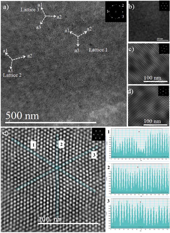
a) Low magnification STEM image of Au MPC superlattice. The fast Fourier transform (FFT) pattern is inserted in the top of the image and shows six (6) strong reflection points denoted by 1 and 12 weak reflection points denoted by 2 and 3. The strong and weak reflection suggests the superlattice is made from the three lattice domains oriented along distinct directions. The magnified portion of the lattices are presented in figure b (lattice 1), figure c (lattice 2) and figure d (lattice 3). The direction for the lattice vectors a1, a2 and a3 is inserted in each lattice. The average angle measured between lattice 1 and lattice 2 is (13 ± 1)° and lattice 1 and lattice 3 is (30 ± 1)°, inferring that lattice 2 is rotated from lattice 1 by an angle of (13 ± 1)° and lattice 3 is rotated by an angle of (30 ± 1)°. e) A magnified portion of STEM images in lattice 1 for the statistics of distance between two MPCs. Three different directions are marked by 1, 2 and 3 and the intensity profile for corresponding direction is presented in the right panel and labelled as 1, 2 and 3. The average distance is obtained from the average between 20 values, the average distance along direction 1 is 6.3 nm, and direction 2 is: 6.06 nm and along direction 3 is: 6.17 nm. The FFT is inset in all cases.
Figure 3.
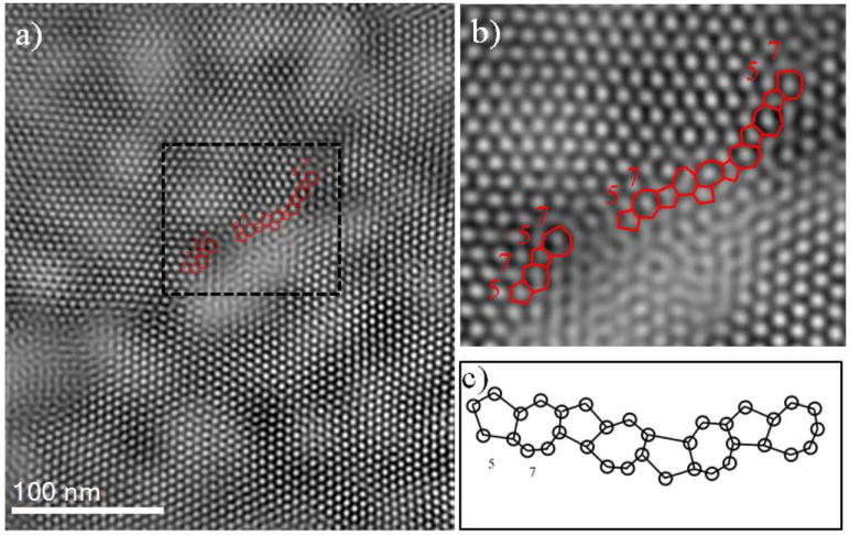
Grain boundary interpretation in the interface between lattice 1 and lattice 3. a) Typical STEM image in the interface between lattice 1 and lattice 3. The rectangular region is chosen in the interface and magnified image of the selected region is presented in (b), where a regular sequences of atomic rings of 57 is observed. The GB with the sequence of atomic rings of 57 corresponds to sigma (Σ) = 13. c) Schematic of the atomic model for structural units with atomic rings (57).
The presence of defects in the interface region between the crystals plays an important role as the crystal growth can be altered in the expense of another crystal and directly affects the physical and mechanical properties of SLs.33 The structural defects can be estimated from coincidence-site lattice (CSL) and the structure units.34, 35 An example of CSL is presented in Figure 3a, where the atomic rings can be counted in the interface region between lattice 1 and lattice 2. A more magnified image of the interface is presented in figure 3b, where a sequence of atomic rings (57) are observed from the high resolution STEM images which corresponds to GB equivalent to Sigma (Σ) = 13 or complementary Σ = 31, where Σ is the ratio of CSL sites to lattice sites of one of the crystals and mostly is present from the rotation about the low index direction. The schematic of the atomic model for structural units with the sequence of images with atomic rings (57) is presented in figure 3c.
Theoretical calculations
Atomistic simulations – NP-NP distances
In order understand the origin of the inter-particle distances observed experimentally, we have performed full atomistic simulations using molecular dynamics with a Langevin thermostat. Two truncated octahedral Au nanocrystals composed of 1289 atoms each, were firstly passivated with 1-dodecanethiol with the same methodology as in reference. 36 Thereafter, they were slowly approaching in steps of 0.2 Å. At each step, 50 ps of Langevin dynamics at 300 K were performed, with a friction coefficient of 50 ps-1. The NP-NP distance is defined as the shorter distance between the most peripherical atoms in the contact line direction. At each approaching step the internal energy of the system is computed using the interatomic potential of reference.36
Au-Au interactions were simulated under the Second Moment approximation of the Tight-Binding (SMTB);37 which takes into account the many-body character of the metallic bonds. Intra- and intermolecular interactions of ligands were simulated under the Universal Force Field38 approximation within the united atom method, using the same potential parameters as reported in reference.36 These interactions consist on bond stretching; bond bending, torsional and dispersion forces. For the last ones a cut-off of one nanometer was used. For the S-Au we have employed the bond-order Morse potential developed by Olmos-Asar et.al.36
A plot of the internal energy as a function of the NP-NP distance is shown in Figure 4. As observed in the Figure, while the NPs approach each other, the internal energy decreases mainly due to the van der Waals interaction between alkyl chains. It should be noted at this point, that the length of one dodecanethiol molecule is close to 15 Å (i.e. with all trans configurations), so we expect a priori a NP-NP distance of 30 Å. However, as shown in the plot three defined minima were observed at approximately 22, 18 and 12 Å, which clearly demonstrate the interdigitation of the alkyl chains. Therefore, one should expect from the theoretical calculations NP-NP distances between 12 and 22 Å. The high resolution TEM image taken in a magnified region showed exactly these ranges of distances.
Figure 4.
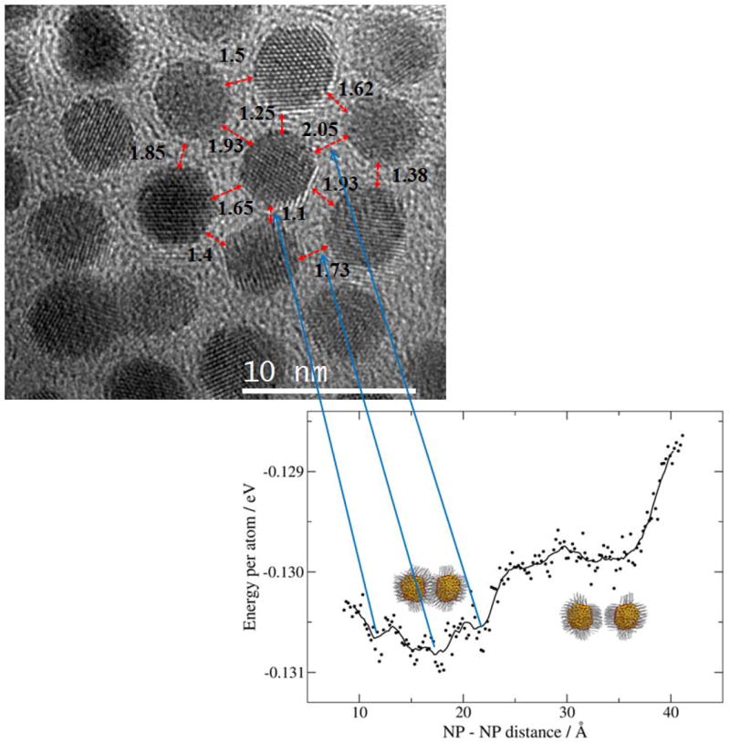
Top: high resolution TEM image of the 2D Au NP superlattice showing the experimentally NP-NP distances in nm. Lower: Atomistic simulations showing the internal energy as a function of the NP-NP distance. The minimum corresponds to most stable configurations.
Coarse grained simulations- lattice formation
We have also modeled the monolayer protected gold nanoparticles by a coarse grained approach due to the fact that full atomistic simulations of the assembly process are unpractical from a computation cost. The NP-NP interaction was represented within this approach by the Everaers potential,39 which results from describing each nanoparticle as an integrated collection of Lennard-Jones particles of size σ, and contains both attractive and repulsive components. The colloid-colloid interaction VNP-NP is given by:
Where ANP–NP = 39.48ɛ is the Hamaker constant for the NP-NP interaction and a1 and a2 the radii of the two colloidal nanoparticles, which in the present case a1 = a2 = 2 nm. The colloid-solvent interaction energy, VNP–Sol , is derived from VNP-NP(r), by letting the size of one of the particles go to zero:
Where ANP–Sol , is the Hamaker constant for the NP-Solvent interaction and a the radii of the Au nanoparticle. The solvent-solvent interaction is represented by a Lennard-Jones potential with a Hamaker constant ASol–Sol.= 144 .
All simulations were performed using the LAMMPS code,40. The Nose-Hoover thermostat has been used to integrate equations of motion under the NPT ensemble. Initially a 2D random distribution of Au nanoparticles is placed in the simulations box with different concentration of solvent trapped. The initial temperature was held fixed at 4.0 ɛ/kB and subsequently decreased until 0.01 ɛ / kB in order to obtain lower energy configurations.
In Figure 5, the final configurations after 10×106 MD steps are shown. In Fig 5a a well-ordered 2D superlattice of Au nanoparticles is observed. Close inspection (see inset of Fiure 5a) shows a hexagonal arrangement of Au NPs. However grain-boundaries as well as vacancies in the superlattice are evident, in excellent agreement with the experimental images showed above (see Figure 2). The amount of solvent particles was varied from 10 to 90 % during the superlattice formation and in general terms the same qualitative results are obtained. For instance, in Figure 5b a superlattice of Au nanoparticles with 90% of solvent trapped is shown. The same kind of grain boundary, separating two domains of the nanocrystals, is observed, indicating that the solvent trapped during the evaporation step does not play a relevant role.
Figure 5.
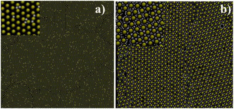
2D Au NP superlattices obtained after minimization, using the coarse-grained approach, a) with 10 % of solvent trapped during superlattice formation. b) with 90 % of solvent trapped. Yellow spheres: Au NPs, White (small) spheres: solvent particles.
4. Summary and Conclusion
In conclusion, we have synthesized well controlled Au NPs with sizes 4 ± 0.5 nm and single crystal in nature using modified Brust’s method. The superlattice film is prepared by drop casting method in carbon film and studied using TEM and STEM. The electron microscopy images revealed some interesting properties of SL formation with long-range order and the presence of some local disorder in the grain boundary and also in the surface. The diffraction pattern obtained at high camera length showed the hexagonal ordering of the Au MPCs, interestingly the distance is in agreement with the distance between two Au MPCs in high resolution STEM images. Face to face assembling of single crystal with interdigitated/bundeled thiolate groups is observed. The high resolution STEM images in the interface between two crystals suggested the GB equivalent to Sigma (Σ) = 13. Computer simulations at different level of theory were employed to characterize and explain the experimental evidence. In particular we have confirmed by means of atomistic simulations the interdigitation of the alkyl chains with NP-NP distances in the range between 12 and 22 Å, values considered lower than the combined lengths of two dodecanethiolate groups (i.e. 30 Å). Separately, using a coarse grained approach we were able to reproduce the formation of 2D superlattice of Au NPs that resemble very well the experimental ones. In particular one finds the formation of short-range well defined structures separated by grain boundaries as well as the existence of vacancies and imperfections in the superlattice. The last simulations constitute a motivation to further research in order to determine optimal conditions to obtain perfect defect-free superlattices. This progress at the level of 4-nm diameter particles will be an important for future work aimed at preparing large-area ultrathin crystalline films of uniform sub-3-nm metallic cores for applications in optics, electronics, sensing and many more.
Supplementary Material
Acknowledgments
This project was supported by grants from the National Center for Research Resources (5 G12RR013646-12) and the National Institute on Minority Health and Health Disparities (G12MD007591) from the National Institutes of Health. The authors would like to acknowledge to the NSF for support with grants DMR-1103730, “Alloys at the Nanoscale: The Case of Nanoparticles Second Phase and PREM: NSF PREM Grant # DMR 0934218; “Oxide and Metal Nanoparticles- The Interface Between Life Sciences and Physical Sciences”. In addition, the authors would like to acknowledge the support of the Welch Foundation (grant No. AX-1615, “Controlling the Shape and Particles Using Wet Chemistry Methods: The Case of Bimetallic Nanoparticles”. MMM wish to thank CONICET, Universidad Nacional de Córdoba, ANPCyT Program BID (PICT 2010-123), PIP: 112-200801-000983 “Nanotechnology in-silico” for financial support.
Footnotes
Supporting Information
Low magnification TEM image, superlattice diffraction using 200 cm camera length, TEM images for coalescence is presented in supporting information.
Notes and References
- 1.Billinge SJ, Levin I. Science. 2007;316:561–565. doi: 10.1126/science.1135080. [DOI] [PubMed] [Google Scholar]
- 2.Bahena D, Bhattarai N, Santiago U, Tlahuice A, Ponce A, Bach SBH, Yoon B, Whetten RL, Landman U, Jose-Yacaman M. J Phys Chem Lett. 2013;4:975–981. doi: 10.1021/jz400111d. [DOI] [PMC free article] [PubMed] [Google Scholar]
- 3.Mueggenburg KE, Lin X-M, Goldsmith RH, Jaeger HM. Nat Mater. 2007;6:656–660. doi: 10.1038/nmat1965. [DOI] [PubMed] [Google Scholar]
- 4.Bigioni TP, Lin X-M, Nguyen TT, Corwin EI, Witten TA, Jaeger HM. Nat Mater. 2006;5:265–270. doi: 10.1038/nmat1611. [DOI] [PubMed] [Google Scholar]
- 5.Gutierrez-Wing C, Ascencio J, Perez-Alvarez M, Marin-Almazo M, Jose-Yacaman M. J Clust Sci. 1998;9:529–545. [Google Scholar]
- 6.Gutierrez-Wing C, Santiago P, Ascencio J, Camacho A, Jose-Yacaman M. Appl Phy A. 2000;71:237–243. [Google Scholar]
- 7.Santiago P, Troiani H, Gutierrez-Wing C, Ascencio J, Yacaman M. Phys Status Solidi (b) 2002;230:363–370. [Google Scholar]
- 8.Shevchenko EV, Talapin DV, Kotov NA, O’Brien S, Murray CB. Nature. 2006;439:55–59. doi: 10.1038/nature04414. [DOI] [PubMed] [Google Scholar]
- 9.Urban JJ, Talapin DV, Shevchenko EV, Kagan CR, Murray CB. Nat Mater. 2007;6:115–121. doi: 10.1038/nmat1826. [DOI] [PubMed] [Google Scholar]
- 10.Redl FX, Cho K-S, Murray CB, O’Brien S. Nature. 2003;423:968–971. doi: 10.1038/nature01702. [DOI] [PubMed] [Google Scholar]
- 11.Bodnarchuk MI, Kovalenko MV, Heiss W, Talapin DV. J Am Chem Soc. 2010;132:11967–11977. doi: 10.1021/ja103083q. [DOI] [PubMed] [Google Scholar]
- 12.Shevchenko EV, Talapin DV, Murray CB, O’Brien S. J Am Chem Soc. 2006;128:3620–3637. doi: 10.1021/ja0564261. [DOI] [PubMed] [Google Scholar]
- 13.Landman U, Luedtke W. Faraday Discuss. 2004;125:1–22. doi: 10.1039/b312640b. [DOI] [PubMed] [Google Scholar]
- 14.Pileni M-P. J Phys Chem B. 2001;105:3358–3371. [Google Scholar]
- 15.Whetten RL, Shafigullin MN, Khoury JT, Schaaff TG, Vezmar I, Alvarez MM, Wilkinson A. Acc Chem Res. 1999;32:397–406. [Google Scholar]
- 16.Cho K-S, Talapin DV, Gaschler W, Murray CB. J Am Chem Soc. 2005;127:7140–7147. doi: 10.1021/ja050107s. [DOI] [PubMed] [Google Scholar]
- 17.Tang Z, Kotov NA, Giersig M. Science. 2002;297:237–240. doi: 10.1126/science.1072086. [DOI] [PubMed] [Google Scholar]
- 18.Pacholski C, Kornowski A, Weller H. Angew Chem Int Ed. 2002;41:1188–1191. doi: 10.1002/1521-3773(20020402)41:7<1188::aid-anie1188>3.0.co;2-5. [DOI] [PubMed] [Google Scholar]
- 19.Korgel BA, Fitzmaurice D. Adv Mater. 1998;10:661–665. [Google Scholar]
- 20.Evers WH, Goris B, Bals S, Casavola M, de Graaf J, v Roij R, Dijkstra M, Vanmaekelbergh Dl. Nano Lett. 2012;13:2317–2323. doi: 10.1021/nl303322k. [DOI] [PubMed] [Google Scholar]
- 21.Mezour MA, Perepichka II, Zhu J, Lennox RB, Perepichka DF. ACS nano. 2014;8:2214–2222. doi: 10.1021/nn405357j. [DOI] [PubMed] [Google Scholar]
- 22.Lin J-Q, Zhang H-W, Chen Z, Zheng Y-G, Zhang Z-Q, Ye H-F. J Phys Chem C. 2011;115:18991–18998. [Google Scholar]
- 23.Cheng S, Grest GS. J Chem Phys. 2013;138:064701. doi: 10.1063/1.4789807. [DOI] [PubMed] [Google Scholar]
- 24.Brust M, Schiffrin DJ, Bethell D, Kiely CJ. Adv Mater. 1995;7:795–797. [Google Scholar]
- 25.Bhattarai N, Casillas G, Khanal S, Bahena D, Velazquez-Salazar JJ, Mejia S, Ponce A, Dravid VP, Whetten RL, Mariscal MM. MRS Comm. 2013;3:177–183. [Google Scholar]
- 26.Rabani E, Reichman DR, Geissler PL, Brus LE. Nature. 2003;426:271–274. doi: 10.1038/nature02087. [DOI] [PubMed] [Google Scholar]
- 27.Pichler S, Bodnarchuk MI, Kovalenko MV, Yarema M, Springholz G, Talapin DV, Heiss W. ACS nano. 2011;5:1703–1712. doi: 10.1021/nn200265e. [DOI] [PubMed] [Google Scholar]
- 28.Harfenist SA, Wang ZL, Alvarez MM, Vezmar I, Whetten RL. J Phys Chem. 1996;100:13904–13910. [Google Scholar]
- 29.Wang ZL, Harfenist SA, Whetten RL, Bentley J, Evans ND. J Phys Chem B. 1998;102:3068–3072. [Google Scholar]
- 30.Luedtke WD, Landman U. J Phys Chem. 1996;100:13323–13329. [Google Scholar]
- 31.Wang Z, Harfenist S, Whetten R, Bentley J, Evans N. J Phys Chem B. 1998;102:3068–3072. [Google Scholar]
- 32.Gutiérrez-Wing C, Olmos-Asar J, Esparza R, Mariscal M, Yacamán M. Electr Acta. 2013;101:301–307. [Google Scholar]
- 33.Hull D, Bacon DJ. Introduction to dislocations. Elsevier; 2011. [Google Scholar]
- 34.Chen J, Ruterana P, Nouet G. Phys Rev B. 2003;67:205210. [Google Scholar]
- 35.Chen J, Ruterana P, Nouet G. Phys status solidi (a) 2006;203:247–258. [Google Scholar]
- 36.Olmos-Asar JA, Rapallo A, Mariscal MM. Phys Chem Chem Phys. 2011;13:6500–6506. doi: 10.1039/c0cp02921a. [DOI] [PubMed] [Google Scholar]
- 37.Cleri F, Rosato V. Phys Rev B. 1993;48:22–33. doi: 10.1103/physrevb.48.22. [DOI] [PubMed] [Google Scholar]
- 38.Rappé AK, Casewit CJ, Colwell K, Goddard W, Iii, Skiff W. J Am Chem Soc. 1992;114:10024. [Google Scholar]
- 39.Everaers R, Ejtehadi MR. Phys Rev E. 2003;67:041710. doi: 10.1103/PhysRevE.67.041710. [DOI] [PubMed] [Google Scholar]
- 40.Plimpton S. Jour Comput Phys. 1995;117:1–19. [Google Scholar]
Associated Data
This section collects any data citations, data availability statements, or supplementary materials included in this article.