

Graphical abstract

Keywords: Hybrid system, Photo-detector, Organic electronics, Infrared spectroscopy
Highlights
-
•
We demonstrate the fabrication and characterization of a silicon/organic hybrid heterojunction based infrared photodetector.
-
•
Photovoltaic effect up to 2.7 μm at room temperature is demonstrated.
-
•
Fabrication is CMOS compatible.
Abstract
The authors report on the fabrication of a silicon/organic heterojunction based IR photodetector. It is demonstrated that an Al/p-Si/perylene-derivative/Al heterostructure exhibits a photovoltaic effect up to 2.7 μm (0.46 eV), a value significantly lower than the bandgap of either material. Although the devices are not optimized, at room temperature a rise time of 300 ns, a responsivity of ≈0.2 mA/W with a specific detectivity of D∗ ≈ 7 × 10⁷ Jones at 1.55 μm is found. The achieved responsivity is two orders of magnitude higher compared to our previous efforts [1,2]. It will be outlined that the photocurrent originates from an absorption mechanism involving excitation of an electron from the Si valence band into the extended LUMO state in the perylene-derivative, with possible participation of intermediate localized surface state in the organic material.
The non-invasive deposition of the organic interlayer onto the Si results in compatibility with the CMOS process, making the presented approach a potential alternative to all inorganic device concepts.
1. Introduction
Near-infrared (NIR) photodetectors are required for many applications such as fiber telecommunication, imaging systems, and quality control. Moreover it is clear that the future development of information technology will feature an integration of optoelectronic building blocks, including detectors converting optical signals into electrical ones, into the integrated electronic circuit based on silicon. Presently, inorganic low-bandgap materials (i.e. the rather expensive III–V compound technology) are used in commercial photovoltaic NIR detectors. Despite the excellent performance of these detectors (reaching a responsivity of 1 A/W [3]), the monolithic integration into the well-established and cheap silicon based CMOS process cannot by easily achieved, due to the crystal lattice mismatch between these two material systems. Moreover the materials such as InGaAs, AlGaAs, and HgCdTe are toxic during various parts of their lifecycle, especially during the mining, extraction and purification stages. Any technology that allows to circumvent these process steps has a huge impact on the ecological footprint of the future information technology, as it drastically diminishes energy consumption and environmental hazardous fabrication steps. An interesting alternative could be the use of all-silicon devices for the telecommunication range (1.55 μm), which were summarized in a review by Casalino et al. [4]. Such devices are based on various operation principles and exhibited the following responsivities at reverse bias: mid-bandgap absorption (MBA) via ions implantation into Si: H+ (V = −1 V, R = 8 mW/A [5]), He+ (1.44 μm, V = −20 V, R = 64 mW/A [6]), surface-state absorption (SSA) via localized states at Si/SiO2 interface (V = −11 V, R = 36 mW/A [7]), internal photoemission absorption (IPA) in NiSi2/p-Si Schottky barrier diodes (V = −1 V, R = 4.6 mW/A [8]) and two-photon absorption (TPA) with a photonic crystal resonator (V = −3 V, R = 6 mW/A [9]).
In this paper we present an alternative concept for extending the sensitivity of Si photodiodes into the NIR, by the introduction of an organic interlayer directly onto the Si substrate. At reverse biases of V = −1 V and V = 0 V, the achieved responsivities were R = 2 − 5 mW/A and R = 0.1 − 0.3 mW/A, respectively. At 0 V, two orders of magnitude larger responsivity compared to our previous efforts [1] based on a p-Si/fullerene diode was observed. The advantages of p-Si/organic junction over all-silicon devices reviewed by Casalino are simpler and cheaper device architectures and a possible operation in a photovoltaic mode at 0 V external bias.
For a direct competition of the proposed technology with commercially available inorganic photodetectors the responsivity has to be increased by at least two orders of magnitude and the bandwidth to the GHz range (which is believed to be limited by RC constant due to the large electrode area in our current device layout). However, due to environmentally and energetically low costs of integration with Si electronic circuits, a reasonable trade off can be reached allowing for cheap production and application when the highest performance is not required.
The compatibility of photodetectors presented in this work with standard CMOS technology is granted by the low temperature deposition of the organic material. The efficacy of direct organic-on-CMOS processing as has been recently shown by Baierl et al. [10] for a CMOS-imager with a photoactive solution-processable polymer working in the visible (535 nm) and NIR (850 nm) range.
2. Photodetector device structure, fabrication and experimental methods
A cross-sectional diagram of the silicon/organic heterojunction photodiode is shown in Fig. 1. The substrate was a polished (1 0 0) oriented, boron-doped (doping conc. ≈1015 cm−3), 250 μm thick Si wafer with an annealed (Ohmic) Al contact. The p-Si substrates were cleaned by the RCA-1 process [11] followed by a HF dip and then immediately transferred to the vacuum chamber of a Hot-wall epitaxy (HWE) system. In essence the HWE technique is a semi-closed epitaxy system which can be operated close to the thermodynamic equilibrium [12,13]. As a consequence the weak Van-der-Waals interaction between the organic molecules can dominantly influence the growth dynamics [14] and hence support the formation of large crystalline domains [15,16]. Prior to the deposition of the organic epilayer, the p-Si is annealed in situ at 580 °C for the removal of the hydrogen termination resulting in a clean surface. A ≈25 nm thick perylene derivative N,N′-Dimethyl-3,4,9,10-Perylenetetracarboxylic diimide (DiMe-PTCDI) thin film is then grown with a deposition rate of 0.4 Å/s and a substrate temperature of 80 °C. See Fig. 2 for the chemical structure of DiMe-PTCDI. The thermal deposition of ≈100 nm Al on the perylene-diimide as the top contact completes the device fabrication. A test device of the same geometrical dimensions without the organic epilayer, namely Al (annealed)/p-Si/Al, shows neither a rectification nor any photoeffect for temperatures above 207 K, whereas for lower temperatures and particularly at 77 K the observed responsivity for photon energy 0.8 eV was around 0.07 mA/W i.e. around two times lower than the responsivity of the discussed hybrid p-Si/DiMe-PTCDI heterojunctions at 77 K (which was around 20% higher than the value for the hybrid heterojunction at room temperature). Therefore, due to the lack of photoresponse at room temperature and difficulty in achieving a reproducible device with low cost methods, the Al (annealed)/p-Si/Al do not present an equally interesting alternative for applications as infrared sensor working at room temperature.
Fig. 1.

Bottom: schematic structure of the vertical Al/p-Si/DiMe-PTCDI/Al heterojunction photodiode. Background: scanning electron microscope cross section (viewing angle is 45°) of the DiMe-PTCDI/p-Si heterojunction. A groove through the heterojunction is made with an focused ion beam (FIB). The grove is not ‘sharp’ and the resulting contrast in the picture is not uniform as seen by the gray regions (one is marked with a *).
Fig. 2.
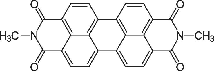
Chemical structure of the Perylene-diimide derivative: N,N′-Dimethyl-3,4,9,10-Perylenetetracarboxylic diimide (DiMe-PTCDI).
The photocurrent (PC) spectra were measured with a Bruker IFS66 FTIR spectrometer operated in fast-scan mode, equipped with a tungsten lamp and a quartz beamsplitter. The samples were illuminated through the silicon substrate by the light beam exiting the Michelson interferometer of the spectrometer. A Si filter in combination with a low-pass interference filter (cut-off at 0.95 eV) and an optional Ge filter were placed in the light beam path. The short-circuit photocurrent of the sample generated by this spectrally-limited beam was amplified by an I–V stage and fed back into the spectrometer electronics via the external detector input.
The noise spectrum was measured with a low noise FEMTO DHPCA-100 I–V stage and a oscilloscope with readout to a PC for the FFT analysis.
For the pulsed and steady-state photocurrent measurements a laser-diode emitting at 1.55 μm was used. Light intensity of the laser-diode was measured with a commercial calibrated InGaAs photodiode placed in the position of the investigated sample. The exact position in the plane perpendicular to the beam for both reference diode and investigated sample, was determined using a X–Y translational stage by optimizing the measured photocurrent for each case. The area of the focused light spot (diameter ≈1.7 mm), visualized by infrared indicating card, was smaller than both the reference diode area (0.03 cm2) and the sample electrode area (0.08 cm2). Therefore it was not necessary to know the exact area of the focused spot, in order to estimate the responsivity of the device under investigation. The light intensity was approximately 200 mW cm−2. The I–V characteristics were measured with a Keithley 236 source meter.
3. Results and discussion
Perylene chromophors are widely used industrially for paints, textiles, and cosmetics. They are characterized by their thermal, excellent chemical, and photochemical stability.
The molecule DiMe-PTCDA is made by derivatizing electron-rich perylene with two mutually-conjugated electron-withdrawing imide groups, resulting in a material with high electron affinity [17]. It is widely believed [18,19] that electron withdrawing imide groups are lowering the electron density as well as lowering the energetic levels of the electron-conducting π∗ molecular orbitals (lowest unoccupied molecular orbital – LUMO) in the inner ring π-system. In contrast to the unsubstituted perylene molecule [20], Perylene diimides are considered as a electron conducting materials, and have been successfully used in organic solar cells [21–23] as well as in thin-film transistors with n-type mobilities on the order of 1 cm2/Vs [24,19,25].
The scanning electron microscope image in Fig. 1 shows the formation of a closed layer of DiMe-PTCDI on top of the p-Si substrate. From the topography of the DiMe-PTCDI surface, it appears that crystallites with lateral dimensions of several hundred nanometers are formed. Such a formation of a closed layer followed by crystallites is a growth mode which typically arises, if the interaction of the molecules with the substrate (e.g. within the first few monolayers of growth) is dominant in comparison to the intermolecular attraction. With increasing layer thickness the growth is not anymore dominantly influenced by Si surface, and the intermolecular attraction between the DiMe-PTCDI molecules leads to the formation of crystallites [26].
In Fig. 3, the current density versus voltage (JV) characteristics of an Al (annealed)/p-Si/DiMe-PTCDI/Al device is presented for measurements at room temperature and at 77 K. At 300 K a current rectification ratio of ≈2 × 10⁴ for a bias variation from −1 to +1 V is observed. Upon cooling, the reverse current density in dark at −1 V bias, decreases from 24 μA cm−2 at 300 K to the pA cm−2 region at 77 K with an increasing current rectification up to ≈3 × 10¹⁰ for a bias variation from −1 to +1 V.
Fig. 3.

Current density–Voltage characteristics (J–V) of the Al/p-Si/DiMe-PTCDI/Al heterojunction photodiode in dark and under IR illumination. (a) at 300 K and illumination with a laser diode emitting at 1.55 μm (in red). The inset shows the J/V characteristics with a logarithmic scale for the current density. (b) illumination by a tungsten lamp spectrally restricted with a combination of a Si and a 0.95 eV low-pass interference filter at 300 K (in red), at 77 K (in green) and with an additional Ge filter at 77 K (in blue) respectively. (For interpretation of the references to color in this figure legend, the reader is referred to the web version of this article.)
Under IR illumination by a spectrally-restricted tungsten lamp (hν < 0.95 eV) and a laser diode emitting at 1.55 μm respectively, a photovoltaic effect is observed. The open circuit voltage is in the mV range at 300 K and increases to ≈0.4 V at 77 K (red and green graph in Fig. 3b). The short circuit current density is weakly temperature-dependent and increased by 37% percent upon cooling from 300 to 77 K. A photovoltaic effect is also observed if a Germanium filter is inserted into the light beam (blue graph in Fig. 3b). Under IR illumination an enhanced current density at forward bias (see inset Fig. 3a) is observed.
Fig. 4 shows the spectrally-resolved photocurrent (PC) at 300 K. The PC spectra are normalized to a responsivity in A/W by measuring the PC upon illumination with a calibrated IR laser diode emitting at 1.55 μm. Above a threshold photon energy of ≈0.5 eV, the PC monotonically increases up to the cut-off of the low-pass interference filter at 0.95 eV. The inset of Fig. 4 shows the spectrally resolved PC at 300 K measured by using an additional Germanium filter in the excitation beam. Typical values of the responsivity at 1.55 μm at 0 and 1 V reverse bias are 0.1 − 0.3 and 2 − 5 mA/W respectively. The value at 0 V bias corresponds to external quantum efficiency (EQE) of ≈9 × 10⁻⁵. A spread in the responsivity is given, due to the fact that the calibration, performed as described at the end of Section 2, was very sensitive to the actual position of the sample in the optical path. To further characterize this architecture as a potential candidate for practical IR-detecting applications, the specific detectivity D∗ is calculated. D∗ is an efficient figure of merit and is defined by the reciprocal of the noise equivalent power per bandwidth (NEP) normalized to the detector sensitive area A, and is given by:
| (1) |
where . R is the responsivity and is the mean square of the thermal noise current per bandwidth Δf. In Fig. 5 the spectral noise current density at 0 V bias of the p-Si/DiMe-PTCDI photodiode at 300 K is plotted (red trace) together with the one of a 10 kΩ resistor (green trace). The mean square of the noise current density of a resistor r is given by [27] and agrees with the measured data and hence supports the realistic value of D∗. At low frequencies an 1/f noise is observed followed by a nearly flat (white) region up to the roll-off (f > 100 kHz) of the I–V stage. The capacitance of the photodiode causes the slight decrease of the low roll-off frequency of the I–V stage compared to the pure resistive load. In the white noise region we find a D∗ value of ≈7 × 10⁷ Jones. The time-resolved IR photocurrent at 0 V bias is shown in Fig. 6. Similar rise and fall times in the range of 300 ns are observed. Due to the large active area, the time response is most likely limited by the RC time constant rather than by the intrinsic properties of the heterojunction [28]. In Fig. 7 is shown the capacitance–voltage (1/C(V)2) characteristics. For reverse bias (p-Si negative with respect to the organic thin film) the square of the inverse capacitance depends linearly on the applied bias. Such a behavior is characteristic for the formation of a depletion zone in the p-Si. As slight hysteresis around zero bias is observed for a continuous increasing (forward) and reducing (backward) bias potentials. The hysteresis is vanishing when applying a stepwise change (delay of 0.3 s after each step) of the bias potentials. The hysteresis is presumably caused by trapped charges in the DiMe-PTCDI. The slope of a linear interpolation (red line in Fig. 7) is inversely proportional to the boron doping concentration NA in the p-Si [29]
| (2) |
In agreement with the wafer specifications the doping concentration reads as NA = 2 × 1015 cm−3. Eq. (2) neglects interfacial trap states, minority charge but is applicable to deep depletion [29]. The classic evaluation of the build-in potential via linear extrapolation (in Fig. 7 from the intercept of the linear interpolation with the abscissa) does in the present case lead to erroneous results as the organic thin film introduces a capacitance and a voltage drop [30]. Another difference compared with a pure Schottky contact is the low reverse dark current density of the heterojunction. In the supplementary material it is outlined that the reverse dark current density is several orders of magnitude smaller than predicted by thermionic emission theory for Schottky diodes. Consequently the thermionic emission theory is hardly feasible (i.e. needs to be extended [31]) to account for the low reverse dark current density.
Fig. 4.

Spectrally resolved photocurrent at 300 K. Illumination by the same spectrally restricted tungsten lamp (hν < 0.95 eV) as used for the measurements in Fig. 3b. The inset shows the spectrally resolved photocurrent using a Ge filter.
Fig. 5.

Double logarithmic presentation of the spectral noise density versus frequency at 0 V bias and 300 K of the Al/p-Si/DiMe-PTCDI/Al photodiode (red), and of a 10 kΩ metal-film resistor (green). (For interpretation of the references to color in this figure legend, the reader is referred to the web version of this article.)
Fig. 6.

Time-resolved photocurrent at 0 V bias and 300 K upon excitation by a pulsed laser diode emitting at 1.55 μm.
Fig. 7.

1/C2 versus applied bias of the Al/p-Si/DiMe-PTCDI/Al heterojunction photodiode. The modulation frequency is 1 kHz and the AC amplitude is 5 mV.
The observed photoresponse as well as the rectifying JV characteristics of the p-Si/DiMe-PTCDI heterojunction can be understood in terms of the electron and hole band discontinuities across the interface that are sketched schematically in Fig. 8. The band-diagram has similarities to a metal/insulator/semiconductor (MIS) structure. By assuming that the pictured barrier height is associated with the onset of PC, the electron conducting extended electronic states (i.e. LUMO and the higher unoccupied states) of the organic thin film are energetically within the bandgap of the p-Si [32]. At forward bias (p-Si positive relative to the DiMe-PTCDI) electrons are efficiently injected from the Al top-contact into the DiMe-PTCDI layer. The electron injection from the DiMe-PTCDI into the Si conduction band (CB) is energetically unfavorable and the current has to traverse the inorganic/organic interface as a recombination current between electrons in the DiMe-PTCDI and holes in the p-Si. When biasing the p-Si/DiMe-PTCDI diode in reverse direction (negative voltage applied to the Al/p-Si back contact), holes are extracted from the p-Si valence band (VB) into the Al back-contact [1].
Fig. 8.

Energy-band diagram for the Al/p-Si/DiMe-PTCDI/Al heterojunction photodiode at zero bias.
Similar to our previous work [1], we ascribe the photovoltaic behavior of the p/Si DiMe/PTCDI junction to an effective excitation of an electron from the Si valence band into the extended LUMO state in the DiMe-PTCDI. Whether this excitation occurs as spatially indirect transition or rather via an intermediate, occupied localized DiMe-PTCDI surface state (as indicated by the vertical arrow in Fig. 8) cannot be decided. However, a similar process for sub-bandgap photoresponse for organic modified GaAs Schottky diodes via an intermediate occupied localized state is proposed by Hsu et al. [33] and is extensively reviewed in Ref. [34] (referred therein as a pseudo internal photoemission process). The increase of performance as compared to p-Si/PCBM diode is tentatively ascribed to more efficient photoexcitation of electrons due to a larger density of localized states with long life-times, that might also be the reason for the hysteresis in C–V experiment.
In addition, under forward bias a photoconductive effect is observed (see inset of Fig. 3a), which we ascribe to an increase of the free electron concentration in the DiMe-PTCDI film by optically exciting electrons trapped in localized DiMe-PTCDI bulk states.
4. Conclusion
In summary it is demonstrated that an organic/inorganic heterojunction can be utilized for sensing NIR light (specifically at 1.55 μm). A photovoltaic effect up to 2.7 μm is observed and it is argued that it originates from an optical excitation of occupied localized states in the organic thin film with a subsequent charge-carrier separation at the heterointerface. The simple fabrication, operation at room-temperature, compatibility with the CMOS process together with the responsivity, specific detectivity and response time reported here demonstrate the potential of this device concept.
Thirty years ago, Forrest et al. demonstrated organic–inorganic heterojunction devices [35]. In his review from 2003 [36] Forrest asked for an application niche for such a device concept where its advantages over conventional or even all-organic devices, such as low environmental and energetic cost of fabrication and integration with Si ICs, room temperature operation and low power consumption (short circuit operation), would be shown. The use of such a structure for IR detection could indeed be one.
In order to increase the performance of the device further experiments are planned, aiming at better understanding of the photoexcitation process (for example photo induced absorption) and probing of localized states with transient electrical methods.
Acknowledgements
This work was supported by the Österreichische Forschungsförderungsgesellschaft (FFG project number 818046). The authors thank Prof. G. Bauer for valuable discussions.
Footnotes
Supplementary data associated with this article can be found, in the online version, at http://dx.doi.org/10.1016/j.orgel.2013.02.009.
Appendix A. Supplementary material
References
- 1.Matt Gebhard J., Fromherz Thomas, Bednorz Mateusz, Zamiri Saeid, Goncalves Guillaume, Lungenschmied Christoph, Meissner Dieter, Sitter Helmut, Sariciftci Niyazi Serdar, Brabec Christoph J., Bauer Günther. Fullerene sensitized silicon for near- to mid-infrared light detection. Advanced Materials (Deerfield Beach, Fla.) 2010;22(5):647–650. doi: 10.1002/adma.200901383. < http://onlinelibrary.wiley.com/doi/10.1002/adma.200901383/abstract>. [DOI] [PubMed] [Google Scholar]
- 2.Our choice from the recent literature, Nature Photonics 4(3) (2010) 128–129, doi: 10.1038/nphoton.2010.9. <http://www.nature.com/doifinder/10.1038/nphoton.2010.9>.
- 3.Muramoto Y., Ishibashi T. InPInGaAs pin photodiode structure maximising bandwidth and efficiency. Electronics Letters. 2003;39(24):1749. doi: 10.1049/el:20031116. < http://digital-library.theiet.org/content/journals/10.1049/el_20031116>. [Google Scholar]
- 4.Casalino M., Sirleto L., Iodice M., Saffioti N., Gioffre M., Rendina I., Coppola G. Cu/p-Si Schottky barrier-based near infrared photodetector integrated with a silicon-on-insulator waveguide. Applied Physics Letters. 2010;96(24):241112. < http://link.aip.org/link/APPLAB/v96/i24/p241112/s1&Agg=doi>. [Google Scholar]
- 5.Knights A., House A., MacNaughton R., Hopper F. Optical power monitoring function compatible with single chip integration on silicon-on-insulator. Conference on Optical Fiber Communication. 2003;2:705–706. [Google Scholar]
- 6.Liu Y., Chow C.W., Cheung W.Y., Tsang H.K. In-line channel power monitor based on helium ion implantation in silicon-on-insulator waveguides. IEEE Photonics Technology Letters. 2006;18(17):1882–1884. [Google Scholar]
- 7.Baehr-Jones T., Hochberg M., Scherer A. Photodetection in silicon beyond the band edge with surface states. Optics Express. 2008;16(3):1659–1668. doi: 10.1364/oe.16.001659. < http://www.ncbi.nlm.nih.gov/pubmed/18542245>. [DOI] [PubMed] [Google Scholar]
- 8.Zhu Shiyang, Yu M.B., Lo G.Q., Kwong D.L. Near-infrared waveguide-based nickel silicide Schottky-barrier photodetector for optical communications. Applied Physics Letters. 2008;92(8):81103. < http://link.aip.org/link/?APL/92/081103/1>. [Google Scholar]
- 9.Tanabe Takasumi, Sumikura Hisashi, Taniyama Hideaki, Shinya Akihiko, Notomi Masaya. All-silicon sub-Gb/s telecom detector with low dark current and high quantum efficiency on chip. Applied Physics Letters. 2010;96(10):101103. < http://link.aip.org/link/?APL/96/101103/1>. [Google Scholar]
- 10.Baierl Daniela, Pancheri Lucio, Schmidt Morten, Stoppa David, Betta Gian-Franco Dalla, Scarpa Giuseppe, Lugli Paolo. A hybrid CMOS-imager with a solution-processable polymer as photoactive layer. Nature Communications. 2012;3:1175. doi: 10.1038/ncomms2180. <http://dx.doi.org/10.1038/ncomms2180 http://www.nature.com/ncomms/journal/v3/n10/suppinfo/ncomms2180_S1. html>. [DOI] [PubMed] [Google Scholar]
- 11.Kern W., Puotinen D.A. Cleaning solutions based on hydrogen peroxide for use in silicon semiconductor technology. RCA Review. 1970;31(2):187–206. [Google Scholar]
- 12.Herman Marian A., Sitter Helmut. Springer Series in Materials Science. second ed. Springer-Verlag; Berlin, Heidelberg, New York: 1996. Molecular beam epitaxy – fundamentals and current status. [Google Scholar]
- 13.Lopez-Otero A. Hot wall epitaxy. Thin Solid Films. 1978;49(1):3–57. < http://linkinghub.elsevier.com/retrieve/pii/0040609078903097>. [Google Scholar]
- 14.Sitter Helmut, Andreev Andrei Yu, Matt Gebhard J., Sariciftci Niyazi Serdar. Hot-wall-epitaxy – the method of choice for the growth of highly ordered organic epilayers. Molecular Crystals and Liquid Crystals. 2002;385:51–60. < http://www.tandfonline.com/doi/abs/10.1080/713738791>. [Google Scholar]
- 15.Gebhard J. Matt, Fullerene-oligopheny multilayers grown by Hot Wall Epitaxy. Master Thesis Johannes Kepler University.
- 16.Andreev Andrei Yu, Matt Gebhard J., Brabec Christoph J., Sitter Helmut, Badt D., Seyringer H., Sariciftci N.S. Highly anisotropically self-assembled structures of para-sexiphenyl grown by hot-wall epitaxy. Advanced Materials. 2000;12(9):629–633. <http://doi.wiley.com/10.1002/(SICI)1521-4095(200005)12:9<629::AID- ADMA629>3.3.CO;2-J, doi:10.1002/(SICI)1521-4095(200005)12:9<629::AID-ADMA629>3.3.CO;2-J>. [Google Scholar]
- 17.Anthony John E., Facchetti Antonio, Heeney Martin, Marder Seth R, Zhan Xiaowei. n-Type organic semiconductors in organic electronics. Advanced Materials (Deerfield Beach, Fla.) 2010;22(34):3876–3892. doi: 10.1002/adma.200903628. <http://onlinelibrary.wiley.com/doi/10.1002/adma.200903628/abstract, doi:10.1002/adma.200903628>. [DOI] [PubMed] [Google Scholar]
- 18.Meyer J. Charge transport in thin films of molecular semiconductors as investigated by measurements of thermoelectric power and electrical conductivity. Thin Solid Films. 1995;258(1–2):317–324. <http://linkinghub.elsevier.com/retrieve/pii/0040609094063699>. [Google Scholar]
- 19.Jones Brooks A., Ahrens Michael J., Yoon Myung-Han, Facchetti Antonio, Marks Tobin J., Wasielewski Michael R. High-mobility air-stable n-type semiconductors with processing versatility: dicyanoperylene-3,4:9,10-bis(dicarboximides) Angewandte Chemie (International ed. in English) 2004;43(46):6363–6366. doi: 10.1002/anie.200461324. <http://onlinelibrary.wiley.com/doi/10.1002/anie.200461324/abstract, doi:10.1002/anie.200461324>. [DOI] [PubMed] [Google Scholar]
- 20.Lee Jin-Woo, Kang Han-Saem, Kim Min-Ki, Kim Kihyun, Cho Mi-Yeon, Kwon Young-Wan, Joo Jinsoo, Kim Jae-Il, Hong Chang-Seop. Electrical characteristics of organic perylene single-crystal-based field-effect transistors. Journal of Applied Physics. 2007;102(12):124104. <http://link.aip.org/link/JAPIAU/v102/i12/p124104/s1& Agg=doi>. [Google Scholar]
- 21.Tang Ching W. Two-layer organic photovoltaic cell. Applied Physics Letters. 1986;48(2):183. <http://link.aip.org/link/APPLAB/v48/i2/p183/s1& Agg=doi>. [Google Scholar]
- 22.Rostalski Jörn. Photocurrent spectroscopy for the investigation of charge carrier generation and transport mechanisms in organic p/n-junction solar cells. Solar Energy Materials and Solar Cells. 2000;63(1):37–47. <http://linkinghub.elsevier.com/retrieve/pii/S0927024800000180>. [Google Scholar]
- 23.Ferrere Suzanne, Gregg Brian A. New perylenes for dye sensitization of TiO2. New Journal of Chemistry. 2002;26(9):1155–1160. < http://pubs.rsc.org/en/Content/ArticleLanding/2002/NJ/b203260k>. [Google Scholar]
- 24.Malenfant Patrick R.L., Dimitrakopoulos Christos D., Gelorme Jeffrey D., Kosbar Laura L., Graham Teresita O., Curioni Alessandro, Andreoni Wanda. N-type organic thin-film transistor with high field-effect mobility based on a N,N[sup]-dialkyl-3,4,9,10-perylene tetracarboxylic diimide derivative. Applied Physics Letters. 2002;80(14):2517. <http://link.aip.org/link/APPLAB/v80/i14/p2517/s1& Agg=doi>. [Google Scholar]
- 25.Chesterfield Reid J., McKeen John C., Newman Christopher R., Ewbank Paul C., Filho Demétrio A da Silva, Brédas Jean-Luc, Miller Larry L., Mann Kent R., Frisbie C. Daniel. Organic thin film transistors based on N-Alkyl perylene diimides: charge transport kinetics as a function of gate voltage and temperature. The Journal of Physical Chemistry B. 2004;108(50):19281–19292. < http://pubs.acs.org/doi/abs/10.1021/jp046246y>. [Google Scholar]
- 26.Gustafsson J.B., Moons E., Widstrand S.M., Johansson L.S.O. Thin PTCDA films on Si(001): 1. growth mode. Surface Science. 2004;572(1):23–31. < http://linkinghub.elsevier.com/retrieve/pii/S0039602804010751>. [Google Scholar]
- 27.Nyquist H. Thermal agitation of electric charge in conductors. Physical Review. 1928;32(1):110–113. <http://link.aps.org/doi/10.1103/PhysRev.32.110>. [Google Scholar]
- 28.Ginev G., Riedl T., Parashkov R., Johannes H.-H., Kowalsky W. Organic-GaAs heterostructure diodes for microwave applications. Applied Surface Science. 2004;234(1–4):22–27. < http://linkinghub.elsevier.com/retrieve/pii/S0169433204007299>. [Google Scholar]
- 29.Schroder Dieter K. third ed. John Wiley & Sons, Inc.; 2006. Semiconductor Material and Device Characterization. [Google Scholar]
- 30.Forrest Stephen R., Kaplan M.L., Schmidt P.H. Organic-on-inorganic semiconductor contact barrier diodes. I. Theory with applications to organic thin films and prototype devices. Journal of Applied Physics. 1984;55(6):1492. <http://link.aip.org/link/JAPIAU/v55/i6/p1492/s1& Agg=doi>. [Google Scholar]
- 31.Antohe S., Tomozeiu N., Gogonea S. Properties of the organic-on-inorganic semiconductor barrier contact diodes In/PTCDI/p-Si and Ag/CuPc/p-Si. Physica Status Solidi (a) 1991;125(1):397–408. <http://doi.wiley.com/10.1002/pssa.2211250138>. [Google Scholar]
- 32.Zahn Dietrich R.T., Kampen Thorsten U., Méndez Henry. Transport gap of organic semiconductors in organic modified Schottky contacts. Applied Surface Science. 2003;212–213:423–427. <http://linkinghub.elsevier.com/retrieve/pii/S0169433203001259>. [Google Scholar]
- 33.Hsu Julia W.P., Lang David V., West Kenneth W., Loo Yueh-Lin, Halls Mathew D., Raghavachari Krishnan. Probing occupied states of the molecular layer in Au-alkanedithiol-GaAs diodes. The Journal of Physical Chemistry B. 2005;109(12):5719–5723. doi: 10.1021/jp044246s. <http://pubs.acs.org/doi/abs/10.1021/jp044246s>. [DOI] [PubMed] [Google Scholar]
- 34.Afanas’ev V.V. Elsevier Science; 2008. Internal Photoemission Spectroscopy: Principles and Applications. [Google Scholar]
- 35.Forrest Stephen R. Organic-on-inorganic semiconductor contact barrier devices. Applied Physics Letters. 1982;41(1):90. <http://link.aip.org/link/?APL/41/90/1& Agg=doi>. [Google Scholar]
- 36.Forrest Stephen R. Organic-inorganic semiconductor devices and 3,4,9,10 perylenetetracarboxylic dianhydride: an early history of organic electronics. Journal of Physics: Condensed Matter. 2003;15(38):S2599–S2610. <http://iopscience.iop.org/0953-8984/15/38/001/>. [Google Scholar]
Associated Data
This section collects any data citations, data availability statements, or supplementary materials included in this article.