Abstract
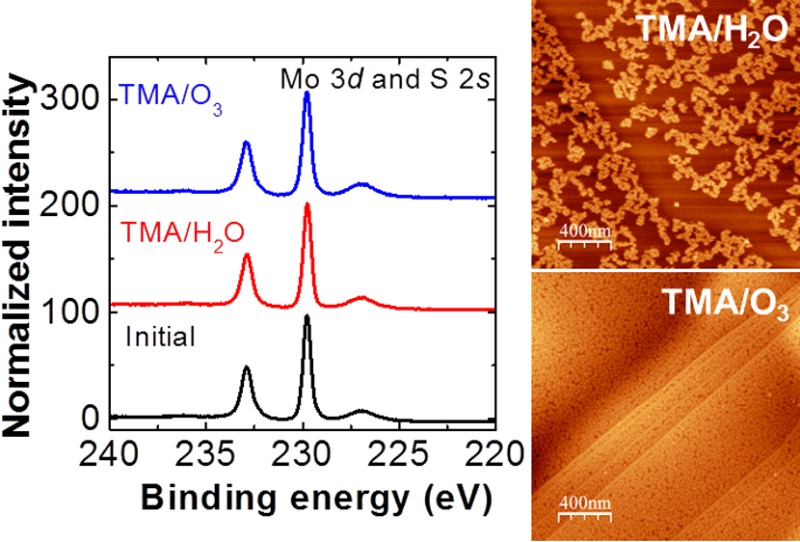
We present an Al2O3 dielectric layer on molybdenum disulfide (MoS2), deposited using atomic layer deposition (ALD) with ozone/trimethylaluminum (TMA) and water/TMA as precursors. The results of atomic force microscopy and low-energy ion scattering spectroscopy show that using TMA and ozone as precursors leads to the formation of uniform Al2O3 layers, in contrast to the incomplete coverage we observe when using TMA/H2O as precursors. Our Raman and X-ray photoelectron spectroscopy measurements indicate minimal variations in the MoS2 structure after ozone treatment at 200 °C, suggesting its excellent chemical resistance to ozone.
Keywords: atomic layer deposition, high-k dielectric, ozone, MoS2
Molybdenum disulfide (MoS2) is a promising 2D semiconductor, with a layered structure similar to graphene and an intrinsic band gap,1 that exhibits interesting electronic properties such as high field mobility (up to ∼500 cm2 V–1 s–1), low subthreshold swing (∼70 mV/dec), and high current on/off ratio (∼1 × 10⁸).2−4 To fabricate high-performance devices based on MoS2, high-k dielectrics such as HfO23,5or Al2O32,4,6 with thicknesses of 10–30 nm have been used as top-gate insulators because they improve the field-effect electron mobility of the channel by reducing Coulombic scattering.7 In these studies, the dielectric layers were deposited by atomic layer deposition (ALD) because of its unparalleled conformality and uniformity as well as its ability to control film thickness on the atomic level. However, it is difficult to deposit high-quality high-k dielectrics onto the surfaces of 2D semiconductors such as graphene8 and MoS29,10 because of the chemical inertness of their basal planes. Recently, Liu et al. reported that depositing uniform Al2O3 (∼10 nm thickness) on MoS2 could only be achieved at substrate temperatures below 200 °C via a physical adsorption mechanism.2,9 However, physical adsorption of the precursors causes the film coverage to depend on growth parameters such as pulsing and purging times, process pressure, and cleanliness of the MoS2 surface. For example, Yang et al.11 could not produce uniform ALD-Al2O3 on MoS2 after depositing the same number of cycles used by Liu et al. In addition, the use of low-temperature ALD raises concerns regarding high levels of impurities, such as OH and C residues,12 in the dielectric film. To overcome these limitations and grow a uniform dielectric layer, Yang et al.11 functionalized the MoS2 surface with oxygen plasma prior to ALD at 250 °C. However, they observed significant interfacial oxidation, indicated by the emergence of the Mo6+ chemical state, and lattice disordering induced by physical plasma damage. Additionally, both Liu et al. and Yang et al. needed to deposit up to 10 nm of dielectric to produce uniform films, which is undesirable considering the constant downscaling to physical thicknesses less than 3 nm required by the microelectronics industry.
Recently, Azcatl et al.13 reported the growth of uniform Al2O3 films on room temperature UV-ozone functionalized MoS2 surface using TMA/H2O-ALD at 200 °C due to the formation of weak S–O bonds, and suggested UV exposure is essential for this oxygen adsorption at low pressure because of the increased reactivity of radical O· generated by UV light. However, long time UV exposure could affect the optical and electrical properties of MoS2.14 Previous study shows that UV light exposure could induce photochemical reactivity degradation on graphene surfaces.15 In addition, it is reported that room-temperature TMA/ozone treatment on graphene results in highly scalable high-k deposition with excellent conformality.16
In this letter, we carefully investigated how ozone-based ALD affected the MoS2 interface. Our experimental results suggest that ozone-based ALD can be used to fabricate smooth, uniform Al2O3 layers with thicknesses of 5 nm or less without noticeable oxidization of the MoS2 interface. Ozone, compared with H2O and oxygen plasma as oxidant precursors, has well-recognized advantages, such as higher reactivity,17relatively easy purging, and good compatibility with batch processes, in addition to producing lower defect-state density, lower leakage current, and fewer OH and related defect states12,17in the resulting ALD films. The present letter studies the reaction behavior of ozone with the MoS2 surface and the feasibility of depositing high-k dielectrics using ozone-based ALD.
Figure 1a shows a representative AFM topographic image of an ALD-Al2O3 layer deposited on a MoS2 flake with 30 cycles of TMA/H2O at 200 °C. The thickness of the Al2O3 layer is ∼3.0 nm with a vertical growth rate of ∼1.0 Å/cycle, determined by the corresponding AFM line profile. In contrast to the uniform Al2O3 layer deposited at 200 °C by Liu et al.,2 the Al2O3 layer reported in the present letter exhibits less than 40% coverage, revealed by the formation of dispersed Al2O3 clusters resembling the Al2O3-ALD film on a MoS2 surface, as reported by Yang11 and Azcatl13 et al. When using TMA/H2O, we observed more rapid Al2O3 growth along the step edge of the MoS2 flake than on the terraces, indicated by the AFM line profile (∼1.2 nm step height). This behavior was likely caused by the presence of dangling bonds at the edge, which commonly react more readily during initial ALD nucleation.18 We obtained a uniform Al2O3 layer (RMS roughness of ∼1.2 nm) by replacing water with ozone as the oxidizing agent, as shown in Figure 1b. An AFM line profile confirms the film thickness to be ∼3.1 nm, grown at a rate of ∼1.0 Å/cycle, which agrees well with a previously reported growth rate on highly oriented pyrolytic graphite (HOPG).18 With the same precursor purge and pulse times as the TMA/H2O-ALD process, using ozone enhances the Al2O3 film coverage and uniformity on both the MoS2 step edges and basal planes, suggesting that the ozone facilitates initial TMA precursor nucleation on the MoS2 by increasing the number of activation sites.19 It is believed that the differing growth behavior at 200 °C when using TMA/O3 is associated with the distinct interaction mechanisms of ozone with the MoS2 surface. Different than water, ozone readily decomposes into molecular O2 and monatomic O upon reaching the surface; the latter is considered to be the active species providing TMA nucleation sites through weak surface adsorption.13,17,19 At higher temperatures, the complicated concomitance of O radical diffusion and desorption tends to govern the growth of the Al2O3 film, leading to higher surface roughness.17,19
Figure 1.
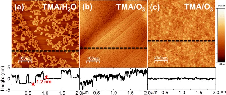
AFM images of the ALD-Al2O3 layer deposited using (a) TMA/H2O at 200 °C (30 cycles), (b) TMA/O3 (30 cycles) at 200 °C, and (c) TMA/O3 (5 cycles of seeding layer at 30 °C, followed by 45 cycles of ALD at 200 °C).
In an attempt to deposit a uniform, thin Al2O3 layer on MoS2, we deposited five cycles of TMA/O3 at 30 °C as a seeding layer prior to sequential ALD at 200 °C. Figure 1c shows an AFM image of the conformal Al2O3 layer after 45 cycles of TMA/O3 at 200 °C. The thickness of this oxide layer is ∼5.1 nm, determined by using an ellipsometer (Sentech 800) against a reference measurement of an Al2O3 layer grown on H-terminated Si. In contrast to the film shown in Figure 1b, this Al2O3 film grown on the seeding layer has a fairly smooth surface (RMS roughness of ∼0.23 nm vs RMS roughness of ∼0.18 nm for clean MoS2. Our results indicate that a thin (∼5 nm or less) and uniform dielectric layer can be deposited by first depositing a thin seeding layer (∼1 nm) before performing TMA/O3-ALD at a higher temperature. Similar to ozone-based ALD on graphene,20 it is suggested that using a seeding layer also prevents the formation of possible ozone-etch-related defects induced by high-temperature interactions between the ozone and surface.
LEIS microscopy is an extremely surface-sensitive technique capable of detecting chemical species in the topmost layer of deposited films.21 In Figure 2, ex situ LEIS spectra of the surface elemental compositions show only O (404 eV) and Al (573 eV) peaks, originating from the Al2O3 layer, for the samples prepared using ALD with TMA/ozone precursors The absence of S (625 eV) and Mo (838 eV) signals, regardless of substrate temperature, from the underlying MoS2 substrate indicates that 30 cycles of ALD produced full-coverage films. In contrast, we detected four peaks assigned to O, Al, S, and Mo on the surface after 50 cycles of TMA/H2O-ALD, clear evidence of incomplete film coverage. Because the Mo scattering cross-section is four times larger than that of S atoms,21 the peak ratio of S and Mo atoms suggests that more S than Mo is present in the first layer, in agreement with the stoichiometry of MoS2. These LEIS results, which complement our AFM images, suggest that ozone-based ALD more effectively deposits uniform dielectric layers on MoS2.
Figure 2.
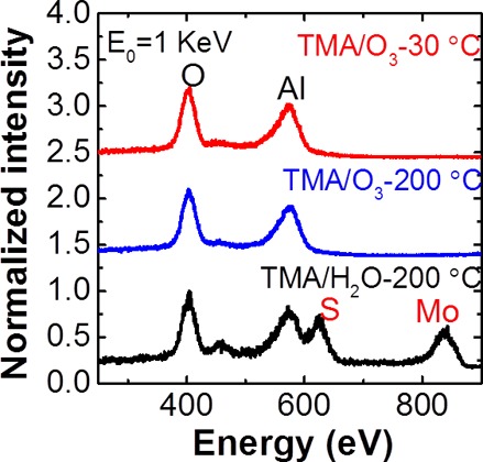
LEIS spectra of the topmost layers of ALD-Al2O3 films deposited using TMA/O3 (30 cycles) at 30 and 200 °C as well as TMA/H2O (50 cycles) at 200 °C.
Figure 3a, b show the ex situ Raman spectra of a monolayer-thick MoS2 flake exposed to ozone at 30 or 200 °C for 10 s; we assessed the thickness of the flake by interpreting the ∼18.2 cm–1 separation between the two peaks present. Raman spectroscopy has been widely used to study the 2D crystalline structure of MoS2 because of its ability to detect its characteristic phonon modes.21 The prominent peak observed at low Raman shifts of around ∼384 cm–1 is attributed to S–Mo–S in-plane motion (E2g1 mode), whereas the peak at ∼402 cm–1 is assigned to out-of plane motion (A1g mode).22 These two Raman active modes have been reported to shift with changes in thickness,23 strain,24 temperature,25 and doping;26 therefore, they are considered a signature of the stoichiometric MoS2 lattice structure. Figure 3a shows that exposing MoS2 to ozone at 30 °C for 10 s (∼380 g/Nm3, P[O3]= ∼150 Torr) does not observably alter its Raman signals compared with its as-exfoliated peaks. At 200 °C for 10 s, the S–Mo–S out-of-plane A1g mode at ∼402 cm–1 shifts down by ∼0.6 cm–1 and broadens by ∼0.3 cm–1. We recorded Raman spectra from up to five positions on each sample to ensure that this peak shift was not caused by measurement errors; additionally, our Renishaw Raman spectroscopy instrument can detect Raman frequency shifts as low as 0.1 cm–1. This finding agrees with an in situ Raman study performed on top-gated single-layer MoS2 transistors,26 in which electron doping caused the A1g mode to red-shift and broaden, but did not affect the E2g peak. In the present letter, the absence of noticeable alterations to the MoS2 Raman active modes and the lack of the MoO327 Raman frequency at ∼820 cm–1 suggests that exposing the MoS2 to ozone did not significantly disorder its lattice. Reports have shown that MoS2 is relatively stable in oxygen-rich environments at temperatures up to 370 °C27 because of its high Mo–S dissociation binding energy (∼368 kJ/mol).28 Therefore, our Raman analysis of monolayer MoS2 suggests that the improved coverage of the Al2O3 film when using TMA/O3 as precursors can be traced to the relatively weak interaction between the oxygen species and MoS2; the sulfur and oxygen interactions that do occur are not strong enough to alter the MoS2 lattice at room temperature, but can supply additional activation sites for initial TMA nucleation. Although, in this case the formation of possible weak S–O bond could not be excluded during ozone exposure, which is beyond the detections of our ex situ Raman studies.
Figure 3.
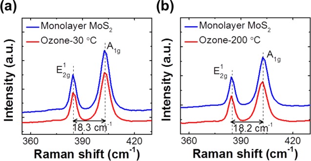
Raman spectra of as-exfoliated monolayer MoS2 (top) after O3 treatment (bottom) at (a) 30 °C for 10 s and (b) 200 °C for 10 s.
To consolidate the evidence of the chemical stability of MoS2 against ozone etching, which can degrade device characteristics,20 we used ex situ XPS to examine the binding energies of Mo 3d, S 2s, and S 2p core states for MoS2 after 30 ALD cycles at 200 °C using TMA/O3 or TMA/H2O, and compared them with those of an as-exfoliated MoS2 crystal. Shown in Figure 4a, b, we assign the binding energies at ∼232.96 and ∼229.83 eV to the Mo 3d3/2 and Mo 2d5/2 chemical states, whereas we assign the peaks at ∼227.05 and ∼162.7 eV to the S 2s and S 2p core levels, which originate from the corresponding Mo(IV) and S(II) chemical states in the MoS2 crystal.11 For both samples, depositing Al2O3 on MoS2 significantly decreases the intensities of the Mo and S peaks because of XPS signal attenuation; we also observed similar peak-intensity attenuation in the S 2p region at ∼162.7 eV. The good overlap of the Mo 3d and S 2p peaks over those of as-exfoliated MoS2 suggest no detectable Mo oxidation or S substitution with O in the S–Mo–S lattice; the detection limit of XPS system used in this work is about 1%; these XPS results support the fact that MoS2 demonstrates better chemical stability against ozone treatment compared with that of graphene, in which ozone exposure at 200 °C leads to graphene surface damage arising from ozone etches,19,20 but no apparent evidence of MoS2 interface structure changes is seen in our Raman and XPS investigations. Compared to pretreating MoS2 with oxygen plasma,11 using ozone could be a less damaging way of depositing dielectric films.
Figure 4.
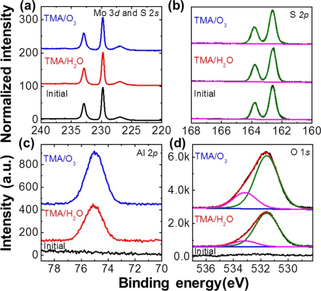
XPS spectra of MoS2 samples after ALD at 200 °C with TMA/O3 or TMA/H2O precursors, deposited with reference to an initial MoS2 crystal. (a) Mo 3d and S 2s, (b) S 2p, (c) Al 2p, and (d) O 1s core levels.
Figure 4c, d shows the XPS binding energies of Al 2p and O 1s in the Al2O3 layers deposited by ALD at 200 °C with TMA/O3 and TMA/H2O precursors, respectively. For both samples, the Al 2p peaks are composed of a predominant chemical state centered at ∼74.9 eV; we measured the binding energy difference between Al–O to be ∼456.6 eV, which agrees well with the previously reported binding energies of Al 2p for O–Al–O in fully oxidized Al2O3 films.29 The peak intensity of the Al 2p state in the TMA/O3 film is ∼50% greater than that of the TMA/H2O film, consistent with the average film thicknesses of ∼1.9 nm (TMA/O3) and ∼1.1 nm (TMA/H2O) derived from attenuations of the Mo 3d core-level peak intensity. Note that the average film thicknesses calculated from XPS measurements are considered to be underestimated because of two reasons: Mo signal intensity could be enhanced after ozone exposure which is found to remove carbon residues (∼50%) adsorbed from environment after MoS2 exfoliation; the average film thickness in XPS is derived over a relatively large area, while the AFM line profiles show only the relative film thickness with respect to the underlying layer. Figure 4d shows the O 1s core levels for both samples, deconvoluted into two main components. The lower binding energy peak at ∼531.5 eV, close to the O 1s peak of sapphire at ∼531.1 eV,30 is associated with Al–O bonds. The higher binding energy peak at ∼533.1 eV is attributed to multiple intermediate species, including hydroxyl aluminum, carbonyl, formate, and methoxyl, caused by incomplete reactions of the metalorganic precursors.31 The greater peak intensity at ∼533.1 eV for the TMA/O3-ALD film over that of the TMA/H2O-ALD film could have been caused by carbon oxidation by ozone, contributing extra carbon to the film.
In summary, we investigated the growth of high-k dielectric Al2O3 layers on MoS2 using ALD with TMA/H2O and TMA/O3 precursors. Our AFM and LEIS results indicated that using ozone greatly improved the film coverage and deposition rate because of accelerated TMA nucleation. We fabricated a conformal layer of Al2O3 using a thin seeding layer prior to performing high-temperature ozone-based ALD. The absence of noticeable oxidation states from the MoS2 interface after TMA/ozone process at 200 °C suggests that MoS2 is likely more chemically resistant to ozone etches than graphene.
Acknowledgments
The authors thank Mr. G. Mordi and Dr. S. McDonnell for their helpful discussions and thank TMEIC for providing the ozone generator (TMEIC OP-250OH-LT ozone system). This work was partially supported through the SWAN (NIST) program. K.C. and R.M.W. acknowledge financial support from LEAST.
Supporting Information Available
Experimental details for the exfoliation of MoS2 flakes of varied thickness on SiO2/Si surfaces and ALD deposition of Al2O3 films, information on the characterization techniques used for surface analysis. This material is available free of charge via the Internet at http://pubs.acs.org.
The authors declare no competing financial interest.
Funding Statement
National Institutes of Health, United States
Supplementary Material
References
- Mak K. F.; Lee C. G.; Hone J.; Shan J.; Heinz T. F. Atomically Thin MoS2: A New Direct-Gap Semiconductor. Phys. Rev. Lett. 2010, 105, 136805. [DOI] [PubMed] [Google Scholar]
- Liu H.; Neal A. T.; Du Y.; Ye P. D. Fundamentals in MoS2 Transistors: Dielectric, Scaling and Metal Contacts. ECS Trans. 2013, 58, 203–208. [Google Scholar]
- Radisavljevic B.; Radenovic A.; Brivio J.; Giacometti V.; Kis A. Single-layer MoS2 Transistors. Nat. Nanotechnol. 2011, 6, 147–150. [DOI] [PubMed] [Google Scholar]
- Kim S.; Konar A.; Hwang W. S.; Lee J. H.; Lee J.; Yang J.; Jung C.; Kim H.; Yoo J. B.; Choi J. Y.; Jin Y. W.; Lee S. Y.; Jena D.; Choi W.; Kim K. High-mobility and Low-power Thin-film Transistors Based on Multilayer MoS2 Crystals. Nat. Commun. 2012, 3, 1011. [DOI] [PubMed] [Google Scholar]
- Lembke D.; Kis A. Breakdown of High-Performance Monolayer MoS2 Transistors. ACS Nano 2012, 6, 10070–10075. [DOI] [PubMed] [Google Scholar]
- Das S.; Chen H. Y.; Penumatcha A. V.; Appenzeller J. High Performance Multilayer MoS2 Transistors with Scandium Contacts. Nano Lett. 2013, 13, 100–105. [DOI] [PubMed] [Google Scholar]
- Jena D.; Konar A. Enhancement of Carrier Mobility in Semiconductor Nanostructures by Dielectric Engineering. Phys. Rev. Lett. 2007, 98, 136805. [DOI] [PubMed] [Google Scholar]
- Kim J. Y.; Jandhyala S. Atomic Layer Deposition of Dielectrics for Carbon-based Electronics. Thin Solid Films 2013, 546, 85–93. [Google Scholar]
- Liu H.; Xu K.; Zhang X. J.; Ye P. D. The Integration of high-k Dielectric on Two-Dimensional Crystals by Atomic Layer Deposition. Appl. Phys. Lett. 2012, 100, 152115. [Google Scholar]
- McDonnell S.; Brennan B.; Azcatl A.; Lu N.; Dong H.; Buie C.; Kim J. Y.; Hinkle C. L.; Kim M. J.; Wallace R. M. HfO2 on MoS2 by Atomic Layer Deposition: Adsorption Mechanisms and Thickness Scalability. ACS Nano 2013, 7, 10354–10361. [DOI] [PubMed] [Google Scholar]
- Yang J. Y.; Kim S. K.; Choi W.; Park S. H.; Jung Y. K.; Cho M. H.; Kim H. S. Improved Growth Behavior of Atomic-Layer-Deposited High-k Dielectrics on Multilayer MoS2 by Oxygen Plasma Pretreatment. ACS Appl. Mater. Interfaces 2013, 5, 4739–4744. [DOI] [PubMed] [Google Scholar]
- Kim S. K.; Lee S. W.; Hwang C. S.; Min Y. S.; Won J. Y.; Jeong J. H. Low Temperature (<100°C) Deposition of Aluminum Oxide Thin Films by ALD with O3 as Oxidant. J. Electrochem. Soc. 2006, 153, F69–F76. [Google Scholar]
- Azcatl A.; McDonnell S.; K. C S.; Peng X.; Dong H.; Qin X.; Addou R.; Mordi G. I.; Lu N.; Kim J.; Kim M. J.; Cho K.; Wallace R. M. MoS2 Functionalization for Ultra-Thin Atomic Layer Deposited Dielectrics. Appl. Phys. Lett. 2014, 104, 111601. [Google Scholar]
- Choi W.; Cho M. Y.; Konar A.; Lee J. H.; Cha G. B.; Hong S. C.; Kim S. S.; Kim J. Y.; Jena D.; Joo J. S.; Kim S. K. High-detectivity Multilayer MoS2 Phototransistors with Spectral Response From Ultraviolet to Infrared. Adv. Mater. 2012, 24, 5832–5836. [DOI] [PubMed] [Google Scholar]
- Zhao S.; Surwade S. P.; Li Z.; Liu H. Photochemical Oxidation of CVD-grown Single Layer Grapene. Nanotechnology 2013, 23, 355703. [DOI] [PubMed] [Google Scholar]
- Jandhyala S.; Mordi G.; Lee B. K.; Lee G.; Floresca C.; Cha P. R.; Ahn J.; Wallace R. M.; Chabal Y. J.; Kim M. J.; Colombo L.; Cho K. J.; Kim J. Y. Atomic Layer Deposition of Dielectrics on Graphene Using Reversibly Physisorbed Ozone. ACS Nano 2012, 6, 2722–2730. [DOI] [PubMed] [Google Scholar]
- Elliott S. D.; Scarel G.; Wiemer C.; Fanciulli M. Ozone-Based Atomic Layer Deposition of Alumina from TMA: Growth, Morphology, and Reaction Mechanism. Chem. Mater. 2006, 18, 3764–3773. [Google Scholar]
- Lee B. K.; Park S. Y.; Kim H. C.; Cho K. J.; Vogel E. M.; Kim M. J.; Wallace R. M.; Kim J. Y. Conformal Al2O3 Dielectric Layer Deposited by Atomic Layer Deposition for Graphene-based Nanoelectronics. Appl. Phys. Lett. 2008, 92, 203102. [Google Scholar]
- Lee G. S.; Lee B. K.; Kim J. Y.; Cho K. J. Ozone Adsorption on Graphene: Ab Initio Study and Experimental Validation. J. Phys. Chem. C 2009, 113, 14225–14229. [Google Scholar]
- Lee B. K.; Mordi G.; Kim M. J.; Chabal Y. J.; Vogel E. M.; Wallace R. M.; Cho K. J.; Colombo L.; Kim J. Y. Characteristics of High-k Al2O3 Dielectric Using Ozone-based Atomic Layer Deposition for Dual-gated Graphene Devices. Appl. Phys. Lett. 2010, 97, 043107. [Google Scholar]
- Niehus H.; Spitzl R. Ion–Solid Interaction at Low Energies: Principles and Application of Quantitative ISS. Surf. Interface Anal. 1991, 17, 287–307. [Google Scholar]
- Li H.; Zhang Q.; Yap C. C. R.; Tay B. K.; Edwin T. H. T.; Olivier A.; Baillargeat D. From Bulk to Monolayer MoS2: Evolution of Raman Scattering. Adv. Funct. Mater. 2012, 22, 1385–1390. [Google Scholar]
- Zhao Y. Y.; Luo X.; Li H.; Zhang J.; Araujo P. T.; Gan C. K.; Wu J.; Zhang H.; Quek S. Y.; Dresselhaus M. S.; Xiong Q. H. Interlayer Breathing and Shear modes in Few-trilayer MoS2 and WSe2. Nano Lett. 2013, 13, 1007–1015. [DOI] [PubMed] [Google Scholar]
- Rice C.; Young R. J.; Zan R.; Bangert U.; Wolverson D.; Georgiou T.; Jalil R.; Novoselov K. S. Raman-scattering Measurements and First-principles Calculations of Strain-induced Phonon Shifts in Monolayer MoS2. Phys. Rev. B 2013, 87, 081307. [Google Scholar]
- Najmaei S.; Liu Z.; Ajayan P. M.; Lou J. Thermal Effects on the Characteristic Raman Spectrum of Molybdenum Disulfide (MoS2) of Varying Thicknesses. Phys. Rev. Lett. 2012, 100, 013106. [Google Scholar]
- Chakraborty B.; Matte H. S. S. R.; Sood a. K.; Rao C. N. R. Layer-dependent Resonant Raman Scattering of a Few Layer MoS2. J. Raman Spectrosc. 2013, 44, 92–96. [Google Scholar]
- Windom B. C.; Sawyer W. G.; Hahn D. W. A Raman Spectroscopic Study of MoS2 and MoO3: Applications to Tribological Systems. Tribol. Lett. 2011, 42, 301–310. [Google Scholar]
- Luo Y. R.Comprehensive Handbook of Chemical Bond Energies; Taylor & Francis: Boca Raton, FL, 2007. [Google Scholar]
- Kim J. B.; Chakrabarti K.; Lee J. H.; Oh K. Y.; Lee C. M. Effects of Ozone as an Oxygen Source on the Properties of the Al2O3 Thin Films Prepared by Atomic Layer Deposition. Mater. Chem. Phys. 2003, 78, 733–738. [Google Scholar]
- Moulder J. F.; Stickle W. F; Sobol P. E.; Bomben K. D.. Handbook of X-Ray Photoelectron Spectroscopy; Perkin-Elmer: Eden Prairie, MN, 1992. [Google Scholar]
- Pirkle A.; McDonnell S.; Lee B.; Kim J.; Colombo L.; Wallace R. M. The Effect of Graphite Surface Condition on the Composition of Al2O3 by Atomic Layer Deposition. Appl. Phys. Lett. 2010, 97, 082901. [Google Scholar]
Associated Data
This section collects any data citations, data availability statements, or supplementary materials included in this article.


