Abstract
Room temperature magnetic field effects have not been definitively observed in either single-walled carbon nanotubes (SWCNTs) or C60 under a small magnetic field due to their weak hyperfine interaction and slight difference of g-factor between positive and negative polarons. Here, we demonstrate charge-transfer induced magnetic field effects in nano-carbon C60-SWCNT bulk heterojunctions at room temperature, where the mechanism of magnetic field effects is verified using excited state transition modeling. By controlling SWCNT concentrations and interfacial interactions, nano-carbon heterojunctions exhibit tunability of charge-transfer density and room temperature magnetoconductance of 2.8% under 100 mT external magnetic field. External stimuli, such as electric field and photoexcitation, also play an important role in controlling the magnetic field effects of nano-carbon heterojunctions, which suggests that these findings could enable the control of optoelectronic properties of nano-carbon heterojunctions.
Magnetic field effects (MFE) under small magnetic field (tens of millitesla) in organic semiconductors are extremely attractive due to their combined electronic, optical, and magnetic characteristics for data storage, optoelectronics, and sensing1,2. To understand the mechanism of MFE, a large number of organic systems have been investigated3,4,5,6,7,8,9, where the bipolaron mechanism10,11, polaron pair mechanism12,13 and triplet-polaron interaction mechanism14,15 have been proposed. All these mechanisms rely on spin-selective reactions between pairs, where a magnetic field can tune the degree of spin mixing. Compared to the MFE in small molecules and polymers, the sp2-carbon allotropes (such as fullerenes or carbon nanotubes) have shown extremely weak MFE at room temperature. For example, MFE of single walled carbon nanotubes (SWCNTs) can only be observed with tens of tesla magnetic field at extremely low temperature16,17. The sp2-carbon consists of 1.1% 13C isotope (spin 1/2) and 98.9% 12C isotope (no spin), which lacks hyperfine interaction18. Wohlgenannt et al concluded that the rather weak hyperfine interaction is responsible for the extremely low MFE in these nano-carbon materials19. However, enhancing the hyperfine interaction through increasing 13C isotope concentration (25% 13C isotope) in the C60 system did not show an improvement of MFE18. Therefore, tuning the strength of hyperfine interaction is not an effective way to enhance MFE in sp2-carbon allotropes.
In this study, we show for the first time that a nano-carbon bulk heterojunction consisting of C60 (electron acceptor) and semiconducting SWCNTs (electron donor) exhibits charge-transfer induced MFE. The density of charge-transfer states within nano-carbon heterojunctions can be tuned by controlling the SWCNT concentration and applied electric field, leading to charge-transfer dependent MFE. By taking into account the Zeeman interaction, hyperfine interaction and exchange interaction of charge-transfer, we build a model to understand the mechanism of MFE in nano-carbon heterojunctions devices through calculation of magnetic field dependent singlet and triplet ratios. A 1.9% magnetoconductance (MC) is achieved under 3 wt% SWCNT loading and 5 MV/m electric field at room temperature, a magnitude that is much larger than that of previous C60-based devices17,18 and similar to other organic systems. In addition, increasing interfacial interactions by controlling the morphology and interfacial area further enhances the MC to 2.8% at room temperature.
Results
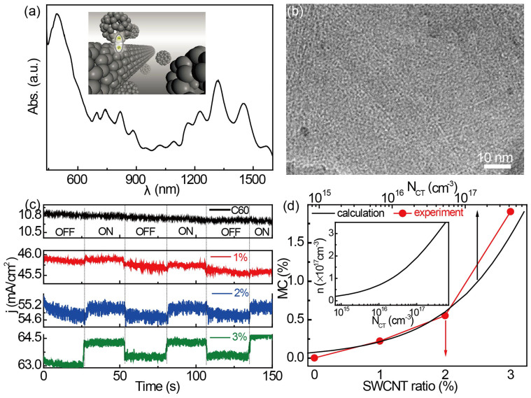
The nano-carbon bulk heterojunction consists of a blend of C60 and SWCNTs. The broad-spectral photoabsorption from the nano-carbon heterojunction at both visible and near-infrared (NIR, Figure 1a) wavelengths creates opportunities for the formation of photoexcited charge-transfer states. From transmission electron microscopy (TEM) images, it is noted that the nano-carbon heterojunction exhibits a random-mixture morphology, as shown in Figure 1b. It should be noted that current density becomes larger when applying a magnetic field in C60-SWCNT heterojunction devices, leading to the positive MC (MC is defined as: MC = [j(B) − j(0)]/j(0), j(B) is current density of the device with magnetic field) value shown in Figures 1c and 1d. The applied magnetic field could induce less spin mixing, which can leads to more triplet charge-transfer20,21. Triplet charge-transfers can further translate into triplet excitons which can also react with free charge carriers due to their long lifetime22,23. The relevant outcome of this type of reaction is the electron and hole separation of triplet excitons24,25, which induces larger carrier density and thus a positive MC. By tuning magnetic field (100 mT) on/off, it is found that the current density of C60-SWCNT nano-carbon devices exhibits the same responsive on/off behavior at room temperature.
Figure 1.
The photoabsorption of the C60-SWCNT nano-carbon (a), the inset of (a) shows the scheme of the C60-SWCNT nano-carbon heterojunction; TEM image of a C60-SWCNT nano-carbon heterojunction, (b) Magnetic field effect in C60-SWCNT heterojunctions with 1 wt%, 2 wt% and 3 wt% SWCNT (c), OFF (ON) means magnetic field is tuned off (on), and B = 100 mT. Theoretical calculation (black line) compared with the experimental result (red circle) (d).
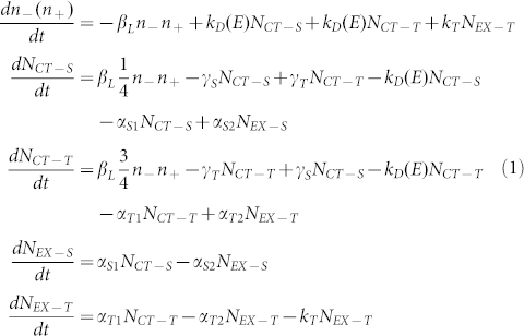
To understand the mechanism of charge-transfer dependent magnetic field effects, theoretical dynamic transition equations21 among electrons, holes, charge-transfers and excitons are built as,
 |
Electron (hole) density n−(n+) is determined by three parts: recombination (βL), dissociation of charge-transfers (kD) and triplet exciton-free charge interaction induced triplet exciton dissociation (kT)9,24,25. The recombination coefficient is βL = e(μ− + μ+)/ε0εr and dissociation rate is  , where J1 is the one order Bessel function and
  , d corresponds to a electron-hole distance of charge-transfers. RC is the Coulomb capture radius, E is electric field, εr the dielectric constant and parameters are: Bhf = a/gμB = 0.1 mT, BJ = J/gμB = 10 mT21, d = 1.3 nm26, RC = 4 nm27. γS and γT in the equation indicate the mutual conversion between singlet (NCT−S) and triplet (NCT−T) charge-transfers, which are determined by the magnetic field (the expressions of γS and γT can be obtained by solving the time dependent Schrodinger Equation21). The transition rate from triplet charge-transfers to singlet ones is expressed as
  , and the rate from singlet charge-transfers to triplet ones is expressed as
  , where ω = gμBB is a parameter which is related to external magnetic field B, a means hyperfine interaction strength and J is exchange interaction strength of charge-transfer. Thus, the magnetic field can tune the ratios of singlet and triplet charge-transfers. Singlet and triplet exciton densities are NEX−S and NEX−T, respectively.
By solving equation (1), the magnetic field dependent carrier density can be obtained. The current density, j = n+eμ+E + n−eμ−E, can be tuned by the magnetic field, which induces magnetic field effects in C60-SWCNT nano-carbon heterojunctions. The carrier density n improves with increasing charge-transfer density NCT, as shown in the inset of Figure 1d. The magnetic field effect becomes more apparent by increasing SWCNT loading ratio, and the MC value can reach as high as 1.9% with 3 wt% SWCNT loading ratio, as shown in Figure 1d. At loadings higher than 3 wt%, the devices become short due to the poor dispersibility of SWCNTs28. The MFE in C60-SWCNT nano-carbon devices is significantly larger than that of previous C60-based devices (MC = 019 and MC = 0.02%18) when the applied magnetic field is 100 mT. In addition, as shown in Figure 1d, our calculation on charge-transfer density dependent MC matches the experimental data well.
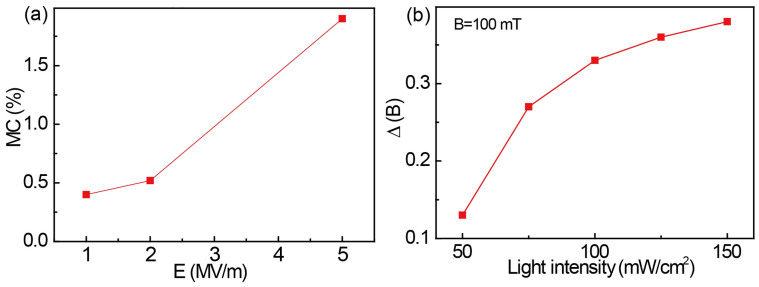
To further study the charge-transfer dependent MC in C60-SWCNT nano-carbon device, we apply different electric field strengths and light intensities to control MFE, as shown in Figures 2a and 2b. By increasing applied electric field, more electrons and holes are injected into the C60-SWCNT nano-carbon active layer. If the distance between electron and hole is smaller than a critical value, the electron and hole will be combined together by Coulomb attraction to form charge-transfer state. In particular, Onsager27,29 proposed a definition for a Coulomb capture radius r at which the Coulomb attraction energy equals the thermal energy kBT:  , e is the elementary charge, εr is the dielectric constant of the surrounding medium, ε0 permittivity of vacuum. The Coulomb attraction radius emphasizes the importance of the dielectric constant of the materials. Due to the small dielectric constant of nano-carbon (εr < 6)30,31, the Coulomb capture radius is large, and charge-transfer states bound by Coulomb attraction are produced with high efficiency. Increasing electron and hole densities will contribute to the formation of a large density of charge-transfer states. Therefore, the MC effect becomes more apparent with a larger electric field, as shown in Figure 2a. In addition to electric field controlled charge-transfer density in C60-SWCNT nano-carbon devices, photoexcitation is also an effective method to excite a large number of charge-transfer states. To measure magnetic field dependent light response in C60-SWCNT nano-carbon devices, we define the optical switch value as: jD = j(on) − j(off), where j(on) and j(off) are electric current densities with and without light illumination, respectively. Figure 2b shows the magnetic field dependent light response:
  under different light intensity and broad-spectrum illumination, where jD(0) = j(on,B = 0) − j(off,B = 0) is the light response without applying magnetic field, and jD(B) = j(on,B) − j(off,B) means the light response under the effect of magnetic field. It is noted that optical switch effect becomes more apparent once applying magnetic field, leading to a positive Δ(B). By further increasing light intensity, more charge-transfer states are excited to enhance the MFE.
Figure 2. The tunability of magnetic field effect by electric field (a) and light intensity, (b) The SWCNT loading ratio is 3 wt% in this case.
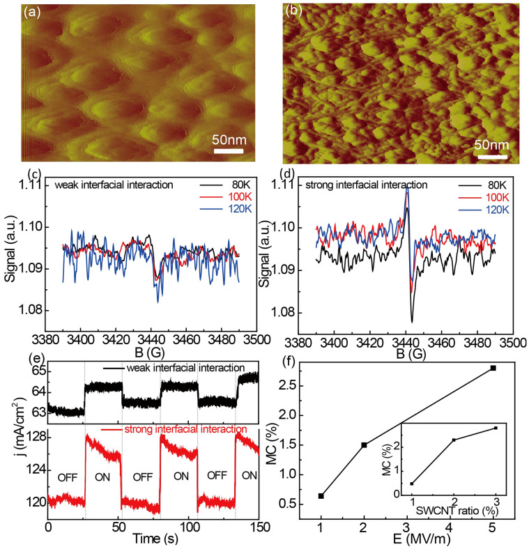
As presented above, the charge-transfer states in C60-SWCNT nano-carbon heterojunctions play an important role in magnetic field effects. In addition, the morphology and interfacial interactions of nano-carbon heterojunctions dictate their charge-transfer process. Therefore, we utilized electron spin resonance (ESR) to further understand the effect of phase separated nano-carbon heterojunctions on charge-transfer induced magnetic field effects. The surface aggregation of C60 and phase segregation with top C60-rich layer is clearly present in the surface morphology of nano-carbon heterojunctions without extended sonication during the C60 and SWCNT blending process (Figure 3a). It should be noted that SWCNTs tend to aggregate in solution to form bundles, which limit the interfacial interaction between SWCNT and C60 within nano-carbon bulk heterojunctions. However, a uniform surface morphology with both C60 and SWCNT is observed after sonication (Figure 3b). The weak ESR signal of nano-carbon heterojunctions without sonication disappeared above 120 K due to limited interfacial interaction [Fig. 3(c)]. Therefore, uniform nano-carbon heterojunction morphology after sonication could enhance the interfacial interaction between C60 and SWCNTs (Figure 3b), leading to a drastically enhanced ESR signal (Figure 3d). Upon increasing the SWCNT ratio to 2 wt% and 3 wt%, the ESR signal is more apparent (Supplementary Information, Figure S4). Temperature dependent ESR signals with different SWCNT ratios are presented in Supplemental Material (Figure S5). It is found that strengthening interfacial interaction by sonication-induced nano-carbon heterojunction could enhance MC (Figure 3e), compared to a low response of the phase segregated one. In addition, the MC effect becomes more apparent with increasing electric field or SWCNT loading ratios on the sonication-processed nano-carbon heterojunctions, as shown in Figure 3f. In particular, by loading 3 wt% SWCNT in C60-SWCNT nano-carbon device, the MC can reach as high as 2.8% at room temperature under 100 mT applied magnetic field.
Figure 3.
Atomic force microscopy image of C60-SWCNT blends with weak interfacial interaction (a) and strong interfacial interaction, (b) ESR signal with 1% SWCNT loading ratio in weak interfacial interaction nano-carbon heterojunctions (c) and strong interfacial interaction nano-carbon heterojunctions (d). Magnetic field effects with strong and weak interfacial interaction (e), OFF (ON) means magnetic field is tuned off (on). (f) Electric field (SWCNT ratio is 3 wt%) and SWCNT ratio dependent MC in strong interfacial interaction nano-carbon heterojunctions.
Discussion
Charge-transfer dependent magnetic field effects are presented for the first time in C60-SWCNT nano-carbon heterojunctions. The singlet and triplet ratios of C60-SWCNT nano-carbon heterojunctions can be tuned by external magnetic field, leading to pronounced magnetic field effects. By tuning charge-transfer density through control of the SWCNT loading ratios, 1.9% of magnetoconductance is achieved with 3 wt% SWCNT loading ratio under 100 mT magnetic field at room temperature, in agreement with theoretical calculations. To further investigate the effect of charge-transfer on magnetic field effects, electric field and light illumination are used to control charge-transfer density in nano-carbon heterojunctions. In addition, by increasing interfacial interactions of C60-SWCNT nano-carbon heterojunctions through morphology and phase separation control, the magnetoconductance is further improved to 2.8% under 100 mT magnetic field at room temperature.
Method
Device structure
Indium tin oxide (ITO) was chosen as the transparent bottom electrode. After cleaning the ITO substrate, Poly(3,4-ethylenedioxythiophene) Polystyrene sulfonate (PEDOT:PSS) was coated at 3500 rpm for 1 minute. Semiconducting SWCNTs were prepared by density gradient ultracentrifugation from raw HiPCo as previously described32. The resulting aqueous dispersions were characterized for semiconducting purity. Surfactants were removed from the SWCNTs by flocculating in ethanol, filtering onto a nylon membrane, and rinsing the membrane in acetone and IPA33. The resulting dry film was weighed and retained for later use. The active layer consists of C60-SWCNT (the concentration of the C60 solution is 30 mg/mL in 1,2-Dichlorobenzene and the SWCNT concentration is 2 mg/mL), which was spun-cast at 1000 rpm for 1 minute. Aluminum was chosen as the top electrode through thermal evaporation. The device area was defined as 0.65 × 1.75 mm2.
Photoabsorption
A Shimadzu UV-3600 spectrophotometer was used to measure the absorption spectrum of the C60-SWCNT nano-carbon heterojunction.
Low temperature ESR measurement
The mixed C60 and SWCNT solution was stirred for 10 hours at room temperature (SWCNT ratios are 1 wt%, 2 wt% and 3 wt%). 150 μL of the C60-SWCNT solution was injected into the glass tube under N2 environment. The low temperature ESR measurement was done under the average of 10 sweeps.
j-V measurement
A Keithley 2400 source generator was used to measure j-V of the C60-SWCNT heterojunction devices in a nitrogen atmosphere glovebox.
Author Contributions
W.Q. did the experimental measurements. S.R. guided the research. S.R. and W.Q. prepared manuscript. M.G. took the TEM images. T.S. and M.C.H. investigated the SWCNT materials, and contributed to the manuscript. All authors contributed to data analysis and discussions.
Supplementary Material
Supplemental Information
Acknowledgments
S.R. thanks the financial support from the Army Research Office - Young Investigator Award (W911NF-14-1-0443) for nanocarbon self-assembly and optoelectronics, and US Department of Energy award (DE-FG02-13ER46937) for organic magnetic study. M.C.H. acknowledges funding from the National Science Foundation (DMR-1006391). T.S. is supported by a National Science Foundation Graduate Research Fellowship and the ANSER Center, an Energy Frontier Research Center funded by the U.S. Department of Energy, Office of Science, Office of Basic Energy Sciences, under Award Number DE-SC0001059.
References
- Baker W. J. et al. Robust absolute magnetometry with organic thin-film devices. Nat. Commun. 3, 898 (2012). [DOI] [PMC free article] [PubMed] [Google Scholar]
- Raman K. V. et al. Interface-engineered templates for molecular spin memory devices. Nature 493, 509–513 (2013). [DOI] [PubMed] [Google Scholar]
- Bloom F. L., Wagemans W., Kemerink M. & Koopmans B. Separating positive and negative magnetoresistance in organic semiconductor devices. Phys. Rev. Lett. 99, 257201 (2007). [DOI] [PubMed] [Google Scholar]
- Bloom F. L., Wagemans W., Kemerink M. & Koopmans B. Correspondence of the sign change in organic magnetoresistance with the onset of bipolar charge transport. Appl. Phys. Lett. 93, 263302 (2008). [Google Scholar]
- Nguyen T. D., Gautam B. R., Ehrenfreund E. & Vardeny Z. V. Magnetoconductance response in unipolar and bipolar organic diodes at ultrasmall fields. Phys. Rev. Lett. 105, 166804 (2010). [DOI] [PubMed] [Google Scholar]
- Francis T. L., Mermer Ö., Veeraraghavan G. & Wohlgenannt M. Large magnetoresistance at room temperature in semiconducting polymer sandwich devices. New J. Phys. 6, 185 (2004). [Google Scholar]
- Wang F. J., Bässler H. & Vardeny Z. V. Magnetic field effects in π-conjugated polymer-fullerene blends: evidence for multiple components. Phys. Rev. Lett. 101, 236805 (2008). [DOI] [PubMed] [Google Scholar]
- Xie Y. et al. Broad-spectral-response nanocarbon bulk-heterojunction excitonic photodetectors. Adv. Mater. 25, 3433–3437 (2013). [DOI] [PMC free article] [PubMed] [Google Scholar]
- Hu B., Yan L. & Shao M. Magnetic-field effects in organic semiconducting materials and devices. Adv. Mater. 21, 1500–1516 (2009). [Google Scholar]
- Wagemans W., Bloom F. L., Bobbert P. A., Wohlgenannt M. & Koopmans B. A two-site bipolaron model for organic magnetoresistance. J. Appl. Phys. 103, 07F303 (2008). [Google Scholar]
- Bobbert P. A., Nguyen T. D., Van-Oost F. W. A., Koopmans B. & Wohlgenannt M. Bipolaron mechanism for organic magnetoresistance. Phys. Rev. Lett. 99, 216801 (2007). [DOI] [PubMed] [Google Scholar]
- Majumdar S. et al. Role of electron-hole pair formation in organic magnetoresistance. Phys. Rev. B 79, 201202 (2009). [Google Scholar]
- Bagnich S. A., Niedermeier U., Melzer C., Sarfert W. & Seggern H. V. Electron-hole pair mechanism for the magnetic field effect in organic light emitting diodes based on poly(paraphenylene vinylene). J. Appl. Phys. 106, 113702 (2009). [Google Scholar]
- Desai P. et al. Magnetoresistance and efficiency measurements of Alq3 based OLEDs. Phys. Rev. B 75, 094423 (2007). [Google Scholar]
- Desai P., Shakya P., Kreouzis T. & Gillin W. P. Magnetoresistance in organic light-emitting diode structures under illumination. Phys. Rev. B 76, 235202 (2007). [Google Scholar]
- Kim G. T. et al. Magnetoresistance of an entangled single-wall carbon-nanotube network. Phys. Rev. B 58, 16064–16069 (1998). [Google Scholar]
- Fedorov G. et al. Magnetically induced field effect in carbon nanotube devices. Nano Lett. 7, 960–964 (2007). [DOI] [PubMed] [Google Scholar]
- Gautam B. R., Nguyen T. D., Ehrenfreund E. & Vardeny Z. V. Magnetic field effect spectroscopy of C60-based films and devices. J. Appl. Phys. 113, 143102 (2013). [Google Scholar]
- Nguyen T. D., Sheng Y., Wohlgenannt M. & Anthopoulos T. D. On the role of hydrogen in organic magnetoresistance: A study of C60 devices. Synth. Met. 157, 930–934 (2007). [Google Scholar]
- Janssen P. et al. Tuning organic magnetoresistance in polymer-fullerene blends by controlling spin reaction pathways. Nat. Commun. 4, 2286 (2013). [DOI] [PubMed] [Google Scholar]
- Qin W., Gao K., Yin S. & Xie S. J. Investigating the magnetic field effect on electron-hole pair in organic semiconductor devices. J. Appl. Phys. 113, 193901 (2013). [Google Scholar]
- Baldo M. A. et al. Highly efficient phosphorescent emission from organic electroluminescent devices. Nature 395, 151–154 (1998). [Google Scholar]
- Wang F., Dukovic G., Brus L. E. & Heinz T. F. Time-resolved fluorescence of carbon nanotubes and its implication for radiative lifetimes. Phys. Rev. Lett. 92, 177401 (2004). [DOI] [PubMed] [Google Scholar]
- Wittmer M. & Zschokke-Gränacher I. Exciton-charge carrier interactions in the electroluminescence of crystalline anthracene. J. Chem. Phys. 63, 4187–4194 (1975). [Google Scholar]
- Hu B. & Wu Y. Tuning magnetoresistance between positive and negative values in organic semiconductors. Nat. Mater. 6, 985–991 (2007). [DOI] [PubMed] [Google Scholar]
- Mihailetchi V. D., Koster L. J. A., Hummelen J. C. & Blom P. W. M. Photocurrent generation in polymer-fullerene bulk heterojunctions. Phys. Rev. Lett. 93, 216601 (2004). [DOI] [PubMed] [Google Scholar]
- Clarke T. M. & Durrant J. R. Charge Photogeneration in organic solar cells. Chem. Rev. 110, 6736–6767 (2010). [DOI] [PubMed] [Google Scholar]
- Bernardi M. et al. Nanocarbon-based photovoltaics. ACS Nano 6, 8896–8903 (2012). [DOI] [PubMed] [Google Scholar]
- Onsager L. Initial recombination of ions. Phys. Rev. 54, 554–557 (1938). [Google Scholar]
- Kataura H. et al. Dielectric constants of C60 and C70 thin films. J. Phys. Chem. Solids 58, 1913–1917 (1997). [Google Scholar]
- Araujo P. T., Jorio A., Dresselhaus M. S., Sato K. & Saito R. Diameter dependence of the dielectric constant for the excitonic transition energy of single-wall carbon nanotubes. Phys. Rev. Lett. 103, 146802 (2009). [DOI] [PubMed] [Google Scholar]
- Green A. A. & Hersam M. C. Nearly single-chirality single-walled carbon nanotubes produced via orthogonal iterative density gradient ultracentrifugation. Adv. Mater. 23, 2185–2190 (2011). [DOI] [PubMed] [Google Scholar]
- Shastry T. A., Morris-Cohen A. J., Weiss E. A. & Hersam M. C. Probing carbon nanotube–surfactant interactions with two-dimensional DOSY NMR. J. Am. Chem. Soc. 135, 6750–6753 (2013). [DOI] [PubMed] [Google Scholar]
Associated Data
This section collects any data citations, data availability statements, or supplementary materials included in this article.
Supplementary Materials
Supplemental Information


