Abstract
A non-complicated, controllable method of metallic nanoparticle fabrication at low operating light power is proposed. The method is based on laser-induced forward transfer, using a metamaterial absorber as the donor to significantly enhance the photothermal effect and reduce the operating light fluence to 35 mJ/cm2, which is much lower than that in previous works. A large number of metallic nanoparticles can be transferred by one shot of focused nanosecond laser pulses. Transferred nanoparticles exhibit good size uniformity and the sizes are controllable. The optical properties of transferred particles are characterized by dark-field spectroscopy and the experimental results agree with the simulation results.
Fabrication of metallic nanostructures has drawn much attention in recent years because of its importance in applications in various fields such as optics, chemistry, microelectronics, biomedicine, etc.1,2,3,4,5,6,7,8,9. The laser-induced forward transfer (LIFT), as one of the methods, has been extensively studied due to its ability to deposit nanostructures of diverse materials onto different receiver substrates10,11,12,13,14,15,16,17,18,19,20,21,22,23,24. However, in previous works, femtosecond laser is typically utilised10,11,12,13,14,15,16,17,18,19,20, while only a few of them are realised by nanosecond laser pulses21,22,23,24. Due to the high melting point of noble metals that are commonly used (bulk Au 1337K, bulk Ag 1235K, etc.), high operating light power is also required. The reported threshold light fluences for metal transferring mostly varied from about 100 mJ/cm2 to several J/cm211,12,13,14,15,16,17,18,19,20,21,22,23, while for those with fluence under 100 mJ/cm2, fs-pulse laser is utilised10. Furthermore, only one nanoparticle (NP)12,13,14,15,16,17,18,19,20,21 or a few NPs without regular morphologies11 are transferred by one light shot in most previous reports. Large-scale transferring methods are rarely studied10,23. In their works, fs-pulse lasers10 or ns-pulse lasers with large fluence (460 mJ/cm2)23 are needed, respectively.
In this article we report a non-complicated method of large-scale gold NPs fabrication through nanosecond laser pulses at low operating fluence based on LIFT. A metamaterial absorber sample is utilised as the donor substrate. The absorber performs nearly perfect absorption at specific wavelength25,26, thus significantly enhancing the photothermal effect around the exposed area. Therefore, the transferring can be realised by ns-pulse lasers with the threshold light fluence reduced to only 35 mJ/cm2. A large number of NPs are transferred by only one light shot. These NPs show good size uniformity and the sizes can be pre-designed due to the mass conservation during the transferring process. Further studies of the transferred NPs are conducted through dark-field spectroscopy, scanning electron microscope (SEM) and transmission electron microscope (TEM). It is found that the properties are comparable to those of Au NPs prepared by chemical methods, as can be confirmed by our numerical simulations.
Experimental section
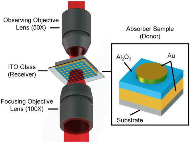
In our experiment, a metamaterial absorber is used as the donor substrate in order to utilise its high absorption to enhance the photothermal effect, thus significantly reducing the operating light fluence. The metamaterial absorber is a three-layer metal-insulator-metal structure, consisting of periodic Au nano-disk (ND) arrays (top) and a continuous Au film (bottom) separated by a Al2O3 layer, as shown in the inset of Fig. 1. Thicknesses of the three layers from top to bottom are 30 nm, 18 nm and 80 nm, respectively. The absorber displays a high-efficient absorption for a specific wavelength. A series of absorber samples are used in our experiment with the ND diameters varied from 50 nm to 350 nm and periods varied from 200 nm to 550 nm. The absorbers are fabricated on quartz substrates with standard nanofabrication techniques25,26. A glass coated with an ITO film is used as the receiver substrate, for its convenience in observing the transferred gold NPs under SEM.
Figure 1. Schematic picture of the transferring experimental setup; the inset shows a single unit of the three-layer metal-insulator-metal absorber structure.
As shown in Fig. 1, the absorber sample is placed upside down with the receiver substrate directly attached underneath. The light source is a super continuum laser (NKT SuperK Compact) with operating wavelengths from 500 nm to 2400 nm, a single-pulse energy of 2 μJ and a pulse width of 3 ns. The light beam, which is normally irradiated on the front side of the absorber sample through the receiver, is collimated and then focused by a 100× objective lens (Mitutoyo, M Plan Apo NIR), with a beam width of about 3 μm.
Due to the high optical absorption by the metamaterial absorber, abundant heat accumulates around the exposed area, resulting in temperature rising above the melting point of Au NDs27. Therefore, the Au NDs in this area are melted and then coalesce into sphere nano-droplets. Within the reshaping process, the particles' centers of gravity move toward the receiver substrate, thus providing the particles with a momentum towards the receiver. Because of the inertia and force of gravity, the droplets are ejected out of the absorber sample and fly onto the receiver substrate24. The transferred nano-droplets cool down and solidify again into spherical dome shapes. Consequently, the laser induced nanoparticle transfer is realised. Owing to the absorber's high-efficient absorption, the operating light fluence is greatly reduced to only 35 mJ/cm2.
Results
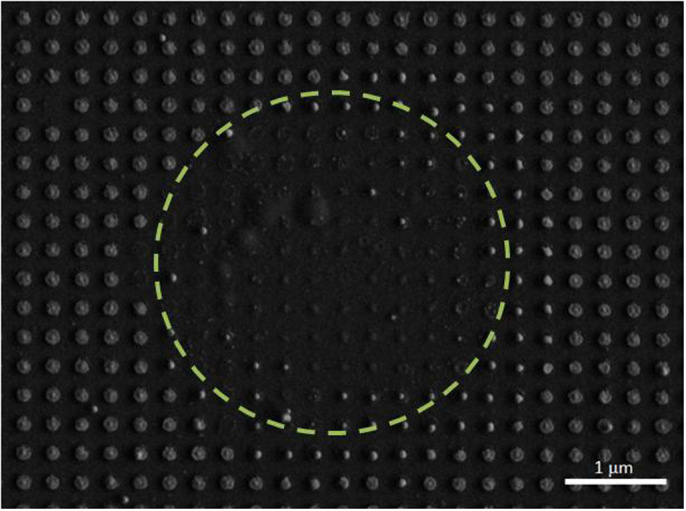
The absorber sample after transferring is characterized under SEM, as shown in Fig. 2. A clear circle is created by one shot, and the diameter of the circle is roughly the same as that of the light beam. The gold NDs inside the circle are transferred. Outside the circle, the light power is not high enough to melt the NDs, so they remain the original disk morphology. Additionally, around the edge light power is sufficient to melt the NDs but not adequate to transfer them, thus leaving the spherical dome shaped NPs on the absorber sample27. Because the period of the NDs is much smaller than the diameter of the circle, many NPs are transferred by only one shot, greatly enhancing the fabrication efficiency.
Figure 2. Top view of the SEM image of an absorber sample after light exposure.

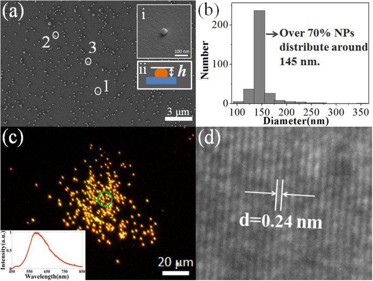
The SEM image of the transferred NPs is provided in Fig. 3(a). Hundreds of NPs are transferred by several light shots. The transferred NPs are randomly positioned on the receiver substrate. This is mainly because of the air disturbance. The whole experiment is not conducted in vacuum; therefore, the air between the donor and receiver substrate can disturb the landing positions of the melted NPs. However, some little migrations of the NPs occurring during the melting process will also affect the positioning. Because the transferred NPs collide with the receiver substrate during the transferring process, they exhibit spherical dome shapes, just like a sphere hewn on the bottom, as shown in inset (ii) of Fig. 3(a), where h represents the height of the NP; the transferred NPs are also observed under SEM of 60° oblique viewing (inset (i) of Fig. 3(a)) to measure their heights. From the size distributions in Fig. 3(b), we can see that most transferred NPs show diameters of around 145 nm from the absorber with the ND diameter of 270 nm and the period of 350 nm, demonstrating the size uniformity of the transferred NPs. A typical dark-field microscopic picture is provided in Fig. 3(c). Bright spots with the similar colour can be observed, and the scattering spectrum of the NPs (the green circle represents the area measured) is shown in the inset and no obvious inhomogeneous broadening could be seen, also indicating the good size uniformity.
Figure 3. The transferred NPs are studied through dark-field spectroscopy, SEM and TEM.
(a) SEM image of receiver substrate; inset (i) is a 60° oblique viewing of a single transferred NP; inset (ii) is the schematic of a single transferred NP, exhibiting a spherical dome shape; here h represents the height of the NP. (b) Histogram of the transferred NP size distribution. (c) Dark-filed optical microscopy image; inset is the scattering spectrum of the NPs, and the area measured is shown by the green circle. (d) A transferred Au NP under TEM.
Discussion
Given the fact that the duration of one laser pulse is only nanosecond and the light power irradiated on the absorber sample is relatively low, gold sublimation does not occur28 and mass conservation of gold can be assumed. For a single transferred NP with h measured to be about 132 nm and diameter of 145 nm, the calculated volume is about 1.59 × 10⁻³ μm3, just slightly smaller than that (1.71 × 10⁻³ μm3) of the Au ND with a 270 nm diameter before transferring. It can also be found that few NPs appear rather bigger than others. Take these particles labeled as 1, 2 and 3 in Fig. 3(a) for example, their diameters are 212 nm, 232 nm and 251 nm, respectively. The corresponding volumes are about 4.87 × 10⁻³ μm3, 6.38 × 10⁻³ μm3 and 8.08 × 10⁻³ μm3, which are nearly 3, 4 and 5 times that of a single particle, respectively. This is due to the fact that several melted gold NPs can merge together and then solidify into a larger sphere during the process of transferring. According to these calculations, mass conservation is satisfied during the transferring process and this ensures that the transferred NPs' sizes can be controlled by designing the parameters of the original NDs. The two related varied parameters of NDs are the diameter and the period. The sizes of transferred NPs are mostly defined by the diameters of NDs, while periods only affect the distribution density of transferred NPs, which leading to the simplicity in the size controlling.
The TEM image of the re-solidified Au NPs shows a lattice fringe spacing of about 0.24 nm (Fig. 3(d)), indicating the Au crystalline structure with (111) orientation. Additionally, energy spectrum of the transferred NPs is measured under SEM experiments, and the results verify that the particles are gold.
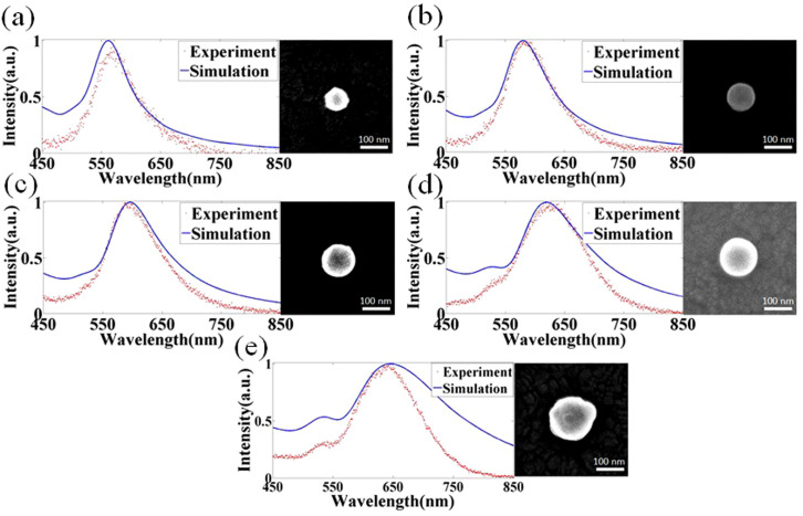
The scattering spectra of single Au NPs are measured by a sensitive spectrometer (Ocean Optics QE65Pro). Here five samples with different transferred NP sizes transferred from five different samples are measured. Scattering spectra and corresponding SEM images are shown in Fig. 4. The diameters of the gold NPs are 86 nm, 115 nm, 135 nm, 148 nm and 172 nm, transferred from NDs with diameters of 120 nm, 180 nm, 230 nm, 265 nm and 330 nm, respectively. As the NP size increases, an obvious red-shift is observed from the measured scattering spectra (red dots), consistent with the simulation results (blue lines) based on finite-difference time-domain method (FDTD Solutions).
Figure 4. Measured (red dots) and simulated (blue lines) scattering spectra and corresponding SEM images of transferred NPs with different sizes.
The diameters are (a) 86 nm, (b) 115 nm, (c) 135 nm, (d) 148 nm and (e) 172 nm, respectively. A distinct red-shift can be observed as the NP size increases.
As mentioned above, the transferred NPs are randomly distributed on receiver and thereby two NPs located extremely close consisting a dimer-like structure can be expected. The scattering spectra of the dimers excited by unpolarized incident light are measured. The dimers show some peculiar properties as compared with a single particle. For a dimer with a ~10 nm spacing between its two singles, its spectrum (red dots and lines) displays a distinct red-shift compared to that of the single NP (blue dots and lines), as demonstrated in Fig. 5(a). When the two singles forming the dimer are not in the same plane, as is shown in the inset of Fig. 5(b), two peaks can be observed in the scattering spectrum. All the experimental results agree well with the simulations.
Figure 5. Scattering spectra of dimers are measured.

(a) Scattering spectra of a dimer (red) and a single NP (blue) are measured (dots) and simulated (lines); and (b) for a dimer with its two singles not in the same plane, two peaks are observed according to the measured (red dots) and simulation (red line) results.
In conclusion, a novel, non-complicated method based on LIFT is proposed to mass-fabricate metal NPs through nanosecond laser pulses at low operating fluence. A metamaterial absorber is utilised as the donor to enhance the photothermal effect. The transferring process can be simply conducted in air, and only a ns-pulse laser operating at low light fluence (35 mJ/cm2) is required. Owing to the high density of NDs on absorber sample, massive NPs can be transferred within one irradiation, and the transferred NPs exhibit excellent size uniformity. Furthermore, since mass conservation is satisfied, the transferred NPs sizes are designable through controlling the original NDs' parameters. The optical properties of transferred single NPs and dimers are measured by dark-field spectroscopy, and the results are consistent with the simulations. Our method is therefore promising in nanostructures preparation for potential optoelectronics and biology applications, in particular, when diameters of NPs is required in advance, while with good uniformity.
Author Contributions
M.Q. conceived the experiment, and supervised the entire project with Q.L. H.M.G. built the experimental setup with the help of X.C. and carried out the characterization with X.X.C. and D.Z. Y.Q.Y. conducted the numerical simulations and analyzed the data with H.M.G. Y.T.C. and M.Y. fabricated the samples. All the authors provided technical and scientific insight and contributed to the writing of the manuscript.
Acknowledgments
This work is supported by the National Natural Science Foundation of China (grants 61275030, 61205030, and 61235007), Qianjiang River Fellow Fund of Zhejiang Province, the Scientific Research Foundation for the Returned Overseas Chinese Scholars from the State Education Ministry, the Opened Fund of State Key Laboratory of Advanced Optical Communication Systems and Networks, the Fundamental Research Funds for the Central Universities, Doctoral Fund of Ministry of Education of China (Grant No 20120101120128)and the Swedish Research Council (VR).
References
- Sun Y. & Xia Y. Shape-controlled synthesis of gold and silver nanoparticles. Science 298, 2176–2179 (2002). [DOI] [PubMed] [Google Scholar]
- González E., Arbiol J. & Puntes V. F. Carving at the nanoscale: sequential galvanic exchange and kirkendall growth at room temperature. Science 334, 1377–1380 (2011). [DOI] [PubMed] [Google Scholar]
- Han W., Li B. & Lin Z. Drying-mediated assembly of colloidal nanoparticles into large-scale microchannels. ACS Nano 7, 6079–6085 (2013). [DOI] [PubMed] [Google Scholar]
- Henzie J., Grünwald M., Widmer-Cooper A., Geissler P. L. & Yang P. Self-assembly of uniform polyhedral silver nanocrystals into densest packings and exotic superlattices. Nat.Mater. 11, 131–137 (2011). [DOI] [PubMed] [Google Scholar]
- Kim S. J., Ah C. S. & Jang D. J. Optical fabrication of hollow platinum nanospheres by excavating the silver core of Ag@Pt nanoparticles. Adv. Mater. 19, 1064–1068 (2007). [Google Scholar]
- Kobayashi M., Seki M., Tabata H., Watanabe Y. & Yamashita I. Fabrication of aligned magnetic nanoparticles using tobamoviruses. Nano Lett. 10, 773–776 (2010). [DOI] [PubMed] [Google Scholar]
- Yan X. M., Contreras A. M., Koebel M. M., Liddle J. A. & Somorjai G. A. Parallel fabrication of sub-50-nm uniformly sized nanoparticles by deposition through a patterned silicon nitride nanostencil. Nano Lett. 5, 1129–1134 (2005). [DOI] [PubMed] [Google Scholar]
- Zhang G., Wang D. & Möhwald H. Ordered binary arrays of Au nanoparticles derived from colloidal lithography. Nano Lett. 7, 127–132 (2007). [DOI] [PubMed] [Google Scholar]
- Ko S. H. et al. Direct nanoimprinting of metal nanoparticles for nanoscale electronics fabrication. Nano Lett. 7, 1869–1877 (2007). [DOI] [PubMed] [Google Scholar]
- Kuznetsov A. I. et al. Laser fabrication of large-Scale nanoparticle arrays for sensing applications. ACS Nano 5, 4843–4849 (2011). [DOI] [PubMed] [Google Scholar]
- Banks D. P., Grivas C., Mills J. D., Eason R. W. & Zergioti I. Nanodroplets deposited in microarrays by femtosecond Ti:Sapphire laser-induced forward transfer. Appl. Phys. Lett. 89, 193107 (2006). [Google Scholar]
- Kuznetsov A. I., Kiyan R. & Chichkov B. N. Laser fabrication of 2D and 3D metal nanoparticle structures and arrays. Opt. Express 18, 21198–21203 (2010). [DOI] [PubMed] [Google Scholar]
- Tseng M. L. et al. Fabrication of plasmonic devices using femtosecond laser-induced forward transfer technique. Nanotechnology 23, 444013 (2012). [DOI] [PubMed] [Google Scholar]
- Papakonstantinou P., Vainos N. A. & Fotakis C. Microfabrication by UV femtosecond laser ablation of Pt, Cr and indium oxide thin films. Appl. Surf. Sci. 151, 159–170 (1999). [Google Scholar]
- Kuznetsov A. I., Koch J. & Chichkov B. N. Laser-induced backward transfer of gold nanodroplets. Opt. Express 17, 18820–18825 (2009). [DOI] [PubMed] [Google Scholar]
- Sametoglu V., Sauer V. & Tsui Y. Y. Nanoscale laser-induced forward transfer through patterned Cr films. Appl. Phys., A Mater. Sci. Process. 110, 823–827 (2013). [Google Scholar]
- Banks D. P., Grivas C., Zergioti I. & Eason R. W. Ballistic laser-assisted solid transfer (BLAST) from a thin film precursor. Opt. Express 16, 3249–3254 (2008). [DOI] [PubMed] [Google Scholar]
- Sametoglu V., Sauer V. T. & Tsui Y. Y. Production of 70-nm Cr dots by laser-induced forward transfer. Opt.Express 21, 18525–18531 (2013). [DOI] [PubMed] [Google Scholar]
- Yang L. et al. Microdroplet deposition of copper film by femtosecond laser-induced forward transfer. Appl. Phys. Lett. 89, 161110 (2006). [Google Scholar]
- Jones C. L. et al. Laser-induced forward-transfer: a rapid prototyping tool for fabrication of photonic devices. Appl. Phys., A Mater. Sci. Process. 101, 333–338 (2010). [Google Scholar]
- Bohandy J., Kim B. F. & Adrian F. J. Metal-deposition from a supported metal-film using an excimer laser. J. Appl. Phys. 60, 1538–1539 (1986). [Google Scholar]
- Willis D. A. & Grosu V. Microdroplet deposition by laser-induced forward transfer. Appl. Phys. Lett. 86, 244103 (2005). [Google Scholar]
- Tseng S. C. et al. Laser-induced jets of nanoparticles: exploiting air drag forces to select the particle size of nanoparticle arrays. Nanoscale 5, 2421–2428 (2013). [DOI] [PubMed] [Google Scholar]
- Habenicht A., Olapinski M., Burmeister F., Leiderer P. & Boneberg J. Jumping nanodroplets. Science 309, 2043–2045 (2005). [DOI] [PubMed] [Google Scholar]
- Hao J. et al. High performance optical absorber based on a plasmonic metamaterial. Appl. Phys. Lett. 96, 251104 (2010). [Google Scholar]
- Hao J., Zhou L. & Qiu M. Nearly total absorption of light and heat generation by plasmonic metamaterials. Phys. Rev. B 83, 165107 (2011). [Google Scholar]
- Chen X., Chen Y., Yan M. & Qiu M. Nanosecond photothermal effects in plasmonic nanostructures. ACS Nano 6, 2550–2557 (2012). [DOI] [PubMed] [Google Scholar]
- Huang W., Qian W. & El-Sayed M. A. Gold nanoparticles propulsion from surface fueled by absorption of femtosecond laser pulse at their surface plasmon resonance. J. Am. Chem. Soc. 128, 13330–13331 (2006). [DOI] [PubMed] [Google Scholar]


