Abstract
As a fundamental electrostatic limit, space charge limit (SCL) for photocurrent is a universal phenomenon and of paramount importance for organic semiconductors with unbalanced photocarriers mobility and high exciton generation. Here we proposed a new plasmonic-electrical concept to manipulate electrical properties of organic devices including photocarriers recombination, transport and collection. As a proof-of-concept, organic solar cells (OSCs) comprising metallic planar and grating electrodes are systematically investigated with normal and inverted device structures. Interestingly, although strong plasmonic resonances induce abnormally dense photocarriers around a grating anode, the grating-inverted OSC is exempt from space charge accumulation (limit) and degradation of electrical properties in contrast to the planar-inverted and planar-normal ones. The particular reason is that plasmonically induced photocarriers redistribution shortens the transport path of low-mobility holes, which are collected by the grating anode. The work demonstrated and explained the SCL breaking with the plasmonic-electrical effect. Most importantly, the plasmonic-electrical concept will open up a new way to manipulate both optical and electrical properties of semiconductor devices simultaneously.
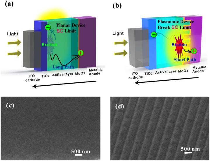
The space charge limit (SCL) effect is a universal phenomenon in semiconductor devices involving light emitting diodes, solar cells, and photodetectors1,2,3,4,5,6,7,8,9. It also sets a fundamental electrostatic limit in electrical properties of organic semiconductor devices with unbalanced photocarriers (electrons and holes) mobility and high exciton generation efficiency10,11,12,13,14. With the interesting features of low cost, low-temperature fabrication, semi-transparency, and mechanical flexibility, organic solar cell (OSC) is currently one of emerging optoelectronic devices and shows a bright outlook for green energy industry12,13,15,16,17,18. Understanding the SCL effect is important to manipulate transport, recombination, and extraction of photocarriers, which will significantly affect the power conversion efficiency (PCE) of OSCs. Typically, the occurrence of SCL4 satisfies the following conditions: (1) unbalanced hole and electron mobility; (2) thick active layer; (3) high light intensity or dense photocarriers (electrons and holes) generation; and (4) moderate reverse bias. Compared to electron mobility, a low mobility of holes typically occurs in organic semiconductor devices depending on fabrication procedures19,20,21,22 e.g. thermal annealing, solvent annealing, etc; and even occurs in the OSCs with robust active materials such as the polymer blend of poly(3-hexylthiophene):[6,6]-phenyl-C61-butyric acid methyl ester (P3HT:PCBM). To investigate SCL characteristics, the inverted OSC with a planar multilayered structure is taken as a representative example. In the planar-inverted OSCs, photocarriers will be generated at the region close to the transparent cathode, such as indium tin oxide (ITO), where incident light will first penetrate. The photogenerated holes with a low mobility will have to transport through the whole active layer, and finally reach the anode (see Figure 1(a)). SCL will occur if the length of active layer is longer than the mean drift length of holes, which is very short because of the low mobility. Meanwhile, holes pile up inside the device to a greater degree than electrons. In other words, positive space charges are accumulated due to the unbalanced photocarriers mobility and a long transport path of holes. As a result, the short-circuit current and fill factor of OSCs will drop significantly due to both the bulk recombination and space charge formation4,7,9,23,24. In this work, we will demonstrate the SCL breaking in the OSCs incorporating metallic (Ag or Au) nanostructures, which offers a novel route to eliminate the SCL effect in semiconductor devices.
Figure 1. A schematic pattern of inverted OSC devices.
(a) inverted OSCs with a planar metallic anode; (b) inverted OSCs with a grating metallic anode. The device structure of the planar-inverted OSC is: ITO (70 nm)/TiO2 (20 nm)/P3HT:PCBM (220 nm)/MoO3 (10 nm)/planar Ag or Au (100 nm); and the device structure of the grating-inverted OSC is: ITO (70 nm)/TiO2 (20 nm)/P3HT:PCBM grating (220 nm)/MoO3 (10 nm)/Ag or Au grating (100 nm). The short notation “SC” denotes the space charge. A long transport path of holes in the planar-inverted OSC induces the SCL characteristics. A short transport path of holes manipulated by the plasmonic-electrical effect in the grating-inverted OSC breaks the SCL. (c) 45°-tilt SEM image of the planar P3HT:PCBM film. (d) 45°-tilt SEM image of the P3HT:PCBM film with the grating structure.
Having unique features of tunable resonances and unprecedented near-field enhancement, plasmon is an enabling technique for light management25,26,27,28. Recently, performances of semiconductor devices (such as thin-film solar cells) have been pronouncedly improved by introducing metallic nanostructures29,30,31,32,33,34,35,36,37,38,39,40,41,42,43,44,45. The improvements are mainly attributed to the plasmonic-optical effects for manipulating light propagation, absorption, and scattering. The plasmonic-optical effects could: (1) boost optical absorption of active materials; (2) spatially redistribute light absorption at the active layer due to the localized near-field enhancement around metallic nanostructures35,46,47. Except for the plasmonic-optical effects, the effects of plasmonically modified recombination, transport and collection of photocarriers, hereafter named plasmonic-electrical effects, have not been explored systematically particularly in organic semiconductors.
In this paper, through the study of plasmonic OSCs, we will show metallic nanostructures go beyond their optical functions to control recombination, transport, and collection of photocarriers generated from active organic materials. Through spatially redistributing light absorption at the active layer, the proposed plasmonic-electrical concept is fundamentally different from the hot carrier effect48,49,50 where photocarriers are generated from metallic nanostructures. The new plasmonic-electrical effect not only lays a physical foundation but also upgrades electrical properties for semiconductor devices. Exploiting both plasmonic-optical and plasmonic-electrical effects via metallic nanostructures will open up a more flexible and integrated way to design high-performance optoelectronic nanodevices.
Results
OSC structures for investigating plasmonically modified SCL characteristics
To intuitively show the plasmonic-electrical effects without involving complicated device structures, we identify and integrate three structural and material configurations into OSCs. 1. Annealed P3HT:PCBM active layer at non-optimized annealing temperature (robust and well-recognized) for unbalanced electron/hole mobility and low hole mobility (to favor SCL effects). 2. Inverted OSC structures for a long hole transport path (to favor SCL effects). 3. Metallic nanograting as an anode shown in Figure 1(b) for demonstrating the plasmonically modified SCL effect. The planar and grating OSCs are inverted device structures of ITO/TiO2 (20 nm)/active layer (220 nm)/MoO3 (10 nm)/Ag or Au (with or without grating) (100 nm). For comparative and systematic study, the planar and grating OSCs with normal device structures of ITO/PEDOT:PSS (30 nm)/active layer (220 nm)/Ca (10 nm)/Ag or Au (with or without grating) (100 nm) are also fabricated. All the active layer thicknesses are about 220 nm. Detailed fabrication of OSCs is shown in Methods Section.
The scanning electron microscope (SEM) images of planar and patterned P3HT:PCBM films are shown in Figures 1(c) and (d). According to the atomic force microscopy (AFM) image, the periodicity and depth of the P3HT:PCBM grating are about 750 nm and 40 nm, respectively (See Supplementary Figure S1). When the Ag or Au anode was subsequently evaporated on the nanostructured active-layer surface, the anode/active layer interface closely follows the surface profile of the active layer. Hence the grating feature was preserved on both Ag and Au anodes.
Elimination of SCL in Ag-grating-inverted (hole-path shortened) OSCs
According to the Mott-Gurney law, by assuming the number of deep localized states is negligible and the mobility is almost field independent, photocurrent (Jph) in the SCL regime can be described by4
 |
where G is the averaged generation rate, Ve is the effective voltage drop across the active layer or hole accumulation region, μh is the hole mobility, q is the electron charge, and ε0εr is the dielectric permittivity of the active layer. Differently, Jph with a sufficiently large reverse bias (recombination is ignorable) is approximated as
 |
where L is the thickness of the active layer. The compensation voltage V0, which is almost equal to the built-in potential of OSCs, is defined as Jph (V0) = 0. The effective applied voltage Ve is given as V0-V, where V is the applied bias voltage.
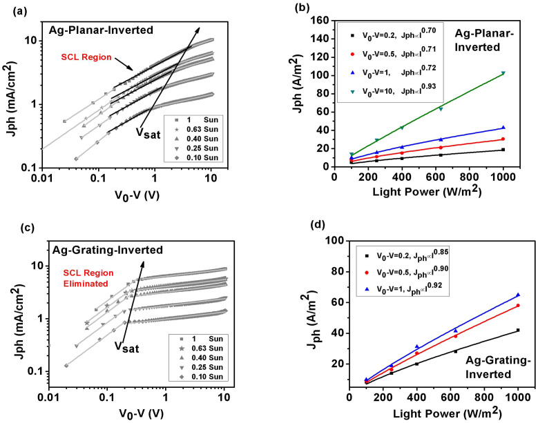
To comparatively study the SCL characteristics in Ag-planar-inverted and Ag-grating-inverted OSCs, we investigated photocurrent Jph under various incident light intensity (I) and effective applied voltage (V0-V) conditions measured at room temperature as shown in Figure 2. For the Ag-planar-inverted device, as shown in Figure 2(a), when V0-V<0.2 V, Jph is almost linearly proportional to V0-V. It is because the dependence of Jph on V0-V at a low internal electrostatic field is governed by both diffusion and drift currents. For intermediate and higher internal fields (see Figure 2(a)), Jph shows a square-root dependence on V0-V covering a wide range of voltages. At sufficiently high reverse voltage, photocurrent becomes saturated (internal-field independent) and no recombination occurs, as the mean distance (w) of free charge carriers becomes equal to or larger than the active layer thickness (L). To verify the SCL occurs in the Ag-planar-inverted OSC, we further plot Jph versus light intensity at three different effective applied voltages (at V0-V = 0.2 V, 0.5 V, 1 V in the square-root regime, and V0-V = 10 V in the saturation regime) as depicted in Figure 2(b). We see that Jph is approximately proportional to I3/4 at the SCL region (1/2 power dependence of Jph on V0-V). Additionally, Jph is approximately proportional to I0.93 at the saturation region for sufficiently high V0-V. According to Equation (1) and SCL theory, we conclude that the space charge effect occurs, which dominates electrical properties of the Ag-planar-inverted device.
Figure 2. SCL characteristics for Ag-inverted OSCs measured at room temperature (T = 300 K).
Left graphs are photocurrents versus effective applied voltage at different incident light intensities. (a) Ag-planar-inverted OSCs, and (c) Ag-grating-inverted OSCs. Light intensity is varied from 100, 63, 40, 25, to 10 mW/cm2 by using neutral density filters. The black solid lines in (a) represent the square-root dependence of photocurrent on effective applied voltage (SCL region). Right graphs are photocurrents versus incident light intensity at different effective applied voltages. (b) Ag-planar-inverted OSCs, and (d) Ag-grating-inverted OSCs.
Regarding the Ag-grating-inverted OSCs, Jph versus V0-V at different incident light intensities is shown in Figure 2(c). Amazingly, we found that the SCL characteristics disappear when a metallic grating anode is incorporated. When V0-V<0.2 V, Jph is almost linearly proportional to V0-V, which is the same as the Ag-planar-inverted device. However, at higher voltages, Jph becomes saturated and shows no square-root dependence on V0-V. Furthermore, with the help of the curve of Jph versus the light intensity at different V0-V (see Figure 2(d)), Jph shows a linear dependence on the light intensity. This suggests the eliminated SCL and reduced bulk recombination.
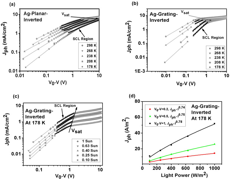
Temperature will strongly affect the mobility of polymer blend and thus SCL characteristics of OSC devices. Regarding the temperature effect, we again study Jph as a function of V0-V for both the Ag-planar-inverted and Ag-grating-inverted OSCs for a temperature range of 178 K-298 K. As shown in Figures 3(a) and (b), the square-root region of Jph will extend to higher voltage regions as temperature decreases for both types of OSCs. Meanwhile, the mobility difference between electrons and holes will be enlarged when temperature decreases (See Supplementary Figure S2 and Figure S3). Especially, at 178 K the mobility ratio (μe/μh) increases to a value of 2000. Thus, an extremely unbalanced transport in these blends is expected. In this case, the SCL will reoccur as depicted in Figures 3(c) and (d).
Figure 3. Experimental temperature-dependent SCL characteristics for Ag-inverted OSCs.
Top graphs are the temperature dependence of photocurrent versus effective applied voltage for (a) Ag-planar-inverted device and (b) Ag-grating-inverted device. Bottom graphs for Ag-grating-inverted device: (c) incident light intensity dependence of photocurrent versus effective applied voltage. (d) effective applied voltage dependence of photocurrent versus incident light intensity. The black solid lines in (a) – (c) represent the square-root dependence of photocurrent on effective applied voltage (SCL region).
Origins of SCL elimination and understanding
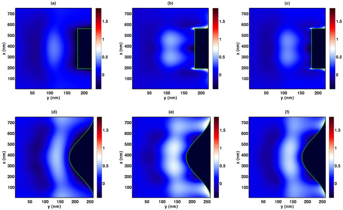
To understand above experimental findings particularly for the SCL elimination in the Ag-grating-inverted OSCs at room temperature, the physical process is theoretically modeled with a mechanistic insight. Through rigorously solving Maxwell's equations51, we calculate the ratio of exciton generation of the Ag-grating-inverted device to that of the Ag-planar-inverted one, which is plotted in Figure 4 (See Supplementary Note 3 for simulation details). Compared to s polarized light which cannot excite plasmons, p polarized light shows a significant enhancement for exciton generation. It was confirmed by the measured polarized absorption ratio (p-polarized absorption over s-polarized absorption and See Supplementary Figure S5) with a plasmonic-boosted peak around 670 nm. Exciton generation for unpolarized sunlight [See Figure 4(c,f)], which is the mean value of the p polarization and s polarization results, shows a very similar distribution pattern to that for the p polarized light [See Figure 4(b,e)]. This proves that plasmonic effects play a dominant role in boosting total exciton generation. The polarization-dependent photoluminescence (PL) spectra (See Supplementary Figure S4) excited by both 355 and 532 nm laser undoubtedly suggest the plasmonic-optical enhancement as well. In view of fabrication pitfalls from the nanoimprinting technique, both a square grating with sharp edges [See Figure 4(a,b,c)] and a sinusoidal grating with smooth edges [See Figure 4(d,e,f)] are modeled to proof the universal optical enhancement by the plasmonic-optical effects. The surface plasmonic band edge (formed by plasmonic standing waves)41 and surface plasmon coupled waveguide mode31 contribute to the exciton hot spots. Most importantly, the extraordinarily dense exciton generation can be found very near to the Ag-grating anode. This suggests near-field plasmonic effects (not far-field scattering effects) play a dominant role in the exciton generation.
Figure 4. Abnormal exciton generation obtained from the theoretical model.
The graphs present the exciton generation of the Ag-grating-inverted devices over that of the Ag-planar-inverted ones, which is defined as log10(Gg(r)/Gp(r)). The active layer thickness for both types of devices is set to be the same. The exciton generation of the Ag-planar device is nonzero at the region corresponding to the nanopatterned anode of the Ag-grating device where zero exciton generation is achieved. (a) s polarization for the square grating; (b) p polarization for the square grating; (c) unpolarization for the square grating; (d) s polarization for the sinusoidal grating; (e) p polarization for the sinusoidal grating; (f) unpolarization for the sinusoidal grating.
As shown in Figure 1(b) and Figure 4, the abnormally redistributed holes (resulting from the dense exciton generation) just transport a short path before collected by the anode. To investigate the influence of the short transport path of holes on electrical properties of OSCs, semiconductor equations (Poisson, drift-diffusion, and continuity equations)52,53,54,55 are solved self-consistently (See Theoretical Model at Methods Section). For the Ag-planar-inverted device, the generation rate of exciton is obtained from a rigorous solution of Maxwell's equations. From Supplementary Figures S6(b) and S8, photocarriers are generated at the region close to the transparent cathode. For the Ag-grating-inverted device, the generation rate is set to
 |
for simulating the nonuniform exciton generation and short transport path of holes. In Equation (3), the Ag-grating anode is located at y = L and  is the mean value of generation rate of the Ag-planar-inverted OSCs. Mathematically, we trivially get
  . Physically, light absorption at the active layer is spatially redistributed in the Ag-grating-inverted OSCs by the localized plasmonic-optical effect.
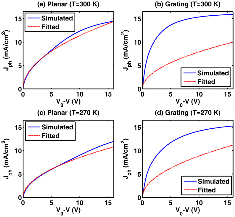
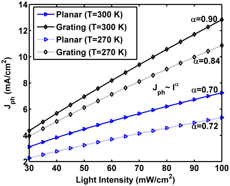
After solving semiconductor equations, Figure 5 shows the dependence of photocurrent Jph on effective applied voltage V0-V. The red solid curves of Jph ~ (V0-V)0.5 are also drawn to identify the SCL regions. At room temperature, the Ag-grating-inverted device is far away from the SCL region while the Ag-planar-inverted device falls into the SCL region extending until 5 V. These results are consistent with the experimental findings as illustrated in Figures. 2(a) and 2(c) [1 Sun case]. As the temperature decreases, the SCL regions dilate for both Ag-planar-inverted and Ag-grating-inverted OSCs, which also has a good agreement with the experimental results by comparing Figures. 2(a, c) to Figures. 3(a, c). At the lower temperature, the simulated Jph curve draws more close to the fitted square-root curve for the Ag-grating-inverted OSCs. Figure 6 shows the dependence of Jph on the light intensity (V0-V is fixed). At room temperature, the order α of 0.9 (Jph ~ Iα) achieved by the Ag-grating-inverted device is fundamentally different from that of 0.7 by the Ag-planar-inverted device, which again verifies the elimination of the SCL characteristics and is identical to the fitted experimental order (See Figures. 2(b, d)). Interestingly, α = 0.9 at the room temperate is reduced to α = 0.84 at the lower temperate (See Figure 6) approaching 3/4 for the Ag-grating-inverted device. The theoretical reduction of α agrees with the experimental demonstrations seen at Figures 2(d) and 3(d). Because the shortened hole transport path cannot compensate the slower drift velocity of holes with a lower mobility. According to our comparative investigations, all the theoretical results are in agreement with experimental findings well.
Figure 5. Theoretical temperature dependence of photocurrent versus effective applied voltage.
(a) Ag-planar-inverted device at T = 300 K; (b) Ag-grating-inverted device at T = 300 K; (c) Ag-planar-inverted device at T = 270 K; (d) Ag-grating-inverted device at T = 270 K. The overlapped regions between fitted and simulated curves are the square-root regions of OSC devices, i.e. Jph ~ (V0-V)0.5. The incident light intensity is 100 mW/cm2.
Figure 6. Theoretical temperature dependence of photocurrent versus light intensity.
The orders α of the curves (Jph ~ Iα) are 0.70, 0.90, 0.72, and 0.84 respectively for Ag-planar-inverted device at T = 300 K, Ag-grating-inverted device at T = 300 K, Ag-planar-inverted device at T = 270 K, and Ag-grating-inverted device at T = 270 K. The effective applied voltage is set to V0-V = 4.0 V.
A short transport path for the Ag-grating-inverted OSCs can be equivalently regarded as a thin active layer configuration for the Ag-planar-inverted OSCs. It is well known that SCL characteristics disappear in the thin-active-layer OSCs (<100 nm)5,24,56. Hence, with the short transport path of holes, the Ag-grating-inverted device does not favor the SCL effect even if it has the same thickness of active layer as the Ag-planar-inverted one where the SCL effect occurs. The shortened transport path leads to a fast collection of holes with reduced bulk recombination and hole accumulation, which can be also observed in the transient photovoltage results (See Supplementary Figure S7). It is worth to note that if the thickness of active layer extensively increases, plasmonic enhancement will become insignificant. Under this situation, few holes are generated around the grating anode and the SCL effect will reoccur (See Supplementary Note 5). Additionally, the enlarged grating anode contact could facilitate the collection of holes, but it does not shorten hole transport paths if the spatial distribution of light absorption at the active layer is unchanged. Consequently, the enlarged anode area is not the physical origin of the eliminated SCL effect.
SCL characteristics in normal (electron-path shortened) OSCs
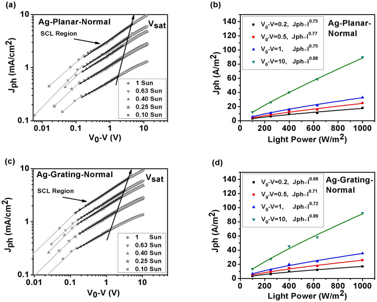
In order to further comprehend the role of transport path in manipulating the SCL characteristics, we fabricated the normal P3HT:PCBM device with structures of ITO/PEDOT:PSS (30 nm)/active layer (220 nm)/Ca (10 nm)/Ag (with or without grating) (100 nm). Differently, in the normal devices, the Ag grating as a cathode for collecting electrons and electrons (not holes) transport a short path before collected by the cathode. For both Ag-planar-normal and Ag-grating-normal devices, we study Jph versus V0-V at different incident light intensities (Figures 7(a) and (c)) and Jph versus light intensity at four different V0-V (Figures 7(b) and (d)). At the square-root region of Jph, photocurrent is approximately proportional to I3/4. Particularly, the Ag-grating-normal device shows the same SCL characteristics at room temperature as what the Ag-planar-normal device does. The short transport path of high-mobility electrons does not reduce charge accumulation and thus SCL still exists. To improve electrical properties of OSCs, the device architecture with metallic nanostructures should be carefully engineered to redistribute light absorption for shortening the transport path of low-mobility photocarriers.
Figure 7. SCL characteristics for Ag-normal OSCs measured at room temperature (T = 300 K).
Left graphs are photocurrents versus effective applied voltage (V0-V) at different incident light intensities. (a) Ag-planar-normal device, and (c) Ag-grating-normal device. The black solid lines in (a) and (c) represent the square-root dependence of photocurrent on effective applied voltage (SCL region). Right graphs are photocurrents versus incident light intensity at different effective applied voltages. (b) Ag-planar-normal device, and (d) Ag-grating-normal device.
Space charge dependent OSC performances
Electrical characteristic parameters of OSCs with four different device structures are listed in Table 1. The corresponding current density-voltage (J-V) curves are given in Supplementary Figure S10 and Figure S11. For the Ag-normal OSCs, the characteristic parameters including short-circuit current (JSC) and fill factor (FF) show no significant distinction for both planar and grating devices. After introducing the nanostructured cathode, the increased JSC and reduced FF are respectively due to the metallic grating enhanced optical absorption and elongated hole (shortened electron) transport path. However, for the Ag-inverted OSCs, the characteristic parameters of the planar and grating devices show considerable differences. For example, FF of the Ag-planar-inverted device drops drastically compared to that of Ag-grating-inverted one. The maximum possible FF at the SCL regime is about 42%4. From results in Table 1, FF of the Ag-planar-inverted and Ag-grating-inverted devices are respectively lower and higher than 42%. The OSCs, which achieve a FF significantly larger than 42%, will be exempt from the SCL. The FF of the Ag-planar-inverted device is noticeably smaller than 42% due to the SCL effect with a large recombination loss. Furthermore, JSC of the Ag-grating-inverted device is improved by 75% in comparison with the Ag-planar-inverted one. On one hand, surface plasmons excited in the metallic grating enhance the optical absorption of OSCs. On the other hand, low-mobility holes, abnormally generated around the grating anode, are collected fast and easily leading to the reduced recombination loss. Hence, the Ag-grating-inverted device improves JSC much more significantly than the Ag-grating-normal one, although the same optical enhancement can be achieved by the Ag-grating-normal device. Considering the improved FF together with the boosted short-circuit current, the PCE of the Ag-grating-inverted device increases from 0.73% to 1.73%.
Table 1. Experimental characteristic parameters of OSCs with different structures. The parameters include open-circuit voltage (VOC), short-circuit current (JSC), fill factor (FF), and power conversion efficiency (PCE).
| VOC | JSC | PCE | ||
|---|---|---|---|---|
| Device | (V) | (mA/cm2) | FF | (%) |
| Ag-Planar-Inverted | 0.61 ± 0.02 | 3.30 ± 0.15 | 0.37 ± 0.02 | 0.73 ± 0.10 |
| Ag-Grating-Inverted | 0.61 ± 0.01 | 5.76 ± 0.28 | 0.56 ± 0.05 | 1.73 ± 0.21 |
| Ag-Planar-Normal | 0.61 ± 0.01 | 2.73 ± 0.25 | 0.44 ± 0.02 | 0.74 ± 0.10 |
| Ag-Grating-Normal | 0.61 ± 0.02 | 2.98 ± 0.21 | 0.41 ± 0.03 | 0.75 ± 0.21 |
SCL Characteristics of Au-grating OSCs
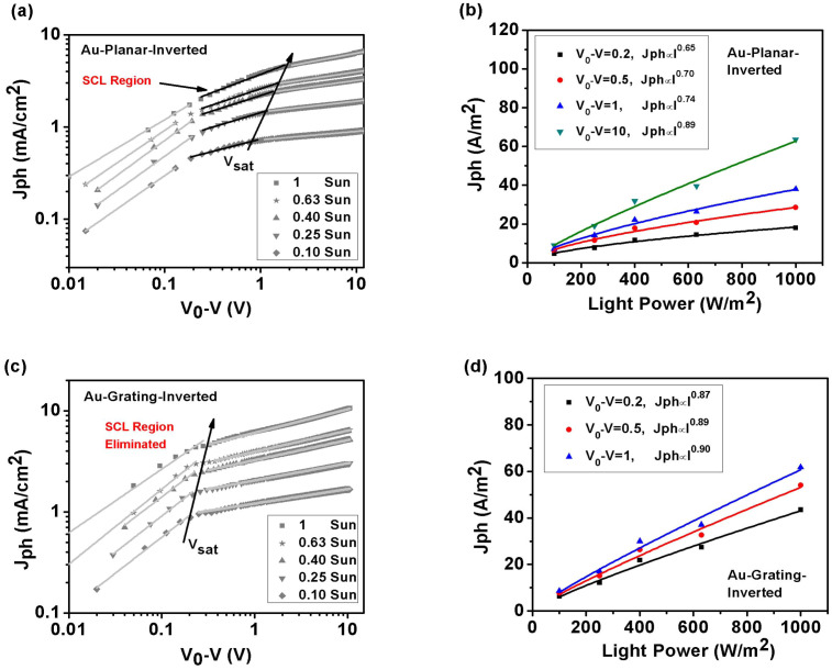
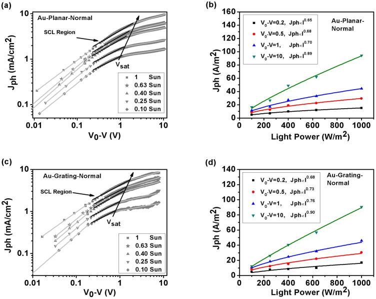
To reconfirm the SCL elimination by the plasmonic-electrical effect, the Au grating has been incorporated into inverted and normal OSCs as the anode and cathode, respectively. Figures 8 and 9 are the corresponding results for the Au-grating devices, which are quite similar to Figures 2 and 7 for the Ag-grating ones. The Au-grating-inverted OSC also avoids SCL due to the same physical reason, i.e. transport path of low-mobility holes is shorten by plasmonically induced light absorption redistribution at the active layer. Likewise, the plasmonic-optical enhancement by the Au grating can be verified by the PL spectra and absorption ratio results at Supplementary Figures S12 and S13. For comparative and complete studies, J-V curves for the Au-planar and Au-grating OSCs are presented in Supplementary Figure S14.
Figure 8. SCL characteristics for Au-inverted OSCs measured at room temperature (T = 300 K).
Left graphs are photocurrents versus effective applied voltage at different incident light intensities. (a) Au-planar-inverted OSCs, and (c) Au-grating-inverted OSCs. Light intensity is varied from 100, 63, 40, 25, to 10 mW/cm2 by using neutral density filters. The black solid lines in (a) represent the square-root dependence of photocurrent on effective applied voltage (SCL region). Right graphs are photocurrents versus incident light intensity at different effective applied voltages. (b) Au-planar-inverted OSCs, and (d) Au-grating-inverted OSCs.
Figure 9. SCL characteristics for Au-normal OSCs measured at room temperature (T = 300 K).
Left graphs are photocurrents versus effective applied voltage (V0-V) at different incident light intensities. (a) Au-planar-normal device, and (c) Au-grating-normal device. The black solid lines in (a) and (c) represent the square-root dependence of photocurrent on effective applied voltage (SCL region). Right graphs are photocurrents versus incident light intensity at different effective applied voltages. (b) Au-planar-normal device, and (d) Au-grating-normal device.
In conclusion, the work experimentally and theoretically demonstrated the plasmonic-electrical effect breaks the SCL in inverted OSCs through introducing a metallic nanostructured anode. The linear dependence of photocurrent on light intensity and significantly improved FF are clear proofs for the eliminated SCL characteristics. Plasmonically induced light absorption redistribution shortens the transport path of low-mobility holes; and thus reduces bulk recombination and space charge accumulation. The proposed plasmonic-electrical concept is helpful to improve the performance of semiconductor devices with active materials of unbalanced mobility. Most importantly, exploring multi-functions of metallic nanostructures offers a new tool to enhance both optical and electrical properties of optoelectronic nanodevices.
Methods
Device fabrication
Devices with inverted structures of ITO/TiO2 (20 nm)/active layer/MoO3 (10 nm)/Ag or Au (with or without grating) (100 nm) and normal structures of ITO/PEDOT:PSS (30 nm)/active layer/Ca (10 nm)/Ag or Au (with or without grating) (100 nm) were fabricated (Figures 1 (a) and (b)). ITO glasses were cleaned based on a standard procedure40,41,43. A thin layer (20 nm) of TiO2 or PEDOT:PSS was formed on the ITO by spin-coating followed by annealing at 150°C for 30 min. Subsequently, a polymer blend of P3HT: PC60BM (1:1, wt%/wt%, 20 mg/ml, note: P3HT in the current work represents Poly[3-hexylthiophene-2,5-diyl] with heavy molecular weight) in Chloroform was spin-coated at 670 rpm for 30 s on top of the TiO2 layer or PEDOT:PSS layer. The active layer thickness is about 220 nm. To obtain the grating pattern on the active layer as shown in Figure 1(b), the polydimethylsiloxane (PDMS) nanoimprinted method was applied onto the surface of active layer40,41,43, after which the whole sample was thermally treated in 80°C for 4 min. By the removal of the PDMS mold, MoO3 (10 nm) or Ca (10 nm) and Ag or Au (100 nm) layers were thermally evaporated onto the active layer pattern at a pressure of 10−6 Torr. Similarly, for the planar control device, the flat PDMS mold was also applied on the active layer. It should be noted the coverage of MoO3 or Ca is used for obtaining an ohmic contact between the Ag or Au electrode and active layer.
Characterization
The thickness of the polymer sample was measured using a Dektak alpha-step profiler. The morphology of the sample was characterized using atomic force microscopy (AFM) (Asylum Research MFP-3D) in tapping mode and scanning electron microscopy (SEM) (Hitachi S-4800). Current density (J)-Voltage (V) characteristics were obtained by using a Keithley 2635 sourcemeter and ABET AM 1.5G solar simulator with 100 mW/cm2 illumination. The low temperature measurement was conducted in an Oxford Cryostat and the incident light intensity was changed from 100 mW/cm2 to 24 mW/cm2 by using a set of neutral density filters.
Theoretical model
The electrical properties of OSCs can be modeled by solving organic semiconductor equations involving Poisson, drift-diffusion and continuity equations52,57
 |
 |
 |
where q is the electron charge, φ is the potential, and n and p are electron and hole densities, respectively. Moreover, μn and μp are the mobility of electrons and holes respectively, which are taken from measurement results (See Supplementary Figures S2 and S3). Furthermore, Dn and Dp are the diffusion coefficients of electrons and holes respectively, which are accessible by the Einstein relations and mobility. Jn = −qμnn∇φ + qDn∇n and Jp = −qμpp∇φ + qDp∇p are respectively electron and hole current densities, and G is the exciton generation rate that is proportional to the incident light intensity. Here, the recombination rate R is taken as the Langevin bimolecular form58. To characterize and understand the SCL effect for photocarriers (i.e., free electrons and holes), we ignored: (1) deep localized states. These states play little role in accumulating space charges; (2) exciton diffusion and dissociation process (described by the exciton diffusion equation and Onsager-Braun theory59,60). Due to the quantum nature of wave functions for polymer materials, most excitons generated in bulk heterojunction OSCs are delocalized to support ultrafast charge transfer61.
The potential boundary condition at the electrodes is given by
 |
where V is the applied bias voltage and Wm is the work function of the electrode. The electrodes are assumed to be ohmic contacts for studying the SCL effect, i.e.
 |
where Nc and Nv are effective density of states for bulk heterojunction active materials.
Author Contributions
W.E.I.S. and X.L. contributed equally to the work. W.C.H.C. planned and supervised the project.
Supplementary Material
SUPPLEMENTARY INFORMATION
Acknowledgments
This work is supported by the General Research Fund (grants: HKU711813 and HKU711612E), the National Natural Science Foundation of China (NSFC)/Research Grants Council (RGC) grant (N_HKU709/12) and Ministry of Education (MOE)/Research Grants Council (RGC) (M-HKU703/12) from RGC of Hong Kong Special Administrative Region, China. This project is also supported in part by Collaborated Research Fund (CUHK1/CRF/12G) of RGC, NSFC grant (No. 61201122), and UGC of Hong Kong (No. AoE/P-04/08).
References
- Goodman A. M. & Rose A. Double extraction of uniformly generated electron-hole pairs from insulators with noninjecting contacts. J Appl Phys 42, 2823–2830 (1971). [Google Scholar]
- Juska G., Viliunas M., Arlauskas K. & Kocka J. Space-charge-limited photocurrent transients-the influence of bimolecular recombination. Phys Rev B 51, 16668–16676 (1995). [DOI] [PubMed] [Google Scholar]
- Koster L. J. A., Mihailetchi V. D., Xie H. & Blom P. W. M. Origin of the light intensity dependence of the short-circuit current of polymer/fullerene solar cells. Appl Phys Lett 87, 203502 (2005). [Google Scholar]
- Mihailetchi V. D., Wildeman J. & Blom P. W. M. Space-charge limited photocurrent. Phys Rev Lett 94, 126602 (2005). [DOI] [PubMed] [Google Scholar]
- Lenes M., Koster L. J. A., Mihailetchi V. D. & Blom P. W. M. Thickness dependence of the efficiency of polymer: fullerene bulk heterojunction solar cells. Appl Phys Lett 88, 243502 (2006). [Google Scholar]
- Dacuna J., Xie W. & Salleo A. Estimation of the spatial distribution of traps using space-charge-limited current measurements in an organic single crystal. Phys Rev B 86, 115202 (2012). [Google Scholar]
- Nicolai H. T. et al. Unification of trap-limited electron transport in semiconducting polymers. Nat Mater 11, 882–887 (2012). [DOI] [PubMed] [Google Scholar]
- Zhang X. G. & Pantelides S. T. Theory of space charge limited currents. Phys Rev Lett 108, 266602 (2012). [DOI] [PubMed] [Google Scholar]
- Di Nuzzo D. et al. Evidence for space-charge-limited conduction in organic photovoltaic cells at open-circuit conditions. Phys Rev B 87, 085207 (2013). [Google Scholar]
- Mihailetchi V. D., Koster L. J. A., Hummelen J. C. & Blom P. W. M. Photocurrent generation in polymer-fullerene bulk heterojunctions. Phys Rev Lett 93, 216601 (2004). [DOI] [PubMed] [Google Scholar]
- Mihailetchi V. D. et al. Charge transport and photocurrent generation in poly (3-hexylthiophene): Methanofullerene bulk-heterojunction solar cells. Adv Funct Mater 16, 699–708 (2006). [Google Scholar]
- Blom P. W. M., Mihailetchi V. D., Koster L. J. A. & Markov D. E. Device physics of polymer: fullerene bulk heterojunction solar cells. Adv Mater 19, 1551–1566 (2007). [Google Scholar]
- Li G., Zhu R. & Yang Y. Polymer solar cells. Nat Photonics 6, 153–161 (2012). [Google Scholar]
- Small C. E. et al. High-efficiency inverted dithienogermole-thienopyrrolodione-based polymer solar cells. Nat Photonics 6, 115–120 (2012). [Google Scholar]
- He Z. C. et al. Enhanced power-conversion efficiency in polymer solar cells using an inverted device structure. Nat Photonics 6, 591–595 (2012). [Google Scholar]
- Guo X. G. et al. Polymer solar cells with enhanced fill factors. Nat Photonics 7, 825–833 (2013). [Google Scholar]
- You J. B. et al. A polymer tandem solar cell with 10.6% power conversion efficiency. Nat Commun 4, 1446 (2013). [DOI] [PMC free article] [PubMed] [Google Scholar]
- Chen H. Y. et al. Polymer solar cells with enhanced open-circuit voltage and efficiency. Nat Photonics 3, 649–653 (2009). [Google Scholar]
- Li G. et al. High-efficiency solution processable polymer photovoltaic cells by self-organization of polymer blends. Nat Mater 4, 864–868 (2005). [Google Scholar]
- Li G. et al. "Solvent annealing" effect in polymer solar cells based on poly(3-hexylthiophene) and methanofullerenes. Adv Funct Mater 17, 1636–1644 (2007). [Google Scholar]
- Azimi H. et al. Charge transport and recombination in low-bandgap bulk heterojunction solar cell using bis-adduct fullerene. Adv Energy Mater 1, 1162–1168 (2011). [Google Scholar]
- Sun Y. M. et al. Inverted polymer solar cells integrated with a low-temperature-annealed Sol-Gel-derived ZnO film as an electron transport layer. Adv Mater 23, 1679–1683 (2011). [DOI] [PubMed] [Google Scholar]
- Wagenpfahl A. et al. S-shaped current-voltage characteristics of organic solar devices. Phys Rev B 82, 115306 (2010). [Google Scholar]
- Kirchartz T. et al. Understanding the thickness-dependent performance of organic bulk heterojunction solar cells: the influence of mobility, lifetime, and space charge. J Phys Chem Lett 3, 3470–3475 (2012). [DOI] [PubMed] [Google Scholar]
- Kawata S. & Shalaev V. M. Nanophotonics with Surface Plasmons. Elsevier (2007). [Google Scholar]
- Maier S. A. Plasmonics: Fundamentals and Applications. Springer. (2007).
- Gramotnev D. K. & Bozhevolnyi S. I. Plasmonics beyond the diffraction limit. Nat Photonics 4, 83–91 (2010). [Google Scholar]
- Schuller J. A. et al. Plasmonics for extreme light concentration and manipulation. Nat Mater 9, 193–204 (2010). [DOI] [PubMed] [Google Scholar]
- Catchpole K. R. & Polman A. Plasmonic solar cells. Opt Express 16, 21793–21800 (2008). [DOI] [PubMed] [Google Scholar]
- Ferry V. E., Sweatlock L. A., Pacifici D. & Atwater H. A. Plasmonic nanostructure design for efficient light coupling into solar cells. Nano Lett 8, 4391–4397 (2008). [DOI] [PubMed] [Google Scholar]
- Pala R. A. et al. Design of plasmonic thin-film solar cells with broadband absorption enhancements. Adv Mater 21, 3504–3509 (2009). [Google Scholar]
- Atwater H. A. & Polman A. Plasmonics for improved photovoltaic devices. Nature Materials 9, 205–213 (2010). [DOI] [PubMed] [Google Scholar]
- Kulkarni A. P. et al. Plasmon-enhanced charge carrier generation in organic photovoltaic films using silver nanoprisms. Nano Lett 10, 1501–1505 (2010). [DOI] [PubMed] [Google Scholar]
- Min C. J. et al. Enhancement of optical absorption in thin-film organic solar cells through the excitation of plasmonic modes in metallic gratings. Appl Phys Lett 96, 133302 (2010). [Google Scholar]
- Sha W., E I., Choy W. C. H., Liu Y. G. & Chew W. C. Near-field multiple scattering effects of plasmonic nanospheres embedded into thin-film organic solar cells. Appl Phys Lett 99, 113304 (2011). [Google Scholar]
- Wu J. L. et al. Surface Plasmonic Effects of Metallic Nanoparticles on the Performance of Polymer Bulk Heterojunction Solar Cells. Acs Nano 5, 959–967 (2011). [DOI] [PubMed] [Google Scholar]
- Yang J. et al. Plasmonic Polymer Tandem Solar Cell. Acs Nano 5, 6210–6217 (2011). [DOI] [PubMed] [Google Scholar]
- Gather M. C. A rocky road to plasmonic lasers. Nat Photonics 6, 708–708 (2012). [Google Scholar]
- John S. Why trap light? Nat Mater 11, 997–999 (2012). [DOI] [PubMed] [Google Scholar]
- Li X. H. et al. Dual Plasmonic Nanostructures for High Performance Inverted Organic Solar Cells. Adv Mater 24, 3046–3052 (2012). [DOI] [PubMed] [Google Scholar]
- Li X. H. et al. Efficient inverted polymer solar cells with directly patterned active layer and silver back grating. J Phys Chem C 116, 7200–7206 (2012). [Google Scholar]
- Spinelli P. et al. Plasmonic light trapping in thin-film Si solar cells. J Opt 14 (2012). [Google Scholar]
- You J. B. et al. Surface plasmon and scattering-enhanced low-bandgap polymer solar cell by a metal grating back electrode. Adv Energy Mater 2, 1203–1207 (2012). [Google Scholar]
- Gan Q. Q., Bartoli F. J. & Kafafi Z. H. Plasmonic-enhanced organic photovoltaics: Breaking the 10% efficiency barrier. Adv Mater 25, 2385–2396 (2013). [DOI] [PubMed] [Google Scholar]
- Li X. H. et al. Efficiency enhancement of organic solar cells by using shape-dependent broadband plasmonic absorption in metallic nanoparticles. Adv Funct Mater 23, 2728–2735 (2013). [Google Scholar]
- Fung D. D. S. et al. Optical and electrical properties of efficiency enhanced polymer solar cells with Au nanoparticles in a PEDOT-PSS layer. J Mater Chem 21, 16349–16356 (2011). [Google Scholar]
- Wang C. C. D. et al. Optical and electrical effects of gold nanoparticles in the active layer of polymer solar cells. J Mater Chem 22, 1206–1211 (2012). [Google Scholar]
- Reineck P. et al. A Solid-State Plasmonic Solar Cell via Metal Nanoparticle Self-Assembly. Adv Mater 24, 4750–4755 (2012). [DOI] [PubMed] [Google Scholar]
- Westphalen M. et al. Metal cluster enhanced organic solar cells. Sol Energy Mater Sol Cells 61, 97–105 (2000). [Google Scholar]
- Zhang D. et al. Plasmonic electrically functionalized TiO2 for high-performance organic solar cells. Adv Funct Mater 23, 4255–4261 (2013). [Google Scholar]
- Sha W. E. I., Choy W. C. H. & Chew W. C. A comprehensive study for the plasmonic thin-film solar cell with periodic structure. Opt Express 18, 5993–6007 (2010). [DOI] [PubMed] [Google Scholar]
- Koster L. J. A., Smits E. C. P., Mihailetchi V. D. & Blom P. W. M. Device model for the operation of polymer/fullerene bulk heterojunction solar cells. Phys Rev B 72 (2005). [Google Scholar]
- Kotlarski J. D. et al. Combined optical and electrical modeling of polymer: fullerene bulk heterojunction solar cells. J Appl Phys 103, 084502 (2008). [Google Scholar]
- Li X. F. et al. Bridging electromagnetic and carrier transport calculations for three-dimensional modelling of plasmonic solar cells. Optics Express 19, A888–A896 (2011). [DOI] [PubMed] [Google Scholar]
- Sha W. E. I., Choy W. C. H., Wu Y. M. & Chew W. C. Optical and electrical study of organic solar cells with a 2D grating anode. Optics Express 20, 2572–2580 (2012). [DOI] [PubMed] [Google Scholar]
- Kotlarki J. D. & Blom P. W. M. Impact of unbalanced charge transport on the efficiency of normal and inverted solar cells. Appl Phys Lett 100, 013306 (2012). [Google Scholar]
- Selberherr S. Analysis and Simulation of Semiconductor Devices. Springer. (1984).
- Langevin P. Recombinaison et mobilites des ions dans les gaz. Ann Chim Phys 28, 433–530 (1903). [Google Scholar]
- Onsager L. Initial recombination of ions. Phys Rev 54, 554–557 (1938). [Google Scholar]
- Braun C. L. Electric-field assisted dissociation of charge-transfer states as a mechanism of photocarrier production. J Chem Phys 80, 4157–4161 (1984). [Google Scholar]
- Heeger A. J. 25th Anniversary Article: Bulk Heterojunction Solar Cells: Understanding the Mechanism of Operation. Adv Mater 26, 10–28 (2014). [DOI] [PubMed] [Google Scholar]
Associated Data
This section collects any data citations, data availability statements, or supplementary materials included in this article.
Supplementary Materials
SUPPLEMENTARY INFORMATION


