Abstract
The total ionizing dose (TID) effects of 60Co γ ray radiation on the resistive random access memory (RRAM) devices with the structure of Ag/AlO x /Pt were studied. The resistance in low resistance state (LRS), set voltage, and reset voltage are almost immune to radiation, whereas the initial resistance, resistance at high resistance state (HRS), and forming voltage were significantly impacted after radiation due to the radiation-induced holes. A novel hybrid filament model is proposed to explain the radiation effects, presuming that holes are co-operated with Ag ions to build filaments. In addition, the thermal coefficients of the resistivity in LRS can support this hybrid filament model. The Ag/AlO x /Pt RRAM devices exhibit radiation immunity to a TID up to 1 Mrad(Si) and are highly suitable for radiation-hard electronics applications.
Keywords: Total ionizing dose (TID) effects, γ ray radiation, RRAM, Hybrid filament model, Filament, Radiation-induced holes
Background
Recently, resistive random access memory (RRAM) has drawn great research attention. It is widely recognized to be a promising nonvolatile memory for the next generation due to its high compatibility with complementary metal-oxide-semiconductor (CMOS) process and outstanding memory performance such as fast switching speed, high storage density, low power consumption, great data reliability, etc [1-7]. In addition, the future application of RRAM in aerospace or nuclear industry is full of potential. The major challenges in such applications lie in the radiation-induced degradation of RRAM performance. Radiation sources in the outer aerospace and nuclear industries include X-ray and γ ray radiation, energetic electrons, protons, and heavy ion bombardment, etc., and they can bring displacement damages, radiation-induced charge trapping on oxide layers, radiation-induced tunneling leakage, soft breakdown, and hard breakdown [8-10]. Some studies have pointed out that a few kinds of RRAM materials have a good immunity to certain types of radiation, such as HfO2[11,12], TiO2[13,14], and Ta2O5[15,16], etc. The reported good radiation immunity can be ascribed to the reversible filament-based switching mechanism of these RRAM devices. When an operation voltage is applied to the RRAM device, metal ions or oxygen ions/vacancies from the device electrodes or from the oxide material, according to the electrical field, drift in the film bulk to form or rupture the conducting filaments, leading the device transit between the high and low resistance states reversibly [17-20]. Similarly, aluminum oxide (AlO x ), which is widely used in modern CMOS technology, also has an excellent filament-based RRAM performance [2,3]. However, the radiation effects on AlO x RRAM are not implemented.
In this work, the filament-based RRAM with the structure of Ag/AlO x /Pt was chosen as the experimental devices since it has the well-understood filament-based switching mechanism. 60Co γ ray treatment is used as the radiation source to investigate the total ionizing dose (TID) effects on the devices. The switching behaviors and memory performances with different radiation doses are compared and analyzed. Moreover, a radiation-induced hybrid filament model is proposed to explain the TID effects of γ ray treatment.
Methods
Ag/AlO x /Pt RRAM devices were fabricated for the radiation study. After a standard Radio Corporation of America (RCA) cleaning of the p-type silicon wafers, a 300-nm-thick silicon dioxide was thermally grown as an isolation layer. Then a 100-nm-thick Pt film was deposited by the e-beam evaporator as a bottom electrode (BE). Next, a 20-nm-thick AlO x film, as resistive switching layer, was deposited by the atomic layer deposition (ALD) at 220°C by using the precursors of trimethylaluminium (TMA) and H2O. After that, a 100-nm-thick Ag film was deposited and patterned by the shadow mask method to form the top electrode (TE). The schematic diagram of the Ag/AlO x /Pt RRAM devices is shown in Figure 1. After the RRAM devices have been fabricated, some of the as-made devices were exposed to 60Co γ ray radiation at the rate of 100 rad(Si)/s with the total dose up to 500 krad(Si) and 1 Mrad(Si). The electrical characteristics of the RRAM devices were measured using an Agilent 1500A precise semiconductor analyzer (Agilent Technologies; Santa Clara, CA, USA) on a variable temperature probe station. The bias was applied at TE, and the BE was connected to ground.
Figure 1.
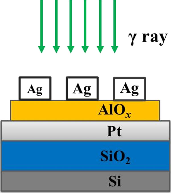
Schematic illustration of the Ag/AlOx/Pt RRAM devices. The 60Co γ ray radiation is performed after the device is fabricated.
Results and discussion
Figure 2 shows the typical current versus voltage (I-V) curves of the Ag/AlO x /Pt RRAM devices with different radiation total dose. A forming process is needed to firstly turn the devices on. All samples exhibit stable bipolar switching behaviors with set and reset voltages at approximately +1.0 and -2.0 V, respectively, so that the switching mode has not been changed by the radiation. The switching mechanism of this kind of RRAM devices has been well studied, which is the formation and rupture of the metallic filaments (Ag) in the oxide film at positive and negative TE bias, respectively [17-20].
Figure 2.
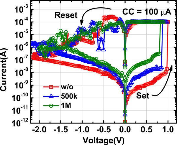
Typical I-V curves of Ag/AlOx/Pt RRAM devices with different total radiation dose. The bipolar resistive switching is still stable after the γ ray radiation.
To investigate the TID radiation impact on the performance of resistive switching memory, at least 15 samples of each RRAM device were measured and analyzed by using a statistical method. Figure 3a shows the initial resistance of the devices, in which an obvious degeneration of uniformity can be found. The resistance reduction of some samples can be observed after the radiation, and the amount of low-resistance samples increases with the radiation dose. It is resulted from the radiation-induced soft breakdown in AlO x film of the RRAM device, and several conducting paths are created by the radiation [21]. As the radiation dose increases, there arise more conducting channels within the film, turning more fresh devices to the low resistance. The initial resistance failure can be recovered by a reset operation through a negative TE bias sweep, bringing the device back to the high resistance state (HRS). Figure 3b presents the distribution of the resistance in HRS and low resistance state (LRS) for the samples. It is reported that holes will be generated by the γ ray in AlO x film, and an increase of tunneling leakage current can be induced by these holes [22]. The resistance at HRS is mainly determined by the resistance of the resistive switching layer [11], so that the increase of leakage paths will lead to the decrease of resistance at HRS. On the other hand, the resistance in LRS is mostly related to the Ag filament. Thus, there is nearly no change of the resistance in LRS after the γ ray radiation.
Figure 3.
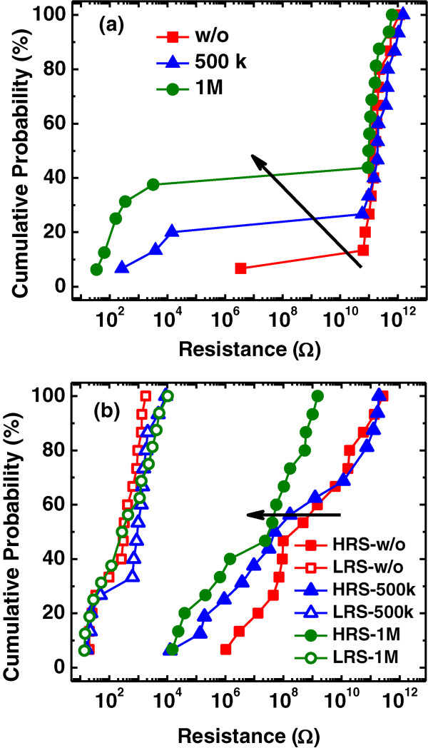
Resistance distributions of the Ag/AlOx/Pt RRAM devices. Distribution of (a) the initial resistance and (b) the resistance in HRS and LRS of the devices with different radiation doses. A degeneration of the initial resistance and the resistance in HRS occurs for the radiated samples.
The distributions of forming voltages and set and reset voltages are demonstrated in Figure 4a and b, respectively. A severe increase to over +10 V of forming voltage is observed for the samples with γ ray radiation, whereas a slight change of set and reset voltages can be observed. For the forming process, the scattering of Ag ions is reinforced by the γ ray radiation and more Ag ions have migrated into the film bulk [11]. Simultaneously, radiation arouses defects and trapped charges inside the film which needs a stronger electrical field to fulfill or recombine. Therefore, a higher forming voltage is needed to realize the first filament gathering and penetration. It is noticeable that the first operation to set the device to LRS is defined as forming process, also for the devices with a low initial resistance and recovered by a reset operation. As for the set process, the radiation-induced holes assist the formation of the Ag filament and result in a slight decrease of set voltage. While for the reset process, the filament rupture is related to the drift of Ag ions under the reset voltage-induced electrical field, therefore the role of the radiation-induced holes can be ignored [11]. Although the radiation leads to a scattering of Ag ions into the film bulk, this scattering influence on the set and reset procedures is almost negligible. After forming operations, several filaments have been built inside the film bulk, and during the following set and reset operations, the rupture and the reconnection of the filaments only occurs within a relatively local region, near the electrode interface.
Figure 4.
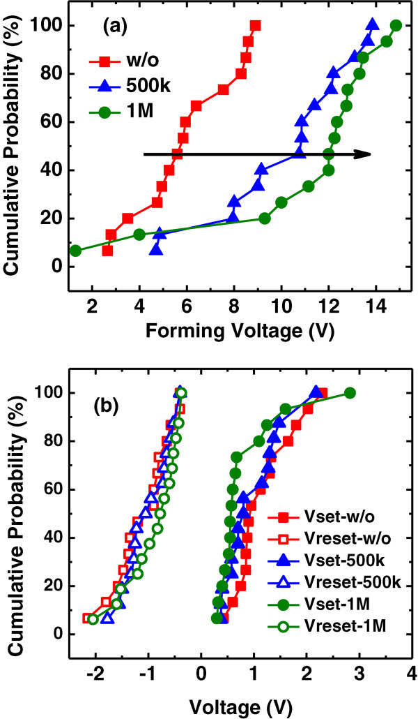
Operation voltage distributions of the Ag/AlOx/Pt RRAM devices. Distribution of (a) the forming voltage and (b) the set and reset voltages with different doses of radiation. An obvious increase in forming voltage and a slight decrease in set voltage are observed.
As the discussion described above, the effects of holes generated by the γ ray radiation are important for the resistive switching of Ag/AlO x /Pt RRAM devices. In order to clarify the role of the radiation-induced holes, an elevated temperature measurement was carried out. The temperature dependence of resistance in LRS of the samples is studied, and the thermal coefficients of resistivity (α) are calculated and shown in Figure 5. The α value of the devices without radiation is extracted to be 0.0041 K-1, which is quite close to the proposed value of 0.0038 K-1 for the high-purity silver at 293 K [23], meaning that the major constituent of conducting filaments in LRS is silver. Interestingly, the α values become smaller as the radiations dose increases, which are 0.0020 and 0.0017 K-1 for the device of 500 krad(Si) and 1 Mrad(Si) dose, respectively. The increase implies that the metal-like characteristic of the filaments changes as the radiation dose increases. The change is due to the holes aroused by γ ray radiation, which co-form the conducting filaments of Ag ions in LRS. Therefore, a hybrid filament model is developed to illustrate the change of RRAM devices after radiation. When the device is exposed to γ ray radiation, electron–hole pairs are generated. Some of the electron-hole pairs recombine, while others drift or hop due to the built-in electric field which is caused by the work function difference between the Ag TE and the Pt BE. During the drift or hopping process, most holes are trapped near the BE interface [15,22]. Figure 6 illustrates the low resistance state (conducting filaments have formed and connected two electrodes) of the devices with different radiation doses. A larger radiation dose brings more holes at the bottom interface. In the set process, when a positive voltage is applied to the TE, Ag ions from TE move towards the BE to form the conducting filament. For the devices with γ ray radiation, the induced holes participate in the growth of filaments and, that is, narrow the distance for Ag ions to drift. Furthermore, the holes create more parallel filaments near the BE interface and a little decrease of set voltage and the resistance in LRS can be observed, as shown in Figures 3b and 4b. As for the reset process, a negative voltage attracts Ag ions back to TE, which is not affected by the holes, so that a little change has been found between these samples. Thus, the constituent of filaments in LRS becomes hybrid after γ ray radiation, which is proved by the thermal coefficients extracted from the resistivity in LRS as shown in Figure 5.
Figure 5.
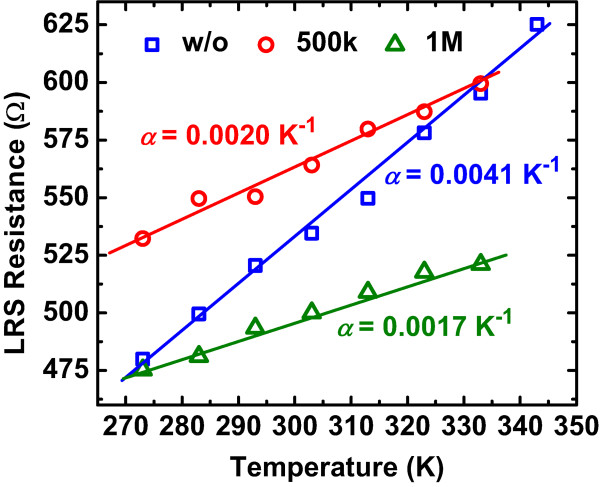
Temperature dependence of resistance in LRS. The symbols are experiment data, and the lines are fitting results. The values of α indicate a change of the metal-like characteristics in filaments as the radiation dose increases.
Figure 6.
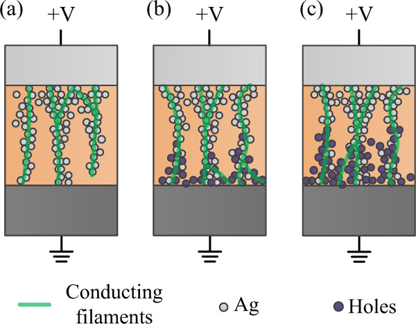
Schematic diagrams of the proposed hybrid filament model for the radiation effects. The schematic diagram of filaments in LRS of the devices (a) without radiation, and with the total radiation dose of (b) 500 krad(Si) and (c) 1 Mrad(Si). The microscopic changes of the filaments reveal an increase of holes generated by the radiation.
Table 1 lists a comparison of the radiation effects between three reported RRAM materials and this work. From the comparison, the RRAM device in this work exhibits a satisfied immunity to high dose γ ray radiation. The degeneration tendency of LRS resistance, HRS resistance, and operation voltages after radiation almost agree with the literature. While the decrease of initial resistance is opposite to the reported result in [15], which is possibly due to the different oxygen-vacancy-governed switching mechanism of TiN/TaO x /Pt devices.
Table 1.
Comparison of radiation effects between published literature and this work
|
References |
Device structure |
Total dose |
Resistance |
Operation voltage |
||||
|---|---|---|---|---|---|---|---|---|
| Initial | Low | High | Forming | Set | Reset | |||
| [11] |
Cu/HfO2:Cu/Pt |
360 krad (Si) |
NA |
√ |
↓ |
√ |
↑ |
√ |
| [13] |
Pt/TiO2/Pt |
14 Mrad (Si) |
NA |
√ |
√ |
NA |
NA |
NA |
| [15] |
TiN/TaO
x
/Pt |
180 krad (Si) |
↑ |
√ |
↓ |
NA |
NA |
NA |
| This work | Ag/AlO x /Pt | 1 Mrad (Si) | ↓ | √ | ↓ | ↑ | √ | √ |
NA, not available; √, no or negligible change; ↑, increase; ↓, decrease.
Conclusions
In this paper, the total ionizing dose (TID) effect of 60Co γ ray radiation on Ag/AlO x /Pt RRAM devices has been investigated. Degradations of uniformity and performance are observed in resistance and switching voltage, which is caused by the radiation-induced holes. A hybrid filament model is proposed to suggest that holes are co-operated with Ag ions to build filaments. The model is proved by the thermal coefficients of resistivity in LRS. Moreover, the Ag/AlO x /Pt RRAM devices demonstrate a satisfactory anti-radiation ability because of the stable resistive switching and a sufficient memory window.
Competing interests
The authors declare that they have no competing interests.
Authors’ contributions
FY and ZZ provide the idea and designed this study. FY performed the experiments under the guidance of JX and LP. J-CW and C-SL participated in the coordination of the study. All authors discussed the results. FY completed the manuscript. All authors read and approved the final manuscript.
Contributor Information
Fang Yuan, Email: yuanf09@mails.tsinghua.edu.cn.
Zhigang Zhang, Email: zgzhang@mail.tsinghua.edu.cn.
Jer-Chyi Wang, Email: jcwang@mail.cgu.edu.tw.
Liyang Pan, Email: panly@mail.tsinghua.edu.cn.
Jun Xu, Email: junxu@mail.tsinghua.edu.cn.
Chao-Sung Lai, Email: cslai@mail.cgu.edu.tw.
Acknowledgements
This work was supported (in part) by the State Key Development Program for Basic Research of China (No. 2011CBA00602) and the National Natural Science Foundation of China (No. 20111300789).
References
- Waser R, Aono M. Nanoionic-based resistive switching memories. Nat Mater. 2007;9:833–840. doi: 10.1038/nmat2023. [DOI] [PubMed] [Google Scholar]
- Wu Y, Lee B, Wong HSP. Al2O3-based RRAM using atomic layer deposition (ALD) with 1-μA RESET current. IEEE Electron Device Lett. 2010;9:1449. [Google Scholar]
- Wong HSP, Lee HY, Yu S, Chen Y-S, Wu Y, Chen P-S, Lee B, Chen FT, Tsai M-J. Metal–oxide RRAM. Proc IEEE. 2012;9:1951. [Google Scholar]
- Prakash A, Maikap S, Chiu H-C, Tien T-C, Lai C-S. Enhanced resistive switching memory characteristics and mechanism using a Ti nanolayer at the W/TaOx interface. Nanoscale Res Lett. 2013;9:288. doi: 10.1186/1556-276X-8-288. [DOI] [PMC free article] [PubMed] [Google Scholar]
- Yuan F, Wang J-C, Zhang ZG, Ye Y-R, Pan LY, Xu J, Lai C-S. Hybrid aluminum and indium conducting filaments for nonpolar resistive switching of Al/AlOx/indium tin oxide flexible device. Appl Phys Express. 2014;9:024204. doi: 10.7567/APEX.7.024204. [DOI] [Google Scholar]
- Chen YY, Goux L, Clima S, Govoreanu B, Degraeve R, Kar GS, Fantini A, Groeseneken G, Wouters DJ, Jurczak M. Endurance/retention trade-off on HfO2/metal cap 1T1R bipolar RRAM. IEEE Trans Electron Devices. 2013;9:1114. [Google Scholar]
- Hsieh M-C, Liao Y-C, Chin Y-W, Lien C-H, Chang T-S, Chih Y-D, Natarajan S, Tsai M-J, King Y-C, Lin CJ. IEEE International Electron Devices Meeting. IEDM Technical Digest: 9–11 December 2013. Washington, DC: Piscataway: IEEE; 2013. Ultra high density 3D via RRAM in pure 28nm CMOS process. 10.3.1. [Google Scholar]
- Srour JR, Marshall CJ, Marshall PW. Review of displacement damage effects in silicon devices. IEEE Trans Nucl Sci. 2003;9:653. doi: 10.1109/TNS.2003.813197. [DOI] [Google Scholar]
- Paccagnella A, Candelori A, Milani A, Formigoni E, Ghidini E, Pellizzer F, Drera D, Fuochi PG, Lavale M. Breakdown properties of irradiated MOS capacitors. IEEE Trans Nucl Sci. 1996;9:2609. doi: 10.1109/23.556843. [DOI] [Google Scholar]
- Miao B, Mahapatra R, Jenkins R, Silvie J, Wright NJ, Horsfall AB. Radiation induced change in defect density in HfO-based MIM capacitors. IEEE Trans Nucl Sci. 2009;9:2916. [Google Scholar]
- Wang Y, Lv H, Wang W, Liu Q, Long S, Wang Q, Huo Z, Zhang S, Li Y, Zuo Q, Lian W, Yang J, Liu M. Highly stable radiation-hardened resistive-switching memory. IEEE Electron Device Lett. 2010;9:1470. [Google Scholar]
- He X, Wang W, Butcher B, Tanachutiwat S, Geer RE. Superior TID hardness in TiN/HfO2/TiN ReRAMs after proton radiation. IEEE Trans Nucl Sci. 2012;9:2550. [Google Scholar]
- Tong WM, Yang JJ, Kuekes PJ, Stewart DR, Williams RS, DeIonno E, King EE, Witczak SC, Looper MD, Osborn JV. Radiation hardness of TiO2 memristive junctions. IEEE Trans Nucl Sci. 2010;9:1640. [Google Scholar]
- DeIonno E, Looper MD, Osborn JV, Palko JW. Displacement damage in TiO2 memristor devices. IEEE Trans Nucl Sci. 2013;9:1379. [Google Scholar]
- Zhang LJ, Huang R, Gao DJ, Yue P, Tang PR, Tan F, Cai YM, Wang YY. Total ionizing dose (TID) effects on TaOx-based resistance change memory. IEEE Trans Nucl Sci. 2011;9:2800. [Google Scholar]
- Hughart DR, Lohn AJ, Mickel PR, Dalton SM, Dodd PE, Shaneyfelt MR, Silva AI, Bielejec E, Vizkelethy G, Marshall MT. A comparison of the radiation response of TaOx and TiO2 memristors. IEEE Trans Nucl Sci. 2013;9:4512. [Google Scholar]
- Kund M, Beitel G, Pinnow CU, Röhr T, Schumann J, Symanczyk R, Ufert KD, Müller G. IEEE International Electron Devices Meeting. IEDM Technical Digest: 5–7 December 2005. Washington, DC: Piscataway: IEEE; 2005. Conductive bridging RAM (CBRAM): an emerging non-volatile memory technology scalable to sub 20 nm. [Google Scholar]
- Kim DC, Seo S, Ahn SE, Suh DS, Lee MJ, Park BH, Yoo IK, Baek IG, Kim HJ, Yim EK, Lee JE, Park SO, Kim HS, Chung UI, Moon JT, Ryu BI. Electrical observations of filamentary conductions for the resistive memory switching in NiO films. Appl Phys Lett. 2006;9:202102. doi: 10.1063/1.2204649. [DOI] [Google Scholar]
- Ninomiya T, Wei Z, Muraoka S, Yasuhara R, Katayama K, Takagi T. Conductive filament scaling of TaOx bipolar ReRAM for improving data retention under low operation current. IEEE Trans Electron Devices. 2013;9:1384. [Google Scholar]
- Liu CY, Huang JJ, Lai CH, Lin CH. Influence of embedding Cu nano-particles into a Cu/SiO2/Pt structure on its resistive switching. Nanoscale Res Lett. 2013;9:1. doi: 10.1186/1556-276X-8-1. [DOI] [PMC free article] [PubMed] [Google Scholar]
- Paccagnella A, Cester A, Cellere G. IEEE International Electron Devices Meeting. IEDM Technical Digest: 13–15 December 2004. San Francisco, CA: Piscataway: IEEE; 2004. Ionizing radiation effects on MOSFET thin and ultra-thin gate oxides; pp. 473–476. [Google Scholar]
- Felix JA, Schwank JR, Fleetwood DM, Shaneyfelt MR, Gusev EP. Effects of radiation and charge trapping on the reliability of high-k gate dielectrics. Microelectron Reliab. 2004;9:563. doi: 10.1016/j.microrel.2003.12.005. [DOI] [Google Scholar]
- Weast RC. CRC Handbook of Chemistry and Physics, Volume 69. Boca Raton, FL: CRC Press; 1988. [Google Scholar]


