

Abstract

The influence of the nature of interface between organic semiconductor and gate dielectric on bias stress electrical stability of n-type C60-based organic field effect transistors (OFETs) was studied. The bias stress induced threshold voltage (Vth) shift was found to depend critically on the OFET device structure: the direction of Vth shift in top-gate OFETs was opposite to that in bottom-gate OFETs, while the use of the dual-gate OFET structure resulted in just very small variations in Vth. The opposite direction of Vth shift is attributed to the different nature of interfaces between C60 semiconductor and Parylene dielectric in these devices. The Vth shift to more positive voltages upon bias stress in bottom-gate C60-OFET was similar to that observed for other n-type semiconductors and rationalized by electron trapping in the dielectric or at the gate dielectric/C60 interface. The opposite direction of Vth shift in top-gate C60-OFETs is attributed to free radical species created in the course of Parylene deposition on the surface of C60 during device fabrication, which produce plenty of hole traps. It was also realized that the dual-gate OFETs gives stable characteristics, which are immune to bias stress effects.
Keywords: C60/Parylene interface, bias stress, n-type OFETs electrical stability, threshold voltage shift, charge trapping, top-gate, bottom-gate and dual-gate OFETs
1. Introduction
In the last two decades, tremendous progress has been made in the development of organic field effect transistors (OFETs). The performance of OFETs has been improved, and now they are comparable to the amorphous silicon transistors.1−3 The applications are foreseen as a driver of flat panel display,4 memory devices,5 smart labels,6 and biological sensor.7,8 The stability of OFETs is a critical requirement for practical applications, but the OFETs are giving unstable characteristics under continuous bias stress.9 The main bias stress induced instability appears as a shift in the threshold voltage (Vth) or as a decrease in drain source current (IDS) at fixed voltage.10 Several efforts were made to measure the bias stress induced instabilities in p-type OFETs,11 but n-type OFETs are still awaiting more attention.12 The major reasons of bias stress instabilities are the charge trapping in the organic semiconductor,13−16 in the gate dielectric,17,18 or at the interface between active layer and dielectric.19,20
The nature of interface between the organic semiconductor and the gate dielectric plays a major role in the charge carrier transport of OFETs.21 In pentacene-based OFETs with an embedded thin layer of copper oxide (CuO), it was found that the trapped electrons at the interface between pentacene and CuO are not easily released, which results in a stable threshold voltage up to 3000 s against the bias stress.22 The threshold voltage stability of OFETs can be related to the energetic distribution of the barrier heights for charge trapping between organic semiconductor and gate dielectric. The relation of bias stress induced Vth shift and trapping energy distribution was analyzed by measuring the temperature dependence of source-drain current decay under gate bias stress. It was noticed that the barrier heights for charge trapping become higher and narrower by using a self-assembled monolayer, resulting in stable transfer characteristics against bias stress without any significant change in Vth.23 The role of a self-assembled monolayer in stabilization of output characteristics was investigated by using different types of self-assembled monolayers in SiO2 insulator-based pentacene OFETs. The results reveal that bias stress induced Vth shift was considerably increased by introducing long chain chemical species on the surface of the insulator, while OFETs with short chain self-assembled monolayers on the surface of SiO2 give characteristics with stable threshold voltage against continuous gate bias stress.24 Most of the studies related to interface and Vth instabilities are done by using bottom-gate top-contact OFETs, while little attention was given to measure the Vth stability of top-gate OFETs.25,26 It has been already found that the deposition technique and the order of deposition of organic semiconductors and gate insulator have a huge influence on the formation of the active interface,27 and the nature of interface has a direct impact on charge carrier transport in OFETs.
To investigate the role of the interface on bias stress induced threshold voltage instabilities, the C60-based top-gate and bottom-gate OFETs with Parylene as a gate dielectric were studied. It was observed that the direction of bias stress induced Vth shift in top-gate OFETs was opposite to the bottom gate OFETs. The investigations were further extended, and experimental results reveal that the use of dual-gate can result in stable characteristics with small variations in Vth with gate bias stress.
2. Experimental Details
For the fabrication of different device geometry OFETs, a 0.5 mm wide and 100 nm thick gate electrode of Aluminum was evaporated on glass substrate by using shadow mask with a background pressure of 10–6 mbar. Parylene was used as dielectric and the deposition was done in a homemade system which has three temperature zones. First, the dimer dichloro-di-p-xylylene is evaporated at a temperature of 100 °C, next the vapor is passing a high temperature zone (750 °C) where pyrolysis leads to cleavage of the dimers. The resulting monomers are finally deposited at room temperature on the sample surface, where they spontaneously polymerize to form a transparent and conformal thin film. The process is carried out at a pressure of 10–2 mbar, and for the bottom-gate OFET fabrication a dielectric layer thickness of 1 μm was used. C60 was used as received from MER Corp. The 150 nm thick organic semiconductor film of C60 was grown by hot-wall epitaxy (HWE) at a substrate temperature Tsub = 100 °C, source temperature Ts = 360 °C, and wall temperature Twall = 400 °C with a background pressure of 10–6 mbar. For top contact electrodes, 70 nm thick Al was evaporated under high vacuum of 10–6 mbar, using a shadow mask. The channel length L and width W in the OFETs were 70 μm and 1.5 mm, respectively. In a similar way (except the order of deposition of C60/Parylene), the top-gate bottom-contacts and dual-gate OFETs were also fabricated. A dual-gate transistor in fact consists of a bottom-gate top-contacts transistor with an additional second gate and second dielectric layer. Device transportation from the fabrication laboratory to measurement laboratory was carried out in a nitrogen-filled box.
All OFETs were characterized at room temperature under N2 atmosphere inside a glovebox, to avoid exposure to ambient humidity and oxygen (both values were maintained below 0.5 ppm). More detail of experimental procedure can be found elsewhere.28,29 For applying the gate voltage (VGS) and measuring the leakage current a Keithley 6487 Pico-Ampere meter with included voltage source was used, whereas the source-drain voltage (VSD) characteristics were recorded by a Keithley 2400 voltage source unit.
The electrical stress was applied to each type device in matrix form. During the bias stress time, the gate voltage was continuously varied from −10 to 50 V in steps of 300 mV, and for each VGS value, the VSD voltage was ramped from 0 to 50 V in steps of 300 mV. In the case of dual-gate OFETs, the same VGS was applied to bottom gate and to gate electrode. All instruments are controlled by a PC, and the acquired data were stored by a MATLAB program.
3. Results and Discussion
To measure the bias stress stability, all three different OFET structures were installed at the measurement setup, one by one. Before applying bias stress, the charge carrier field effect mobility for bottom-gate, top-gate, and dual-gate OFETs was measured to be 0.1, 0.2, and 0.9 cm2 V–1 s–1, respectively. Each OFET was electrically stressed for 125 h, in dark. During the bias stress time, the transfer characteristics were measured from all three different structure based OFETs. The transfer characteristics measured before bias stress, after 24h and 125h of bias stress are presented in Figure 1. The Vth of bottom-gate OFETs was shifted toward more positive voltage (from 20.7 to 34.6 V), while for top-gate OFETs the bias-stress resulted in the Vth shift in opposite direction to the left (from 14.3 to 0.1 V) . In the case of dual-gate OFETs, only a small shift in the Vth (from 11.5 to 8.5 V) was observed.
Figure 1.

Transfer characteristics measured during the continuous bias stress of 125 h (a) bottom-gate top-contacts, (b) top-gate bottom-contacts, and (c) dual-gate OFETs.
To quantify the bias stress instability in all three different geometrical-based OFETs, the Vth was extracted from the transfer characteristics measured during the continuous bias stress time. For all three different geometrical structure based OFETs, the change in the Vth during the continuous bias stress time is presented in Figure 2. The Vth of bottom-gate OFET was changed by 70%, the Vth of top-gate OFET changed by 100%, while the Vth of dual-gate OFET changed by 20% only. The direction of change of Vth in dual-gate OFET was the same as observed in top-gate OFETs. This means that bias stress phenomenon is related to top and bottom interface between C60 and Parylene, because all other device specifications are the same. The improved stability observed in dual-gate OFET provide an evidence that the mitigation of bias stress effects caused by bottom-gate OFETs can be done by applying gate bias stress to the top-gate OFETs and vice versa. In dual-gate OFET, the bias stress induced instability at the top interface is higher than the instability at the bottom interface caused by bias stress, because net direction of threshold voltage shift is similar to the top-gate OFET.
Figure 2.
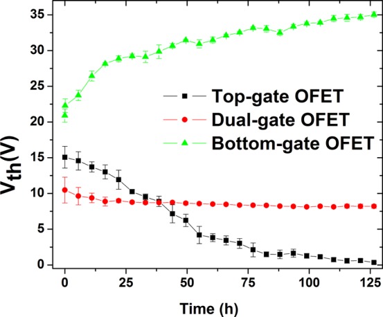
Variation in threshold voltage (Vth) with bias stress time in all three different geometrical structure based OFETs, measured in dark.
For practical application and device modeling, the stability of source-drain current measured at a fixed voltage during the bias stress time is also an important parameter. The on/off current ratio was also extracted from the transfer characteristics measured during the bias stress time and is presented in Figure 3. The degradation in the on/off current ratio of bottom-gate OFETs was larger as compared to top-gate and dual gate OFETs. It is clear, from Figure 3, that dual-gate OFETs also have higher values of on/off ratio as compared to bottom-gate and top-gate OFETs. The performance of dual-gate OFETs is known to be better than in conventional single-gate OFETs.30,35 To measure the experimental reproducibility, four devices of each geometrical configuration (bottom-, top-, and dual-gate OFETs) were electrically stressed with same bias stress conditions and the same behavior was observed in all OFETs tested. Figures 2 and 3 present the mean values of the figures of merit (Vth and on/off current ratio) along with standard deviations depicted by error bars. In the initial stage of the bias stress process the standard deviations from the mean values tend to be larger, which is mainly attributed to the difference in the fabrication process of all these OFETs.
Figure 3.

Variation of on/off current ratio with bias stress time of all three types of OFETs measured in dark.
During continuous bias stress time, the output characteristics of all three types of OFETs were measured and presented in Figure 4. The output characteristics provide the preliminary information, weather this device can be considered for modeling of an electronic circuit design or not. The existence of discrete “guard bands”29,31 in the output characteristics is an important evaluation factor proving that the transistor device can potentially be used for reliable electronic circuits. The guard band means that there are nonoverlapping I–V-curve regions for the different main VGS value steps in the output characteristic, as well as for different main VDS values in the transfer characteristic. Only the dual-gate OFETs clearly depicts well separated guard bands in the output characteristics during the continuous bias stress time, while in top-gate and bottom-gate OFETs the guard bands are not well separated. The threshold voltage instability is the main reason for the absence of guard band in output characteristics of top-gate and bottom-gate OFETs. By comparison of Figure 4a–c, it is easy to understand, that the threshold voltage stability is a major hindrance for OFETs to be considered as a part of future electronic circuits. The guard bands also provide us information about the maximum and minimum values of IDS measured at any value of VGS and VDS. If the guard bands are discrete, then the measured degradation in IDS can be accommodated by applying guard band voltage.29,31
Figure 4.

Output characteristics measured during bias stress time in (a) top-gate, (b) bottom-gate, and (c) dual-gate C60-based OFETs.
We should point out that observation of the bidirectional bias stress induced Vth shift in C60-based OFET depending on device geometry (bottom-gate vs top-gate devices) is puzzling because these devices were prepared in the same environment and deposition conditions, the only difference was the sequence in C60/Parylene layer deposition. The Vth shifts to more positive voltages upon bias stress found in bottom-gate C60-OFET (Figure 1a) can conventionally be rationalized in terms of electron trapping in the dielectric or at the gate dielectric/C60 interface as the electrons are abundantly present in the conductive channel of this OFET. Indeed, as demonstrated by Chua et al.,40 electron trapping is believed to be the main suspect for the shift in Vth in n-type organic transistors. A very similar Vth shift to more positive VGS was already reported for another n-type semiconductor, namely, perylene diimide derivative perylene-3,4,9,10-tetracarboxylic-3,4,9,10-diimide (PTCDI)-C13H27.36
On the other hand, the opposite direction Vth shift in top-gate C60 OFET devices is a rather unexpected effect and requires more detailed consideration. Apparently, Vth shift toward a negative VGS implies accumulation of some metastable positive charges in the vicinity of the interface during the bias stressing. It worth noting that bidirectional Vth shift has been observed in pentacene OFETs36 and was assigned to either hole or electron trapping depending on the bias stress polarity. However, that bidirectional effect was observed only for ambipolar semiconductor films and the Vth shifted in only one direction when semiconductors showed unipolar behaviors as, for instance, in a pentacene OFET exposed to humid air or in PTCDI-C13H27 OFET.36 Note that our OFET devices featured a pure unipolar behavior with no indication on ambipolarity, therefore trapping of injected holes can be ruled out as possible reason for the effect. Another possible reason for the opposite direction Vth shift in top-gate C60 OFET devices can be related to mobile ions drifting in the gate dielectric layer when a gate field is applied.32,33 Young and Gill32 supposed that negative ions drift toward the interface due to transverse electric field and consequently positive charges are accumulated on the semiconductor side, which causes a threshold voltage shift opposite to the applied gate bias. With respect to bidirectional Vth shift observed in the C60 OFET devices of different geometry, it seems to be very unlikely that mobile ions are present in our top-gate OFETs but not in the bottom-gate devices, since the used materials (C60, Parylene, Al contacts) of both types of OFETs were the same as well as the same deposition conditions. Besides, we did not observe a characteristic nonmonotonous Vth shift in the course of stressing time as reported in ref.33 and attributed to the interplay between bias stress due to charge trapping dominated on short time scale and that caused by the drifting ions on longer time scales. Therefore, we regard that the migrating ions, if any, do not play a dominant role in the bias stress effects observed in our devices.
To rationalize the puzzling effect observed with the Vth shift in our top-gate OFETs we suggest that one has to take into consideration a different nature of the interface between the C60 active layer and the gate dielectric in such devices. Indeed, we have recently found that Parylene can chemically interact with C60 when it is evaporated on top of the C60 semiconductor layer,34 that is, in the case of top-gate OFET fabrication; this is in line with previous reports on reactivity of C60 and Parylene.37 However, no such reaction happens when C60 is deposited on top of Parylene dielectric layer. During the fabrication process of bottom-gate OFETs, the Parylene monomers coming from high-temperature zone (750 °C) cross-link at the surface of glass substrates, while in the fabrication process of top-gate C60-OFETs, the hot Parylene monomers have to cross-link at the surface of C60. Therefore, during the deposition of Parylene on the surface of C60, there is a finite probability that Parylene monomers may react with C60 instead of polymerizing with each other. This has been recently studied in detail by electron spin resonance (ESR) measurements, and direct evidence for creation of paramagnetic free radical species at or near the interface between C60 and Parylene was obtained by observation of the ESR signal centered at g = 2.002 when Parylene is deposited on the top of the C60 layer (see ref (34) for more details). No ESR signal was found in pristine C60 and Parylene films as well as in samples with C60 deposited on the surface of Parylene.
We propose here that the free radical specifies found in ref (34) play a key role in the bias stress induced Vth shift observed in the present study in the top-gate OFETs. We previously observed a remarkable phototransistor effect in top-gate C60-OFETs34 caused by light-induced threshold voltage shift to more negative VGS, but not in the bottom-gate devices made of the same materials. The observed efficient photosensitivity was attributed to the creation of free radical species at the interface, which possess donorlike properties and are shown to be able to trap only holes supplied by photogeneration but not electrons. The latter was supported by the fact that no photosensitive Vth shift was observed when the transistor was biased positively, that is, when there were a lot of electrons in the channel. It was also shown that the free radical species in top-gate OFETs can cause a slight n-type doping of the C60 semiconductor layer in dark, which resulted in a shift of Vth to more negative voltages.34 In fact, the Vth in top-gate OFETs was somewhat sample-dependent that probably reflects variation of the free radical concentration spontaneously created due to reactivity of vapor deposited Parylene with C60. It is important to mention that mechanism of chemical doping in organic semiconductors differs from the doping in conventional inorganic semiconductors in that the yield of free charge-carriers depends substantially upon dopant concentration in a thresholdlike manner and becomes feasible only at dopant concentration level exceeding ∼0.3%.38,39 This is a direct consequence of two-steps doping process in organic semiconductors–first ionization of the dopant with donation of a charge carrier to the host, that is then followed by dissociation of such Coulombically bound charge-carrier pair leading to creating a free charge carrier.41 The recent molecular microelectrostatics calculations38 showed that efficient dissociation of Coulombically bound electron–hole pairs into free charge carriers in doped organic materials can occur at the doping level around 1% owing to dopant-concentration facilitated lowering the effective energy barriers for the dissociation.
We suggest that the free radical species present at the interface are responsible for the observed bias stress induced Vth shift to more negative voltages in top-gate C60 OFET devices. Some free radicals can dope C60 semiconductors and those, which are not in the immediate proximity to C60 molecules, cannot dope the latter and remain neutral and therefore they can serve as hole traps. Abundance of the hole traps in top-gate C60-OFET was shown recently34 and we have demonstrated that they are responsible for the pronounced light-induced negative Vth shift when sufficiently large negative VGS is applied (phototransistor effect). We believe that the latter phenomenon has a similar origin as the Vth shift presently found upon the long-term bias stressing of these OFETs. Indeed, one should take into account that during the bias stress procedure performed in our study a large VDS voltage (up to 50 V) is periodically applied at various VGS values, including both small and negative values. Therefore, the gate was in some moments negatively biased with respect to source or drain electrode. This can facilitate tunneling of the holes generated by doping and initially located at the ionized free radicals to the hole traps deeper inside the dielectric.
As we mentioned above, the hole traps in top-gate C60-OFETs have been shown34 to be constituted by neutral free radicals though incidental hole traps inherent for Parylene also are not impossible. This eventually results in slow accumulation of positive charges trapped sufficiently deep inside of the dielectric and leads to considerable Vth shift to the left (Figure 1b). In other words the observed effect could be explained in terms of doping enhanced by electric field because dissociation of electron–hole pairs into free carriers is enhanced by both temperature and electric field.39 On the other hand, the above free radicals cannot trap electrons as shown before.34 Electrons can be trapped when gate is positively biased only by some sort of incidental traps inherent for Parylene independent of the way of its deposition. In top-gate devices hole traps due to free radicals likely overcompensate the conventional incidental electron traps, therefore hole trapping prevails over the electron trapping and, as result, Vth shifts left. We should also note that due to relatively small concentration of the free radicals in immediate proximity to the C60 layer, majority of dopant-induced electron–hole pairs are expected to remain Coulombically bound since their dissociation yield into free charge-carriers is low. Indeed, the Vth in unstressed top-gate OFETs tends to be somewhat shifted to the left with respect to that in bottom-gate devices (cf. Figure 1a,b) that could mean some slight n-doping in the former case.
Finally, the very small Vth shift in dual-gate OFETs can be explained as most probably combined bidirectional effects from top-gate and bottom-gate, which almost cancel each other. Since the stress-induced Vth shift is relatively stronger in top-gate device, this can explain why Vth in dual-gate OFET is similarly slightly shifted to the left (Figure 1c). More detail about the dual-gate operation can be found in a recent article.35
4. Conclusion
In summary, the bias stress induced instabilities in C60-based top-gate, bottom-gate, and dual-gate OFETs, with Parylene as a gate dielectric, were studied. It was observed that the direction of bias stress induced threshold voltage shift in top-gate OFETs was opposite to the bottom-gate devices. The Vth shift to more positive voltages in bottom-gate C60 OFET was similar to that reported in literature for other n-type semiconductors and can conventionally be rationalized in terms of electron trapping in the dielectric or at the gate dielectric/C60 interface. On the other hand, the opposite direction of Vth shift upon bias stress found in C60 top-gate OFETs is attributed to the modification of the semiconductor/dielectric interface occurring during Parylene deposition on the surface of C60. We suggest that creation of free radicals recently detected by EPR study in top-gate devices,34 which constitute abundance of hole traps at or near the interface, plays a key role in the Vth shift to more negative voltages upon bias stress in the dark. The bias stress effect in dual gate OFETs was also studied, and it was shown that the use of dual-gate can result in stable characteristics with small variations in threshold voltage.
Acknowledgments
The financial support from Austrian Science Fund (FWF): P25154–N20, the European Research Council by Grant No. 320680 (EPOS CRYSTALLI) and by the NAS of Ukraine via the program of fundamental research on nanophysics (Project No. 1/14-H-23K) are acknowledged.
The authors declare no competing financial interest.
References
- Stutzmann N. S.; Smits E.; Wondergem H.; Tanase C.; Blom P.; Smith P.; de Leeuw D. Organic Thin-film Electronics from Vitreous Solution-Processed Rubrene Hypereutectics. Nat. Mater. 2005, 4, 601–606. [DOI] [PubMed] [Google Scholar]
- Nigam A.; Schwabegger G.; Ullah M.; Ahmed R.; Fishchuk I. I.; Kadashchuk A.; Simbrunner C.; Sitter H.; Premaratne M.; Rao V. R. Strain Induced Anisotropic Effect on Electron Mobility in C60 Based Organic Field Effect Transistors. Appl. Phys. Lett. 2012, 101, 083305–083308. [Google Scholar]
- Nigam A.; Schwabegger G.; Ullah M.; Ahmed R.; Fishchuk I. I.; Kadashchuk A.; Simbrunner C.; Sitter H.; Premaratne M.; Rao V. R. Anisotropic Strain Effect on Electron Transport in C60 Organic Field Effect transistors. MRS Symp. Proc. 2013, 1501, 05–07. [Google Scholar]
- Zhou L. S.; Wanga A.; Wu S. C.; Sun J.; Park S.; Jackson T. N. All-Organic Active Matrix Flexible Display. Appl. Phys. Lett. 2006, 88, 083502–083504. [Google Scholar]
- Liu X.; Zhao H.; Dong G.; Duan L.; Li D.; Wang L.; Qiu Y. Multifunctional Organic Phototransistor-Based Nonvolatile Memory Achieved by UV/Ozone Treatment of the Ta2O5 Gate Dielectric. ACS Appl. Mater. Interfaces 2014, 6, 8337–8344. [DOI] [PubMed] [Google Scholar]
- Rotzoll R.; Mohapatra S.; Olariu V.; Wenz R.; Grigas M.; Dimmler K.; Shchekin O.; Dodabalapur A. Radio Frequency Rectifiers Based on Organic Thin-Film Transistors. Appl. Phys. Lett. 2006, 88, 123502–504. [Google Scholar]
- Crone B. K.; Dodabalapur A.; Sarpeshkar R.; Gelperin A.; Katz H. E.; Bao Z. Organic Oscillator and Adaptive Amplifier Circuits for Chemical Vapor Sensing. J. Appl. Phys. 2002, 91, 10140–10146. [Google Scholar]
- Torsi L.; Marinelli F.; Angione M. D.; Dellaquila A.; Cioffi N.; de Giglio E.; Sabbatini L. Contact Effects in Organic Thin-film Transistor Sensors. Org. Electron. 2009, 10, 233–239. [Google Scholar]
- Osedach T. P.; Zhao N.; Andrew T. L.; Brown P. R.; Wanger D. D.; Strasfeld D. B.; Chang L. Y.; Bawendi M. G.; Bulovic V. Bias-Stress Effect in 1,2-Ethanedithiol-Treated PbS Quantum Dot Field-Effect Transistors. ACS Nano 2011, 6, 3121–3127. [DOI] [PubMed] [Google Scholar]
- Fomani A. A.; Nathan A. Metastability Mechanisms in Thin Film Transistors Quantitatively Resolved Using Post-Stress Relaxation of Threshold Voltage. J. Appl. Phys. 2011, 109, 084521–084526. [Google Scholar]
- Salleo A.; Street R. A. Light-Induced Bias Stress Reversal in Polyfluorene Thin-Film Transistors. J. Appl. Phys. 2003, 94, 471–479. [Google Scholar]
- Sirringhaus H. Reliability of Organic Field-Effect Transistors. Adv. Mater. 2009, 39, 3859–3873. [Google Scholar]
- Tello M.; Chiesa M.; Duffy C. M.; Sirringhaus H. Charge Trapping in Intergrain Regions of Pentacene Thin Film Transistors. Adv. Funct. Mater. 2008, 18, 3907–3913. [Google Scholar]
- Mathijssen S. G. J.; Cölle M.; Mank A. J. G.; Kemerink M.; Bobbert P. A.; de Leeuw D. M. Scanning Kelvin Probe Microscopy on Organic Field-Effect Transistors During Gate Bias Stress. Appl. Phys. Lett. 2007, 90, 192104–192106. [Google Scholar]
- Yogev S.; Matsubara R.; Nakamura M.; Rosenwaks Y. Local Charge Accumulation and Trapping in Grain Boundaries of Pentacene Thin Film Transistors. Org. Electron. 2010, 11, 1729–1735. [Google Scholar]
- Puntambekar K. P.; Pesavento P. V.; Frisbie C. D. Surface Potential Profiling and Contact Resistance Measurements on Operating Pentacene Thin-film Transistors by Kelvin Probe Force Microscopy. Appl. Phys. Lett. 2003, 83, 5539–5541. [Google Scholar]
- Ng T. N.; Marohn J. A. Comparing the Kinetics of Bias Stress in Organic Field-effect Transistors with Different Dielectric Interfaces. J. Appl. Phys. 2006, 100, 084505–084510. [Google Scholar]
- Mathijssen S. G. J.; Kemerink M.; Sharma A.; Cölle M.; Bobbert P. A.; Janssen R. A. J.; de Leeuw D. M. Charge Trapping at the Dielectric of Organic Transistors Visualized in Real Time and Space. Adv. Mater. 2008, 20, 975–979. [Google Scholar]
- Katz H. E.; Kloc C.; Sundar V.; Zaumseil J.; Briseno A. L.; Bao Z. Field-Effect Transistors Made from Macroscopic Single Crystals of Tetracene and Related Semiconductors on Polymer Dielectrics. J. Mater. Res. 2004, 19, 1995–1998. [Google Scholar]
- Klauk H.; Halik M.; Zschieschang U.; Schmid G.; Radlik W. High-Mobility Polymer Gate Dielectric Pentacene Thin Film Transistors. J. Appl. Phys. 2002, 92, 5259–5263. [Google Scholar]
- Dong H.; Jiang L.; Hu W. Interface Engineering for High-Performance Organic Field-Effect Transistors. Phys. Chem. Chem. Phys. 2012, 14, 14165–14180. [DOI] [PubMed] [Google Scholar]
- Nie G.; Peng J.; Lan L.; Xu R.; Zou J.; Cao Y. Tuning on Threshold Voltage of Organic Field-Effect Transistor with a Copper Oxide Layer. Org. Electron. 2011, 12, 429–434. [Google Scholar]
- Miyadera T.; Wang S. D.; Minari T.; Tsukagoshi K.; Aoyagi Y. Charge Trapping Induced Current Instability in Pentacene Thin Film Transistors: Trapping Barrier and Effect of Surface Treatment. Appl. Phys. Lett. 2008, 93, 033304–033306. [Google Scholar]
- Suemori K.; Uemura S.; Yoshida M.; Hoshino S.; Takada N.; Kodzasa T.; Kamata T. Threshold Voltage Stability of Organic Field-effect Transistors for Various Chemical Species in the Insulator Surface. Appl. Phys. Lett. 2007, 91, 192112–192114. [Google Scholar]
- Diallo K.; Erouel M.; Tardy J. Stability of Pentacene Top Gated Thin Film Transistors. Appl. Phys. Lett. 2007, 91, 183508–183510. [Google Scholar]
- Hwang D. K.; Fuentes-Hernandez C.; Kim J.; Potscavage W. J. Jr.; Kim S. J.; Kippelen B. Top-Gate Organic Field-Effect Transistors with High Environmental and Operational Stability. Adv. Mater. 2011, 23, 1293–1298. [DOI] [PubMed] [Google Scholar]
- Veres J.; Ogier S.; Lloyd G.; de Leeuw D. Gate Insulators in Organic Field-Effect Transistors. Chem. Mater. 2004, 16, 4543–4555. [Google Scholar]
- Schwabegger G.; Ullah M.; Irimia-Vladu M.; Reisinge M.; Kanbur Y.; Ahmed R.; Stadler P.; Bauer S.; Sariciftci N. S.; Sitter H. High Mobility, Low Voltage Operating C60 Based N-Type Organic Field Effect Transistors. Synth. Met. 2011, 161, 2058–2062. [DOI] [PMC free article] [PubMed] [Google Scholar]
- Ahmed R.; Sams M.; Simbrunner C.; Ullah M.; Rehman K.; Schwabegger G.; Sitter H.; Ostermann T. Reproducibility and Stability of C60 Based Organic Field Effect Transistor. Synth. Met. 2012, 161, 2562–2565. [DOI] [PMC free article] [PubMed] [Google Scholar]
- Maddalena F.; Spijkman M.; Brondijk J. J.; Fonteijn P.; Brouwer F.; Hummelen J. C.; de Leeuw D. M.; Blom P. W. M.; Boer B. Device Characteristics of Polymer Dual-Gate Field-Effect Transistors. Org. Electron. 2008, 9, 839–846. [Google Scholar]
- Islam A. E.; Alam M. A. On the Possibility of Degradation-Free Field Effect Transistors. Appl. Phys. Lett. 2008, 92, 173504. [Google Scholar]
- Young N. D.; Gill A. Water-Related Instability in TFTs Formed Using Deposited Gate Oxides. Semicond. Sci. Technol. 1992, 7, 1103–1108. [Google Scholar]
- Zilker S. J.; Detcheverry C.; Cantatore E.; de Leeuw D. M. Bias Stress in Organic Thin-Film Transistors and Logic Gates. Appl. Phys. Lett. 2001, 79, 1124–1126. [Google Scholar]
- Ahmed R.; Kadashchuk A.; Simbrunner C.; Schwabegger G.; Havlicek M.; Głowacki E.; Sariciftci N. S.; Baig M. A.; Sitter H. Photosensitivity of Top Gate C60 Based OFETs: Potential Applications for High Efficiency Organic Photodetector. Org. Electron. 2014, 15, 175–181. [Google Scholar]
- Spijkman M.-J.; Myny K.; Smits E. C. P.; Heremans P.; Blom P. W. M.; de Leeuw D. M. Dual-Gate Thin-film Transistors, Integrated Circuits and Sensors. Adv. Mater. 2011, 23, 3231–2342. [DOI] [PubMed] [Google Scholar]
- Debucquoy M.; Rockele M.; Genoe J.; Gelinck G. H.; Heremans P. Charge Trapping in Organic Transistor Memories: on the Role of Electrons and Holes. Org. Electron. 2009, 10, 1252–1258. [Google Scholar]
- Loy D. A.; Assink R. A. Synthesis of a Fullerene C60-p-Xylylene Copolymer. J. Am. Chem. Soc. 1992, 114, 3977–3978. [Google Scholar]
- Mityashin A.; Olivier Y.; Regemorter T. V.; Rolin C.; Verlaak S.; Martinelli N.; Beljonne D.; Cornil J.; Genoe J.; Heremans P. Unraveling the Mechanism of Molecular Doping in Organic Semiconductors. Adv. Mater. 2012, 24, 1535–1539. [DOI] [PubMed] [Google Scholar]
- Lussem B.; Riede M.; Leo K. Doping of Organic Semiconductors. Phys. Status Solidi A 2013, 210, 9–43. [Google Scholar]
- Chua L. L.; Zaumseil J.; Chang J. F.; Ou E.; Ho P.; Sirringhaus H.; Friend R. H. General Observation of N-type Field-Effect Behaviour in Organic Semiconductors. Nature 2005, 434, 194–199. [DOI] [PubMed] [Google Scholar]
- Pope M.; Swenberg C. E.. Electronic Processes in Organic Crystals and Polymers, 2nd ed.; Oxford University Press: New York, 1999. [Google Scholar]