Abstract
Optical coherence tomography (OCT) is a promising tool for detecting micro channels, metal prints, defects and delaminations embedded in alumina and zirconia ceramic layers at hundreds of micrometers beneath surfaces. The effect of surface roughness and scattering of probing radiation within sample on OCT inspection is analyzed from the experimental and simulated OCT images of the ceramic samples with varying surface roughnesses and operating wavelengths. By Monte Carlo simulations of the OCT images in the mid-IR the optimal operating wavelength is found to be 4 µm for the alumina samples and 2 µm for the zirconia samples for achieving sufficient probing depth of about 1 mm. The effects of rough surfaces and dispersion on the detection of the embedded boundaries are discussed. Two types of image artefacts are found in OCT images due to multiple reflections between neighboring boundaries and inhomogeneity of refractive index.
OCIS codes: (110.4500) Optical coherence tomography; (000.4430) Numerical approximation and analysis; (120.4290) Nondestructive testing; (120.4630) Optical inspection; (120.6660) Surface measurements, roughness; (110.0113) Imaging through turbid media
1. Introduction
The development of optical coherence tomography (OCT) [1] has been very fast during the past decades, and its applications are now spreading beyond the biomedical area to the industry [2]. Today, OCT has been involved in dimensional measurement, art objects inspection, material characterization, fluid sensing, temperature distribution measurement, strain field measurement and etc. Materials that are involved include ceramics, plastics, polymer, food, liquids, carbon fiber, glass, printable electronics etc. Many promising applications have been presented and published, most of which can be found in the abstract collection of the dedicated symposium on OCT for non-destructive testing [3].
Micromanufacturing of multi-layered alumina and zirconia ceramic materials based on tape casting and advanced printing technology allows for large-scale and cost-effective production of different functional micro devices, such as microwave components for terahertz applications, coolers for automotive lighting systems, micro fluidic devices for micro reactors, fuel cells or medical devices. Microchannels, metal prints, defects and delaminations can in these cases be embedded in the ceramic layers at hundreds of micrometers beneath surfaces. As a non-destructive technique OCT shows a high potential for detecting and characterizing these features despite the high scattering in these ceramic materials [4–7]. However, the surface quality of the ceramic layers and embedded structures may significantly affect the result of OCT detection [8].
On the other hand, it is important to understand the role of light scattering in the detectability of embedded features in OCT and ways to optimize the technique for industrial ceramic samples. The limited probing depth due to light scattering is a major disadvantage of OCT, particularly for industrial applications, because most systems are developed for biomedical applications with probing wavelength corresponding to biotissue transparency window (700-1300 nm) which are not optimized for ceramic materials. A thorough analysis is needed, which would benefit OCT users for choosing the appropriate setups and configurations, and designers for developing new systems for dedicated tasks and materials. To the best of our knowledge this study is still missing.
In this paper we provide such an analysis through experiments and Monte Carlo simulations. The accuracy of the simulation is assured by using accurate scattering parameters obtained from spectrophotometry, surface roughness measurement, and experimental setup parameters. The adequacy of further simulations for various operating wavelengths, detection sensitivities and sample surface conditions for two ceramic materials is based on this agreement. The following operating wavelengths were selected for the simulations, 1.3 µm, 1.7 µm, 2 µm, 3 µm and 4 µm, given the existing OCT systems working at the first three [9,10] and suitable light sources and detectors have been developed by NKT photonics [11] and IRnova [12] for 3 µm and 4 µm OCT systems. OCT imaging is unlikely to be benefit any further when the wavelength is longer than 6.5 µm because of strong absorption in both alumina and zirconia. Therefore, the feasible and optimal wavelength for OCT inspection is expected within 1.3 µm to 6 µm for this type of ceramics. However, suitable sources at the wavelength longer than 5 µm have not been developed. Besides that, a large bandwidth is required to achieve a high axial resolution for an OCT system operating in mid-infrared (mid-IR). This may result in dispersion in materials with strong dependence of refractive index on wavelength that may degrade the axial resolution and the detection sensitivity [13]. Therefore, we also take the dispersion effects into account in the simulations.
In general, the methodology of this study is not limited for alumina and zirconia but should also be feasible for many other ceramic and semiconductor materials which have transmission window in IR, such as silicon-based integrated-circuit (IC) [14] and silicon carbide that is widely used in brake disks and high-temperature semiconductor electronics [4,15].
2. Scattering in ceramic materials
Polycrystalline alumina and zirconia are commonly used in the manufacturing of multi-layered ceramic micro devices. These materials usually exhibit strong scattering in IR mainly because of the high difference of the refractive indices between the ceramic material and the pores filled by air left over after the sintering process. This can be seen in the SEM image of zirconia sample in Fig. 1. The secondary reason of the strong light scattering is the birefringence due to the randomly oriented crystalline grains of the ceramic material [16]. This is however not the dominant reason of scattering in the presence of pores. The scattering by grain boundaries is found to be about only a few percent of the scattering by pores when the porosity exceeds 0.2% [16]. As the ceramic samples are made into thin sheets the light scattering by surface roughness needs to be taken into account. We therefore consider the total light scattering as two parts: the bulk scattering within the material by pores and the surface scattering caused by roughness, given that the absorption is negligible in the near infrared (NIR) radiation region for dense alumina and zirconia [17].
Fig. 1.
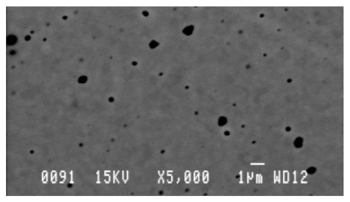
SEM image of the zirconia sample with pores in the surface (black). The alumina samples have very similar microstructure. Image courtesy of Lars Eklund, Swerea IVF.
The bulk scattering due to porosity in sintered highly-dense alumina can be characterized numerically using the scattering coefficient, µs, and the anisotropy factor, g. The former can be calculated from the measured collimated transmittance of a thin sample ensuring least-scattering regime (often called in-line transmittance, TC, in the ceramic area) using the Beer-Lambert law,
| (1) |
where TF is the Fresnel transmittance, and d is the thickness of the sample. A Mie calculation, with the assumption of log-normal distributed spherical pores, may provide a very close fit to the measured scattering coefficient. In our previous study we found that this agreement would not be achieved if mono-disperse pores are considered [7]. As a by-products of this fitting the anisotropy factor, the pore size distribution and porosity are then obtained. More details about the Mie calculation of the light scattering by pores in ceramic material can be found in [17].
In the presence of surface roughness the measured in-line transmittance may be reduced, and it will affect the fitting of the Mie calculation. The correction can be simply done by substituting TF in Eq. (1) by the product of TF and the loss of transmittance in the specular direction due to the roughness [18]. In this case Eq. (1) can be rewritten as
| (2) |
where σ is the root-mean-square (rms) roughness corresponding to a cutoff spatial wavelength of 250 µm [19], λ is the wavelength of incident light, and n is the refractive index of the material. The factor (1 + n2) is for the adjustment of the wavelength to the refractive index, i.e. the wavelength is λ/n inside the material.
This is a simple model by which we can evaluate the bulk scattering separately without being disturbed by the surface scattering. The obtained bulk scattering parameters are therefore more accurate and this will enhance the accuracy of our Monte Carlo simulation of OCT images.
3. Materials and methods
3.1 The alumina and zirconia ceramic samples
For the experimental work the sintered highly dense polycrystalline alumina and zirconia ceramic materials are provided by Swerea IVF [20]. The former has very high purity close to the theoretical limit while the latter contains 3 mole percent yttria. The wavelength dependent refractive index, n of alumina is calculated from [21]
| (3) |
The refractive index of 3 mole percent yttria-stabilized zirconia is calculated from [22]
| (4) |
The imaginary parts of the refractive indices of both materials are close to zero in the range λ = 0.5-4 μm, i.e. the absorption of the radiation can be neglected.
The samples studied by OCT imaging include two alumina flat sheets with the thickness of 450 μm, an alumina sheet containing several laser-milled channels with widths from tens to hundreds µm and depths of about 65 µm in the top surface, and a zirconia flat sheet with the thickness of 375 μm. For investigating the effects of surface roughness on OCT imaging, one of the alumina flat sheets is polished on both sides. The polishing of such thin ceramic layer is very difficult because a large force is needed to push the sample that is fragile. Polishing on thinner alumina sheets is therefore not attempted. As result the polished alumina sample has an rms roughness σ = 30 nm, while the un-polished alumina and zirconia samples have σ = 90 nm as measured with a cutoff spatial wavelength of 250 µm.
Two alumina and zirconia samples used for the spectrophotometry measurement had thickness of around 100 μm, i.e. which are sufficiently thin for measuring in-line transmittance. For OCT imaging we select the thickness of the flat sheets to be around 400 μm because this is a typical value for micro-manufactured multi-layered ceramic devices. Below this thickness some features are usually embedded, such as the micro channels. It is also worth mentioning that this thickness approaches and challenges the detection limit of OCT in these ceramic materials.
3.2 Optical testing methods
The in-line transmittance is obtained from spectrophotometry measurements in the wavelength region 0.5-4 µm where absorption is negligible. The surface roughnesses are measured using a Zygo NewView 7300 scanning white light interferometer [23]. The FORTRAN code of the Mie calculation used in this study was originally developed by Mishchenko et al. [24]. For OCT imaging of the ceramic samples two laboratory swept-source OCT systems operating at 1.3 and 1.7 μm central wavelength (Wellman laboratory) and a commercial spectral-domain OCT operating at 1.3 μm (Thorlabs Telesto) were used [9,25]. The specifications of the systems are given in Table 1.
Table 1. Specifications of the Swept-source OCT Systems.
| OCT systems | Telesto | Wellman laboratory | |||
|---|---|---|---|---|---|
| Centre Wavelength | 1325 nm | 1300 nm | 1670 nm | ||
|
|
|
||||
| Axial Scan Rate | 5.5 kHz * | 10 kHz | |||
| Sensitivity | 106 | 105 dB | 100 dB | ||
| Lateral Resolution | 15 µm | < 20 µm | |||
| Axial Resolution | < 8 µm (in air) | < 20 µm (in air) | |||
5.5 kHz for high-sensitivity mode, up to 91 kHz for high-speed mode.
3.3 Monte Carlo simulation
For the Monte Carlo simulation of the OCT images of the ceramic samples presented here we used the Monte Carlo code developed and tested in previous studies [26,27]. A dedicated geometric model involving various surface roughness parameters is employed. The input scattering parameters and detection conditions are based on the experimental results derived from spectrophotometry measurements and OCT setups specifications. In addition we take dispersion effects into account as a relatively large bandwidth is required for maintaining a short coherence length. This is done by a weighted summation of the images obtained at the central wavelength λ and neighboring wavelengths at the both sides of it, namely:
| (5) |
where Idisp is the obtained simulated OCT image with account of dispersion, Δλ is the bandwidth (FWHM) of the source, Iλ and Iλ ± Δλ/2 are the OCT images calculated for the central wavelength and the wavelengths λ ± Δλ/2, respectively. Our preliminary studies have shown that more accurate assessment of the dispersion including larger set of wavelength is excessive for the considered materials.
4. Experimental results
4.1 Scattering properties
The scattering coefficient and the anisotropy factor of the alumina and zirconia ceramic samples are shown in the figures below. The scattering coefficient obtained from Mie calculation fits very well with that calculated from the measured in-line transmittance which is compensated with surface scattering using Eq. (2). The signal-to-noise ratio of the transmittance measurements is extremely low at λ = 0.5 µm. This results in large uncertainty in the calculation of the scattering coefficients for both materials. Therefore, we skip this wavelength in fitting the data. The fitting of the pore size distributions and porosity is then obtained as listed in Table 2.
Table 2. Pore Size Distributions and Porosity of the Alumina and Zirconia Samples.
| Mean pore diameter | Standard deviation of pore size distribution | Porosity | |
|---|---|---|---|
| Alumina | 0.4 µm | 0.35 µm | ≈1% |
| Zirconia | 0.2 µm | 0.32 µm | ≈0.2% |
As can be seen in Fig. 2, the scattering is very strong in the visible region where the wavelength is comparable to the pore diameters, corresponding to the so-called Mie scattering regime. For the alumina sample the scattering coefficient decreases with increasing wavelength and approaches a very small value at 4 µm where absorption will start playing a role on the total light extinction [7]. For the zirconia sample, having smaller pore sizes and porosity, the scattering coefficient is lower than that of the alumina sample. From λ = 2 µm the scattering coefficient becomes very small and remains at this level for the longer wavelengths.
Fig. 2.
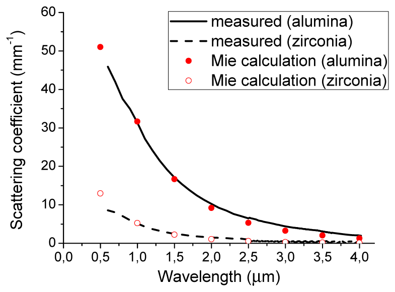
Spectra of the scattering coefficients of the alumina and zirconia ceramic samples. The lines represent the results calculated from the measured in-line transmittance, and the circles present the results obtained from Mie calculation.
The anisotropy factors of the alumina and zirconia samples obtained from the Mie calculations also show a descending trend with wavelengths (Fig. 3). The smaller the g-factor is, the more isotropic is the scattering by a single small pore, and the smaller is the ratio of the pore size to wavelength. The g-factor of the alumina sample containing larger pores is therefore higher compared to that of the zirconia sample in this wavelength region.
Fig. 3.
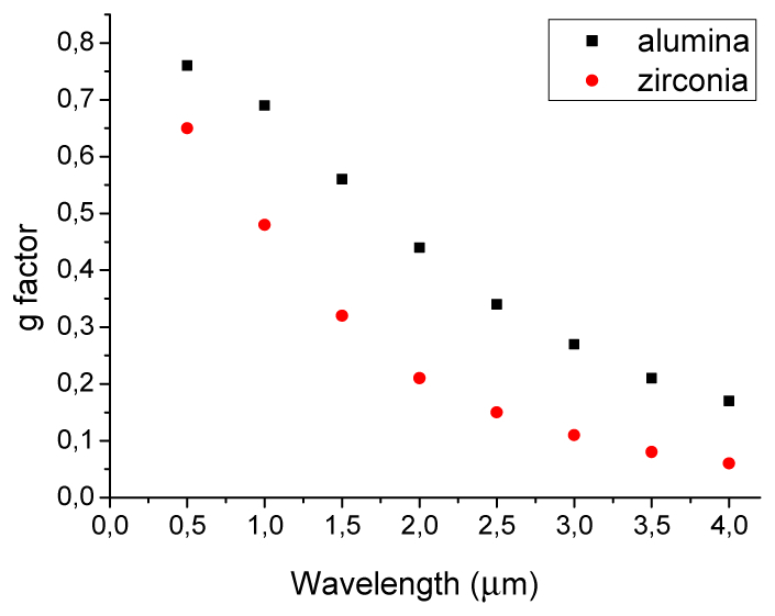
Derived anisotropy factors from Mie calculations of the alumina and zirconia ceramic samples.
4.2 OCT inspection
Experimental OCT images are obtained by the laboratory setups operating at 1.3 and 1.7 µm. The ceramic sample stack to be measured by OCT is built by covering the alumina sheet with laser-milled channels by the polished and un-polished flat alumina layers, respectively. The geometry of the sample stack and the imaging cross section is shown in Fig. 4.
Fig. 4.
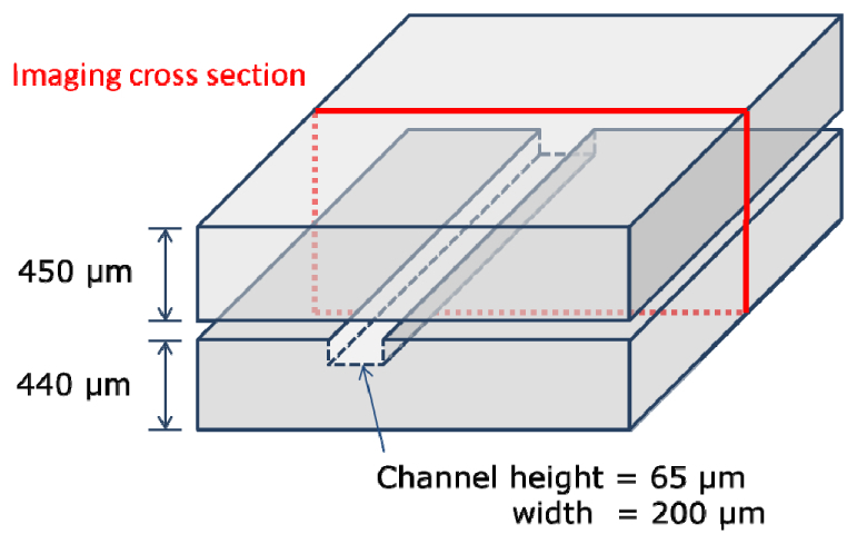
Geometric model of the ceramic sample stack. The imaging cross section is marked as the red frame. The callouts indicate the corresponding dimensions. The thickness of the top layer is 375 µm for the zirconia sample in the experiment.
The traceability of the thickness measurement of each layer and the dimensions of the micro-channel is highly important in quality control of micromanufacturing. As current non-destructive testing (NDT) technology cannot provide traceable measurements of sintered embedded features in ceramics with well-known measurement uncertainty and repeatability we had to use a ceramic stack of two non-bonded sample layers, so the thicknesses and the channels could be accurately measured using standard techniques. This however, may introduce an air gap between these two layers due to the waviness in the surfaces.
The cross-sectional OCT measurements of the alumina sample stack are shown in Fig. 5 as B-scan images obtained at 1.3 and 1.7 µm wavelengths respectively. The rear boundary of the polished 450 µm-thick alumina layer can be detected at 1.7 µm (B) but not at 1.3 µm (A). This result shows that the 1.7 µm OCT provides a larger probing depth compared to the 1.3 µm OCT, given that the systems configurations are quite similar. It has also been found that the 1.3 µm OCT has a limited probing depth around 300 µm in the same type of alumina material [28].
Fig. 5.
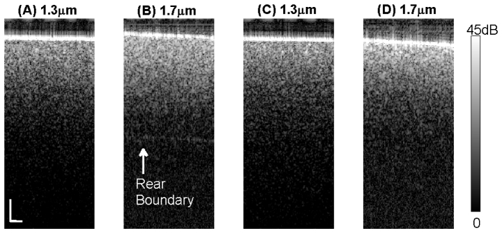
Cross-sectional B-scan OCT images of the alumina sample stack. A) λ = 1.3 µm, polished top layer; B) λ = 1.7 µm, polished top layer; C) λ = 1.3 µm, un-polished top layer; D) λ = 1.7 µm, un-polished top layer. The vertical and horizontal bars are 150 µm, where the former represents optical distance. The background noise is slightly higher for the 1.7 µm OCT system. The Wellman laboratory OCT systems are used.
Figure 5(c) and 5(d) represent the OCT measurements of the alumina stack with the 450 µm un-polished alumina flat sheet on top. In this case the 1.7 µm OCT measurement cannot detect the rear boundary due to the additional scattering by the rougher surface. Moreover, the laser-milled channel is not detected at all due to the strong bulk and roughness scattering. This is the major motivation for presenting the idea and an investigation on an optimal OCT wavelength for ceramics by using Monte Carlo simulation in the mid-IR region.
The image of the sample stack with the 375 µm zirconia top layer taken by the commercial OCT system operating at 1.3 µm center wavelength (shown in Fig. 6) presents a better detectability of the rear boundary compared to that of alumina as shown in Fig. 5(a) and 5(c). This is because our zirconia material is thinner, contains smaller pores and has lower porosity. The direct comparison with alumina samples is not performed here because of the unequal geometry of the zirconia sheet, but this will be done by simulation in which the geometric model for both materials is set the same.
Fig. 6.

Cross-sectional OCT image of the ceramic stack with the 375 µm-thick zirconia top layer as measured by the Thorlabs OCT system working at 1.3 µm. The horizontal bar is 200 µm and the vertical bar corresponding to optical distance of 150 µm.
5. Monte Carlo simulations of OCT images
The OCT images shown in Fig. 5 are used as references for the comparison with the Monte Carlo simulations that are based on the physical and optical parameters of both, the OCT systems and the samples. Particularly, quantitative agreement is achieved between the simulations and Fig. 5(b) and 5(d), where several criteria to be fulfilled will be discussed in section 5.2.
5.1 Geometric models and input parameters
The geometric model of the simulation is based on the experimental two-layer stack shown in Fig. 4, where a flat layer is placed atop the bottom layer with a rectangular channel in its upper surface. The two layers are separated by a thin air gap as observed in the experimental measurements. Figure 7 shows the geometry of the imaging cross section input to the Monte Carlo simulation code. The only difference between model I and II is that the rms roughness σ of the surfaces of the top layer is higher in model II, 90 nm for the unpolished case, compared to 30 nm for the polished model I case. The surfaces of the bottom layer have σ = 90 nm, and a higher roughness, σ = 140 nm, is used for the laser-milled surface in the channel. For convenience we will use S1, S2, S3, and S4 in the following context for presenting the corresponding surfaces in Fig. 7.
Fig. 7.

Schematic cross-sectional geometric models input to the Monte Carlo simulation program for simulating OCT images. The axes correspond to physical lengths. The models are applied to both alumina and zirconia samples for direct comparison of the simulation results. S1-S4 represents the four surfaces and σ the different rms roughness values.
The other important inputs are the optical parameters of the materials and the OCT setups. Table 3 lists the calculated refractive index n, the scattering coefficient µs, and the anisotropy factor g of the alumina and zirconia materials for the five wavelengths to be used in the simulation. As already mentioned, absorption is very small in the considered wavelength region and it is therefore set to zero.
Table 3. Optical Properties Input to the Monte Carlo Simulation Program.
| Alumina | Zirconia | ||||||
|---|---|---|---|---|---|---|---|
| λ (µm) | n | µs (mm−1) | g | n | µs (mm−1) | g | |
| 1.3 | 1.751 | 22.4 | 0.61 | 2.207 | 3.2 | 0.38 | |
| 1.7 | 1.744 | 14.4 | 0.54 | 2.198 | 2.0 | 0.27 | |
| 2 | 1.738 | 10.6 | 0.44 | 2.192 | 1 | 0.21 | |
| 3 | 1.712 | 4.6 | 0.27 | 2.169 | 0.9 | 0.11 | |
| 4 | 1.675 | 2.1 | 0.17 | 2.138 | 0.7 | 0.06 | |
The input OCT parameters are set to fit the experimental setup and are listed in Table 4. The effective detector radius and detection angle corresponds to the aperture stop and the numerical aperture (NA). More details about these parameters can be found in [27].
Table 4. OCT Parameters Input to the Monte Carlo Simulation Program.
| Pixel size | Lateral resolution | Axial coherence length | Effective detector radius |
Effective detection angle |
|---|---|---|---|---|
| 10 × 10 µm | 20 µm | 12 µm | 12 µm | 2 degree |
In addition, the number of the photons launched for each simulated A-scan is 50 million in order to provide enough statistics comparable to a sensitivity of 100 dB in the experiment.
5.2 Results
5.2.1 Comparisons of A-scans
Before a discussion on the simulated result we need to have a quantitative comparison between the experiment and the simulation. We consider that the quantitative agreement is achieved only if the following three criteria are fulfilled: (a) the rear boundary of the top layer is only detectable using the 1.7 µm OCT when the surface roughness is small (σ≈30 nm); (b) nothing from the bottom layer can be detected; and (c) the slope of the OCT signal attenuation is the same.
The average A-scans of the measured OCT image (at λ = 1.7 µm) of the polished and un-polished alumina samples (shown in Fig. 5) are compared with the average A-scans of the simulated images for λ = 1.7 µm, alumina, model I and II. As shown in Fig. 8, both simulations of the polished and un-polished model match the experimental results very well. The discrepancy of the signal levels of the first peaks (corresponding to the top surfaces S1) is mainly due to the reduced Fresnel reflection by the tilting of the samples in the experiment. It is important to note the small peak located at 785 µm which corresponds to the rear boundary of the polished top layer (S2) and can only be observed in Fig. 8(a).
Fig. 8.
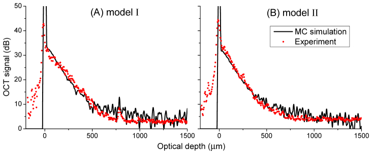
Quantitative comparison of the experimental and simulated OCT A-scans from alumina samples (model I and II). The averaged A-scans (over 50 A-lines) extracted from A) Fig. 5(b) and B) Fig. 5(d) are shown as red dots, and the simulated averaged A-scan for λ = 1.7 µm, alumina is shown as the black line. The simulated A-scans are truncated at a dynamic range of 50dB in this figure.
In Fig. 9 we can see that quantitative agreement is achieved between the measured and simulated average A-scans of the 375 µm zirconia sample. We have demonstrated that quantitative agreement is achieved between the experiment and the Monte Carlo simulation of OCT images of the ceramic materials without fitting of the optical parameters. Thus, the simulation is accurate enough for providing further analysis and predictions in this study.
Fig. 9.
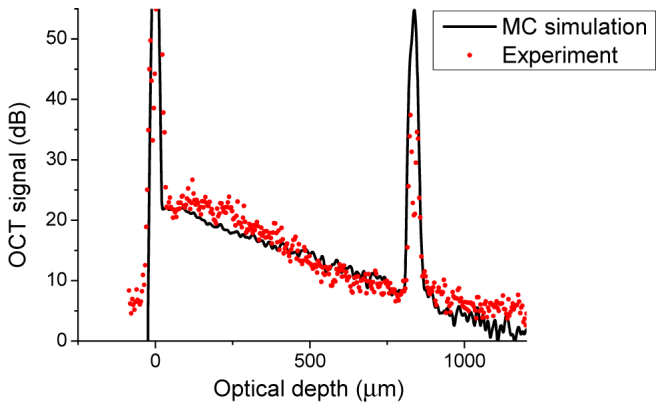
Quantitative comparison of the experimental and simulated OCT A-scans from zirconia sample. The averaged A-scan, extracted from Fig. 6, is shown as red circle and the simulated averaged A-scan is shown as black line.
5.2.2 Simulated OCT images for alumina
As mentioned before, surface roughness and porosity are the main causes of the scattering in highly-dense alumina and zirconia ceramics for the near infra-red wavelength region. The aim of this study is to explore whether OCT imaging benefit from the reduced surface and bulk scattering by increasing the wavelength. Figure 10 demonstrates the simulated images of model I (30 nm rms surface roughness) for alumina at five different wavelengths, where the dispersion effects are accounted for λ = 3 µm and 4 µm, and we will come back to this point later. It is obvious that the trend is an improved probing depth with increasing wavelength originating from the wavelength dependence of the optical properties of alumina, namely, µs and g. The intensity gradient of the 450 µm-thick top layer attenuates more quickly at λ = 1.3 µm than at 4 µm. i.e. the backscattering proportional to µs(1−g) is weaker, giving lower signal drop. The imaging contrast of the embedded boundaries is also considerably enhanced originating from weaker extinction of the probing beam.
Fig. 10.
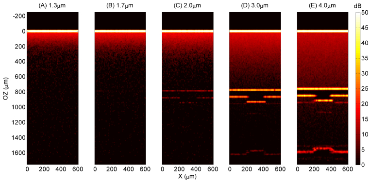
Simulated OCT images of alumina obtained by model I (30 nm rms surface roughness of the upper 450 µm-thick layer) for the five indicated wavelengths, where dispersion is accounted for λ = 3 µm and 4 µm. The vertical axis represents the optical distance as shown to the far left and the color-coded calculated intensity is given to the far right. The inverted channel signature at the bottom boundary is caused by shorter optical path through the air (black) in the channel.
Figure 10(a) and 10(b) should be compared with the measured OCT images Fig. 5(a) and 5(b). The simulated and measured images show that an OCT system operating at 1.3 µm cannot detect any embedded boundary at the bottom of the uppermost layer. At λ = 1.7 µm the rear boundary of the top layer (S2), located at the optical depth OZ≈785 µm, can be traced but it appears very weak and has a poor contrast, similar to the experimentally obtained image in Fig. 5(b). In Fig. 10(c)-10(e) we predict by our simulation the performance of an OCT systems operating at 2 µm, 3 µm and 4 µm. The upper surface of the bottom layer (S3) and the channel start to show up in Fig. 10(c), and turns clearer and clearer in Fig. 10(d) and 10(e) in which even the rear surface of the bottom layer (S4) can be observed.
In addition to the improved probing depth we also note a mirrored image of S3 just 90 µm (optical distance) beneath that surface. This is due to a double reflection between S2 and S3 when the probing depth is sufficiently large and the roughness of the embedded surface is small enough to keep surface scattering at a low level. At λ = 4 µm the transparency of alumina is higher and we observe the image artefacts of S2 and S3 as mirrored by the top surface S1 and appear at OZ≈1500 µm and OZ≈1680 µm. Because the thicknesses of the top layer and channel layer are quite close, the mirror image artefacts show up around the position of the real image of S4, which may disrupt the recognition of the latter.
Another phenomenon is the distorted image of the flat surface S4 as observed in Fig. 10(d) and 10(e). An inverted channel is shown in the image instead of a straight line because the probing radiation has travelled a shorter optical pathlength (air in the channel) to reach and return from this boundary at the channel region. The image distortion can easily be calculated as the optical paths difference, but it also shows how easily OCT images can be misinterpreted by the human visual perception.
In application to inspection of industrial ceramic materials [8], the surfaces of multiple layers in a ceramic device are of major interest to measure. Figure 11 demonstrates the simulated OCT images of model II for alumina at the five different wavelengths.
Fig. 11.
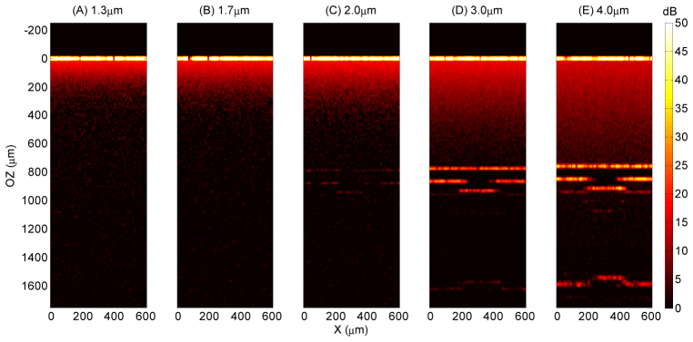
Simulated OCT images of alumina obtained by model II (90 nm rms roughness of the surfaces of the upper layer appearing at optical distances OZ = 0 and around 780 µm) for the five indicated wavelengths, where dispersion is accounted for λ = 3 µm and 4 µm. The vertical axis represents the optical distance as shown to the far left and the color-coded calculated intensity is given to the far right. The inverted channel signature at the bottom boundary is caused by shorter optical path through the air (black) in the channel.
In this case the two surfaces of the top layer have an rms roughness σ = 90 nm, corresponding to the un-polished alumina sample. We find that the embedded surfaces cannot be detected at all at λ = 1.3 µm and 1.7 µm. This agrees well with the measured images Fig. 5(c) and 5(d). Although the probing depth can be seen to be gradually improved with increasing wavelengths, the influence of the roughness of the top layer is obvious. The OCT signals of all embedded boundaries drop and the discontinuity of each boundary is more pronounced due to large-angle deflection at the surfaces. All these effects make the detections more difficult.
As we set the axial coherence length identical for the five indicated wavelengths, dispersion effects need to be accounted, particularly at λ = 3 µm and 4 µm for which the required bandwidth Δλ (FWHM) of the corresponding source is 0.3 µm and 0.6 µm, respectively. For the smaller wavelength the variation of the optical properties within corresponding bandwidth is small enough, so the dispersion effects can be neglected. As presented in Fig. 12 we directly compare the simulated OCT images of alumina obtained by both model I and II for λ = 4 µm, with and without account of dispersion. The dispersion effects are obvious as can be seen in Fig. 12(b) and 12(d), where the boundaries S3 and S4 appear more blurry and less bright compared to those in Fig. 12(a) and 12(c). This result, that the degradation of axial resolution and detection sensitivity can be caused by dispersion, agrees very well with the theory [13]. However, we have found that the dispersion effects are less pronounced for λ = 3 µm with Δλ = 0.3 µm, and can also be reduced effectively for λ = 4 µm by downgrading the axial coherence length to 20 µm that corresponds to Δλ = 0.3 µm, or by other compensation methods [13].
Fig. 12.
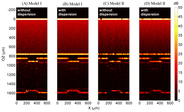
Comparison of the simulated OCT images of alumina obtained by both model I and II for λ = 4 µm, with and without account of dispersion. The vertical axis represents the optical distance as shown to the far left and the color-coded calculated intensity is given to the far right.
5.2.3. Simulated OCT images for zirconia
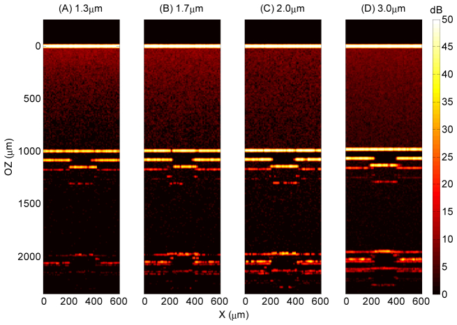
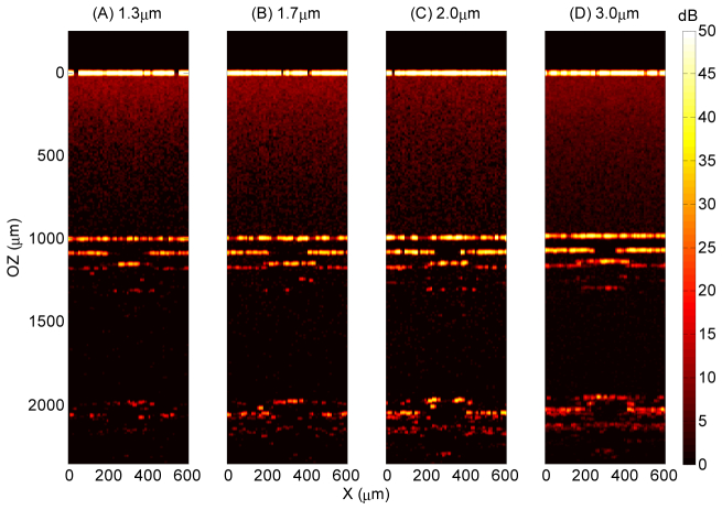
As a final demonstration of the predicted performance of OCT imaging at mid-IR wavelengths we present in Fig. 13 and Fig. 14 the simulated results for zirconia. The same geometric models I and II (Fig. 7) are applied for the zirconia ceramic material in order to have a direct comparison with the alumina material. It is therefore not directly comparable with the experimental data of Fig. 6 which is obtained from a 375 µm layer. In Fig. 13 we demonstrate the simulated OCT images of model I for zirconia at the four wavelengths, 1.3 µm, 1.7 µm, 2 µm and 3 µm. The dispersion effects are accounted for λ = 3 µm, which makes the embedded boundaries more blurry and reduces the signal levels similar to the alumina case. The probing depth is improved with increasing wavelength up to λ = 2 µm. But then, it comes to a limit as the difference is quite small between Fig. 13(c) and 13(d). From the optical properties (Table 3) we can predict that the simulation at 4 µm would not improve the probing depth further for this type of zirconia.
Fig. 13.
Simulated OCT images of the smoother surface model I for zirconia at four different wavelengths. Dispersion is accounted for λ = 3 µm. The vertical axis represents the optical distance as shown to the far left and the color-coded calculated intensity is given to the far right.
Fig. 14.
The same simulation as in Fig. 13 but now using model II, with a roughness of 90 nm rms of the surfaces of the upper layer appearing at optical distances OZ = 0 and around 1000 µm. Dispersion is accounted for λ = 3 µm.
Again, we observe the mirrored images of S3 just 90 µm beneath it due to double or even triple reflection, as well as the mirrored images of S2 and S3 at OZ≈1950 µm and OZ≈2130 µm. We can also observe the distorted image (inverted channel profile) of S4 caused by the shorter optical path through the air filled embedded channel. Moreover, the scattering in zirconia is much weaker compared to that in alumina. Thus, the mirrored image artefacts become more pronounced, and interfere with the image of S4, which makes the image recognition and therefore the boundary detection very difficult.
By comparing Fig. 10 and Fig. 13 it is obvious that the embedded boundaries are more easily found in the zirconia material. The differences are particularly large at λ = 1.3 µm, 1.7 µm and 2 µm, where the scattering coefficients of the alumina sample are much larger than for the zirconia sample. Also, it is obvious that the OCT signal slope for the zirconia material is smaller, particularly for longer wavelengths due to smaller corresponding scattering coefficient values.
The simulated OCT images of model II for zirconia at the same four wavelengths are shown in Fig. 14. The influence of surface roughness is apparent as the images of the embedded boundaries become fuzzy and fragmented. By comparing Fig. 11(d) with Fig. 14(b), corresponding to similar µs and g values, but a considerably higher refractive index for zirconia, we can see that the influence of surface roughness is enhanced when the refractive index is higher. In addition, it becomes difficult to detect the channel which has a surface roughness σ = 140 nm as shown in Fig. 14. This means that the detection of embedded boundaries does not only depend on the probing depth, limited by the bulk scattering, but also depends on the roughnesses of the surfaces through which the radiation is transmitted and the targeting surfaces from which the radiation is reflected.
6. Conclusion
In this study we experimentally analyze the effect of surface and bulk scattering on the probing depth of near to mid-IR optical coherence tomography (OCT) in ceramic materials. Two materials, alumina and zirconia, were measured at 1.3 and 1.7 µm wavelengths. Spectrophotometric measurements revealed the scattering coefficients and g-factors in the wavelength range from visible to 4 µm. Based on these results, experimentally measured surface roughness, and optical parameters for the OCT-setup Monte Carlo simulations of the OCT images over an extended wavelength range with account of dispersion were performed. Without any fitting and adjustment of the measured dimensions, the determined optical properties of the samples and physical parameters of the OCT optics a quantitative agreement was achieved with the measured OCT images at 1.3 and 1.7 µm. Comparisons made at different surface roughnesses and wavelengths reveal the physical mechanisms behind the quality of OCT images and provide an understanding of the optimal imaging conditions.
A major problem of OCT inspection of multilayer ceramic structures is its limited probing depth when the material is highly scattering. The optimal center wavelength is found to be 4 µm for the alumina samples and 2 µm for the zirconia samples. Suitable sources, IR bandpass filters, and detectors have been developed for these wavelength regions making future implementation of such OCT systems to be quite realistic. However, the presence of rough surfaces (σ~0.1 µm) will still make the images of embedded boundaries quite fuzzy. In contrast to biomedical applications of OCT, where the primary objective is to visualize internal structures, for the industrial applications high quality imaging of embedded boundaries of layer surfaces, delaminations, machined structures and other interfaces between different materials is required. The reason is the target of quantified dimensional metrology of industrial ceramic samples.
Then, it is not only the probing depth that determines if an embedded boundary can be detected or not. As shown in our analysis the roughnesses of all surfaces that the OCT rays interact with play an important role. There are also some other factors affecting the accuracy of OCT detection in ceramic materials. Although the axial measurement of OCT is verified through the simulations in our case, one cannot expect such a good correlation if the refractive indices of the materials are inaccurate or non-uniform. Internal reflections at close lying boundaries may create artefacts and disturb the observed structure, and air pockets altering the phase of the transmitted/back reflected rays may appear as inverted structures in the deeper lying interfaces. Dispersion effects will cause the image of the embedded boundary to be a bit blurred and reduce the signal level, in particular at large depths. All these artefacts will cause problems for automated image recognition by computers, and for the non-experienced observer the images may easily be misinterpreted.
Furthermore, some problems need to be addressed for the development of industrial OCT:
The central probing wavelengths of modern commercial OCT setups are aimed for the optical transparency window in biotissues, while for industrial applications different wavelengths can be more efficient as we have shown.
More efforts are needed for developing the proper components, such as light sources and detectors working in the mid-IR region.
Measurement errors of critical dimensions are more difficult to be defined in the lateral directions than the axial direction because of the light scattering from the edges and other optical phenomena. This information is missing in the literature.
Careful calibration is necessary if OCT will be used as a metrology tool. That requires sufficient knowledge of measurement uncertainty for the dedicated measurement. However, we are lacking of calibration standards with well-known embedded features. Also some standard image processing methods are required for OCT images.
Finally we conclude that the successful introduction of our dedicated Monte Carlo OCT simulation, taking into account both surface and bulk scattering, open up for investigations of other materials with different structures and at different wavelengths.
Acknowledgment
This work was partly supported by the joint European project Multilayer ( FP7-NMP4-2007-214122) and National Institute of Health ( P41EB015903). The authors would like to acknowledge Dr. Johanna Stiernstedt at Swerea IVF and Dr. Petko Petkov at Cardiff University for preparing the samples, Prof. Arne Roos at Uppsala University for supporting the spectrophotometry measurement, and Dr. Michael Leitner, Christian Lührs and Laura Hinkel supporting the Telesto OCT test at Thorlabs GmbH (Lübeck).
References and Links
- 1.Drexler W., Fujimoto J. G., eds., Optical Coherence Tomography Technology and Applications, (Springer, 2008). [Google Scholar]
- 2.Stifter D., “Beyond biomedicine: a review of alternative applications and developments for optical coherence tomography,” Appl. Phys. B 88(3), 337–357 (2007). 10.1007/s00340-007-2743-2 [DOI] [Google Scholar]
- 3.First international symposium on optical coherence tomography for non-destructive testing, (Linz, Austria, 2013), http://www.oct4ndt.at [Google Scholar]
- 4.Duncan M. D., Bashkansky M., Reintjes J., “Subsurface defect detection in materials using optical coherence tomography,” Opt. Express 2(13), 540–545 (1998). 10.1364/OE.2.000540 [DOI] [PubMed] [Google Scholar]
- 5.Sinescu C., Negrutiu M. L., Todea C., Balabuc C., Filip L., Rominu R., Bradu A., Hughes M., Podoleanu A. G., “Quality assessment of dental treatments using en-face optical coherence tomography,” J. Biomed. Opt. 13(5), 054065 (2008). 10.1117/1.2992593 [DOI] [PubMed] [Google Scholar]
- 6.Ellingson W. A., Visher R. J., Lipanovich R. S., “Optical NDE techniques for ceramic thermal barrier coatings,” Mater. Eval. 1, 1–17 (2006). [Google Scholar]
- 7.Su R., Kirillin M., Ekberg P., Roos A., Sergeeva E., Mattsson L., “Optical coherence tomography for quality assessment of embedded microchannels in alumina ceramic,” Opt. Express 20(4), 4603–4618 (2012). 10.1364/OE.20.004603 [DOI] [PubMed] [Google Scholar]
- 8.R. Su and L. Mattsson, “Evaluation of optical inspection methods for non-destructive assessment of embedded microstructures and defects in ceramic materials,” in Proceedings of the 9th International Conference on Multi-Material Micro Manufacture, Humbert Noll, Nadja Adamovic, and Stefan Dimov, eds. (Research Publishing, 2012), pp. 109–112. [Google Scholar]
- 9.Sharma U., Chang E. W., Yun S. H., “Long-wavelength optical coherence tomography at 1.7 microm for enhanced imaging depth,” Opt. Express 16(24), 19712–19723 (2008). 10.1364/OE.16.019712 [DOI] [PMC free article] [PubMed] [Google Scholar]
- 10.Cheung C. S., Tokurakawa M., Daniel J. M. O., Clarkson W. A., Liang H., “Long wavelength optical coherence tomography for painted objects,” Proc. SPIE 8790, 87900J (2013). 10.1117/12.2021700 [DOI] [Google Scholar]
- 11.Moselund P. M., Petersen C., Dupont S., Agger C., Bang O., Keiding S. R., “Supercontinuum: broad as a lamp, bright as a laser, now in the mid-infrared,” Proc. SPIE 8381, 83811A (2012). 10.1117/12.920094 [DOI] [Google Scholar]
- 12.Type II Super Lattice detector, IRnova AB, http://www.ir-nova.se/t2sl
- 13.Fercher A. F., Hitzenberger C. K., Sticker M., Zawadzki R., Karamata B., Lasser T., “Dispersion compensation for optical coherence tomography depth-scan signals by a numerical technique,” Opt. Commun. 204(1-6), 67–74 (2002). 10.1016/S0030-4018(02)01137-9 [DOI] [Google Scholar]
- 14.Serrels K. A., Renner M. K., Reid D. T., “Optical coherence tomography for non-destructive investigation of silicon integrated-circuits,” Microelectron. Eng. 87(9), 1785–1791 (2010). 10.1016/j.mee.2009.10.011 [DOI] [Google Scholar]
- 15.Gerhardt R., ed., Properties and Applications of Silicon Carbide, (InTech, 2011). [Google Scholar]
- 16.Stuer M., Bowen P., Cantoni M., Pecharroman C., Zhao Z., “Nanopore Characterization and Optical Modeling of Transparent Polycrystalline Alumina,” Adv. Funct. Mater. 22(11), 2303–2309 (2012). 10.1002/adfm.201200123 [DOI] [Google Scholar]
- 17.Peelen J. G. J., Metselaar R., “Light scattering by pores in polycrystalline materials: Transmission properties of alumina,” J. Appl. Phys. 45(1), 216–220 (1974). 10.1063/1.1662961 [DOI] [Google Scholar]
- 18.Caron J., Lafait J., Andraud C., “Scalar Kirchhoff's model for light scattering from dielectric random rough surfaces,” Opt. Commun. 207(1-6), 17–28 (2002). 10.1016/S0030-4018(02)01415-3 [DOI] [Google Scholar]
- 19.Bennett J. M., Mattsson L., Introduction to Surface Roughness and Scattering, (Optical Society of America;, June1999). [Google Scholar]
- 20.Swerea I. V. F., Mölndal (head office), Sweden, http://www.swerea.se/sv/ivf/
- 21.Malitson I. H., “Refraction and dispersion of synthetic sapphire,” J. Opt. Soc. Am. 52(12), 1377–1379 (1962). 10.1364/JOSA.52.001377 [DOI] [Google Scholar]
- 22.Wood D. L., Nassau K., Kometani T. Y., “Refractive index of Y2O3 stabilized cubic zirconia: variation with composition and wavelength,” Appl. Opt. 29(16), 2485–2488 (1990). 10.1364/AO.29.002485 [DOI] [PubMed] [Google Scholar]
- 23.Zygo NewView7300 3D optical surface profiler, http://www.zygo.com/?/met/profilers/newview7000/
- 24.Mishchenko M. I., Travis L. D., Lacis A. A., Scattering, Absorption, and Emission of Light by Small Particles, (Cambridge University Press, 2002). [Google Scholar]
- 25.O. C. T. Thorlabs Telesto, System, http://www.thorlabs.de/newgrouppage9.cfm?objectgroup_id=5274
- 26.Kirillin M., Alarousu E., Fabritius T., Myllylä R., Priezzhev A. V., “Visualization of paper structure by optical coherence tomography: Monte Carlo simulations and experimental study,” J. Eur. Opt. Soc.- Rapid Publ. 2, 07031 (2007). 10.2971/jeos.2007.07031 [DOI] [Google Scholar]
- 27.M. Kirillin, “Optical coherence tomography of strongly scattering media,” Doctoral thesis, Faculty of Technology, University of Oulu (2008). [Google Scholar]
- 28.R. Su, E. W. Chang, P. Ekberg, L. Mattsson, and S. H. Yun, “Enhancement of probing depth and measurement accuracy of optical coherence tomography for metrology of multi-layered ceramics,” presented at the First International Symposium on Optical Coherence Tomography for Non-Destructive Testing, Linz, Austria, pp. 71–73, (2013). [Google Scholar]


