Abstract
Plasmonic materials (PMs), featuring large static or dynamic tunability, have significant impact on the optical properties due to their potential for applications in transformation optics, telecommunications, energy, and biomedical areas. Among PMs, the carrier concentration and mobility are two tunable parameters, which control the plasma frequency of a metal. Here, we report on large static and dynamic tunability in wavelengths up to 640 nm in Al-doped ZnO based transparent conducting degenerate semiconductors by controlling both thickness and applied voltages. This extreme tunability is ascribed to an increase in carrier concentration with increasing thickness as well as voltage-induced thermal effects that eventually diminish the carrier concentration and mobility due to complex chemical transformations in the multilayer growth process. These observations could pave the way for optical manipulation of this class of materials for potential transformative applications.
The resonant frequency of plasmonic materials (PMs) can be tuned over a range1 by controlling the dielectric medium. This can produce new functional devices in which the optical response of can be engineered by manipulating designs and composition of currently studied metamaterials, where their unique optical properties are not seen in individual components2,3,4,5. The tuning of the resonant frequency in many PMs is achieved by carrier injection in semiconductors6, mechanical reorientation in microelectromechanical systems7, varying the dielectric environment8, and many other emerging phenomena. The recent report7 on a tunability of compliant metamaterials using high-strain mechanical deformation between the resonant elements in coupled resonators has drawn tremendous interest and shown a pathway for imminent applications. However, although the expensive manufacturing of complex large-volume and low-loss tunable PMs is still a formidable challenge in itself9, and may easily expand in new inexpensive directions to find applications if their tunability is either controlled by applying an electric field or varying the thickness of the materials. The onset of interband transition is 3.9 eV for Ag and 2.3 eV for Au, which is in the ultraviolet or green light, far way from the near infrared (NIR) which is the interest of materials being developed in this work.
The Fermi level (Ef), for some of the transparent conducting oxides (TCOs) known as degenerate semiconductors, is found within the conduction band (CB) or above the conduction band (Ec), as is found in a metal. For example, such is the case when the wide bandgap semiconductor ZnO is doped with either Ga or Al. These doped semiconductors demonstrate properties that are more metal than semiconductor-like with the resistivity, (ρ) being proportional to the temperature, (T). Doped (Ga or Al) ZnO based TCOs have shown the above electrical dependence and generic n-type behavior with high carrier concentrations10,11,12. This class of semiconductor materials demonstrates remarkable properties of low-loss PMs13,14,15,16,17 because semiconductors do not have bound-state absorption transitions in their band-gaps, and their surface plasmon polariton losses can be even smaller, in the NIR region than those with conventional plasmonic materials at corresponding visible wavelengths18. However, no significant tuning of the resonant frequency in this class of PMs16,19,20,21 has been achieved by varying different conditions, such as growth, doping concentration, etc. We demonstrate that the crossover wavelength (λc) can be widely tuned by varying the thickness of the layers, as well as by dynamically controlling the electric field on the surface of the films in this degenerate semiconductor.
Results
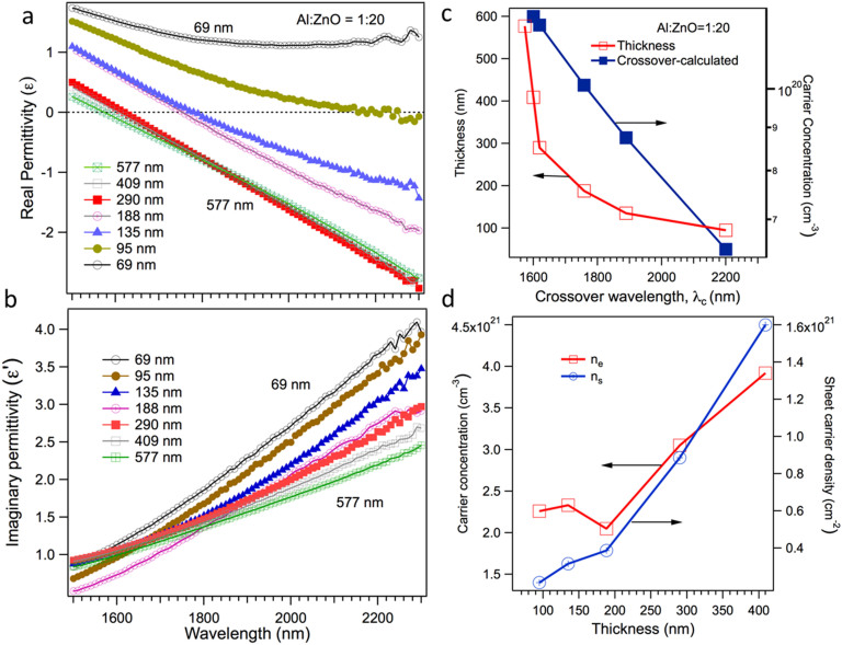
The Al-doped ZnO (AZO) thin films with varying thickness and multilayers comprising of different Al:Zn composition ratios were grown via alternate deposition of diethyl zinc (DEZ, Zn(C2H5)2), H2O and trimethylaluminum (TMA, Al(CH3)3) through atomic layer deposition (ALD) cycles22 (see supplementary information). ALD is used to attain conformal and pinhole-free films with a high degree of thickness control. The sequential exposure of reactants used in ALD adjusts the composition of multicomponent materials by changing the number of cycles used for each precursor materials (See schematics in Supplementary Fig. 1a). Variable angle spectroscopic ellipsometry (VASE) (see supplementary information) was used to measure the λc from positive to negative permittivity using the Drude-Lorentz model. Fig. 1a demonstrates the crossover of the real permittivity from positive to negative as the thickness of AZO films is varied from 69 to 577 nm. The corresponding imaginary permittivity (loss) is illustrated in Fig. 1b. The thickness dependence of λc is found to fall exponentially as the thickness of the films increases (Fig. 1c). While tunability of a PM is very desirable for device applications, tuning by manipulating the thickness could prove to be of particular importance for the fabrication of real devices. We found that the λc is significantly tunable with a range of 640 nm in the NIR region by simply changing the thickness of AZO films. While this large range of tunability is observed in the NIR range, the loss is significantly diminished as the thickness increases (Fig. 1b) due to higher conductivity in the thicker films. Moreover, the dispersion in the imaginary part of the permittivity is significantly less over the measured range.
Figure 1. Room temperature permittivity and carrier concentrations.
Wavelength dependence of the (a) real and (b) imaginary permittivity of Al:ZnO (1:20 ratio) films containing low (69 nm) to higher (577 nm) thickness. (c) Thickness dependence of crossover wavelength, λc, and calculated carrier concentration using the Drude-Lorentz model. (d) Dependence of measured carrier concentration (ne) and sheet carrier density (ns) of AZO films.
If we consider the plasma frequency of the film (ωp), which is defined by equation (1):
 |
and is related to the real part of the permittivity by the following equation (2):
 |
where ne is the carrier concentration, m0 is the effective mass,  is the permittivity due to interband transitions, and
  and e2 are the free-space permittivity and electron charge, respectively. In eq. (2) Γ is the total damping rate. The plasma frequency is directly proportional to the carrier concentration. It is also noted that the real permittivity should be negative for plasmonic materials. Fig. 1c shows the AZO film thickness and the corresponding calculated carrier concentration for the corresponding λc, while Fig. 1d shows the experimental carrier concentration, and sheet carrier density, ns with increasing thickness of the AZO films. The sheet carrier density was calculated from the Hall voltage. The trend of λc dependence on thickness can be related to the enhanced carrier concentration and sheet carrier density of the films, which validates the plasma frequency relation with carrier concentration in Eq. (1). Although the carrier concentration in Fig. 1c and d is slightly different, the discrepancy is due to the two separate techniques, such as carrier concentration calculated numerically using eq. (1) and λc for Fig. 1c and experimentally using Hall configuration for Fig. 1d. There is a large change in the resistivity going from as high as 1.19 × 10⁻³ Ω-cm for the 69 nm film down to as low as 7.9 × 10⁻⁴ Ω-cm for the 577 nm thick film. The metal-like behavior is noted for films with higher thickness (see supplementary information), which is basically due to Al donor electrons filling up the lower levels in the conduction band as seen in degenerate semiconductors. The columbic interactions between the positively charged metal ions are minimized in the ALD process23,24,25 by keeping the Al dopants as far apart as possible, which makes this process unique for controlling the carrier concentration. As we increase the number of macrocycles, the projected surface area is expected to increase26. This provides an enormous opportunity for passively tuning the PM devices during the ALD fabrication process by spatially varying the thickness, and hence the carrier density.
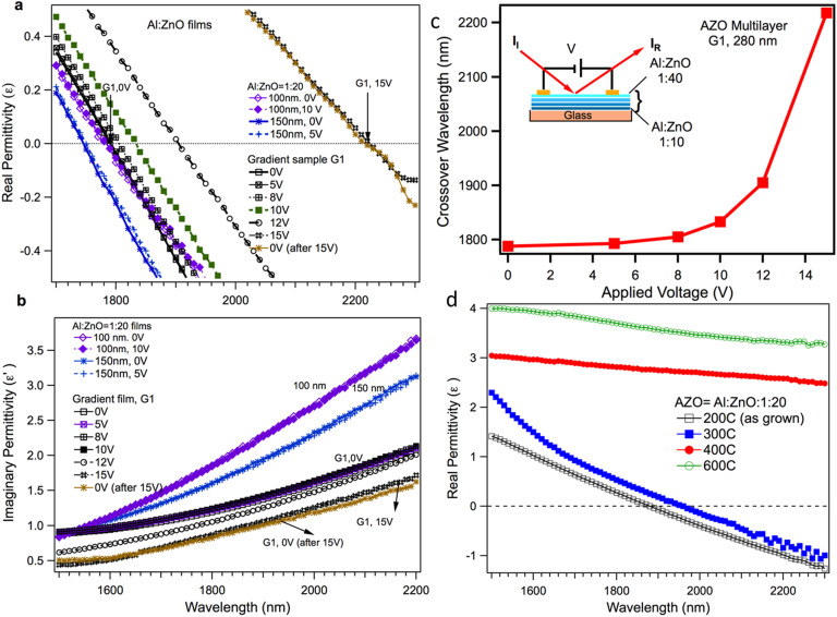
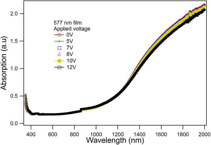
Figure 2a and b show the wavelength dependence of the real and imaginary permittivity with applied voltage, respectively, for the gradient sample, G1, in which the electron concentration is varied from bottom to top (Fig. 2c inset (See Supplementary Fig. 1b and c). The wavelength dependence of the real and imaginary permittivity with applied voltages are also shown for two sample thicknesses, 100 and 150 nm with Al:Zn = 1:20. The electric field controlled permittivity is an excellent method to dynamically control the plasmonic properties of AZO films. The λc of a specially designed multilayer AZO thin film (G1 gradient sample) in which the Al-content was varied along the thickness of the film (See Supplementary Fig. 1b and c) can be tuned up to 450 nm by simply applying a voltage on the sample as shown in Fig. 2c, thus demonstrating an electric field controllable plasmonic metamaterial for potential device applications with reasonably low loss at higher applied voltages (Fig. 2b). However, a contrasting effect is that λc does not show reversible behavior beyond the applied voltage of 12 V. Since these measurements combine both incident light and applied electric field, this observed effect may be related due to electro-absorption in a material, a phenomenon called the Franz-Keldysh effect27,28, that occurs in low-dimensional systems, such as quantum wells, quantum wires, and quantum dots due to quantum confinement effects29,30. In order to verify the Franz-Keldysh effect (see supplementary information) in these AZO samples, electro-absorption experiments were performed on the 577 nm thick films with applied voltages up to 12 V over the 300 to 2000 nm wavelength range for the incident light. No significant difference in electro-absorption characteristics was observed (Fig. 5 and supplementary information) in our experiments, which implies that the Franz-Keldysh effect has no significant influence on our AZO films.
Figure 2. Room temperature permittivity and carrier concentrations.
Wavelength dependence of the (a) real and (b) imaginary permittivity of Al:ZnO (1:20 ratio) films (100 and 150 nm) and gradient film, G1 (280 nm) at various applied voltages. Results are also shown for no applied voltage after the 15 V measurements, which exhibit irreversibility. (c) Applied voltage dependence of crossover wavelength, λc for the multilayer G1 film, where the Al:ZnO ratio varies from 1:10 to 1:40 (Supplementary Fig. 1). (d) Wavelength dependence of the real permittivity of 150 nm thick Al:ZnO (1:20 ratio) films annealed at various temperatures after growing at 200°C.
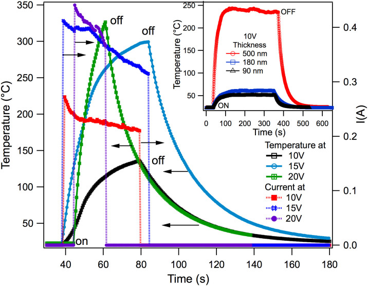
Figure 3. Thermal effects due to applied voltages.
The heat is generated due to applied voltages, and both on and off conditions are shown. The current (dotted lines) sharply rises with the applied voltages when switched on and suddenly falls off to zero when switched off. The samples cool down exponentially after the voltage is turned off. The inset shows the rise and fall of temperature with time for various film thicknesses for both on and off voltage cases.
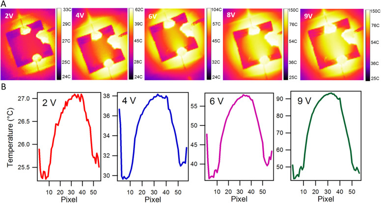
Figure 4. Thermal imaging of the film during application of voltages.
(A) The thermal imaging of the heat generated due to applied voltages using an infrared camera (320×240 pixel resolution) over a 1 cm2 area of the AZO film. (B) The temperature profile across the top left to bottom right diagonal of the rectangular sample at different applied voltages up to 9 V.
Figure 5. Optical absorption as a function of wavelength at various applied voltages for the 577 nm thick AZO (Al:Zn = 1:20) film.
In order to explore the reasons for this dynamic voltage induced tuning, some of the samples were annealed at various temperatures. The λc changed from 1878 to 1963 nm for the 150 nm thick as-grown films annealed at 300°C (Fig. 2d). However, for annealing temperature greater than 400°C, no trend of the real permittivity crossover was seen as is clearly shown in Fig. 2d, providing evidence that the number of free charge carriers has diminished31 according to Eq. (1) for films annealed at temperatures higher than 300°C. The above consequence provides a clear sign that the films are undergoing morphological changes, which impact the carrier concentration in the films.
In order to further investigate the reasons for dynamic electrical tunability, we performed a series of time-dependent electro-thermal experiments. While a specific voltage was applied onto the sample surface using deposited metal electrode pads, the temperature and current developed between the contacts were monitored over time as shown in Fig. 3 from 10 to 20 V for AZO films with thickness of 577 nm. Interestingly, a temperature rise to 325°C can be reached as the voltage increases to 20 V, similarly to 140 and 300°C for 10 and 15 V, respectively. The current follows a similar trend as the temperature, except that it falls off sharply as the voltage supply is ceased. Additionally, the temperature rise time is much faster for higher voltages than for lower ones. The ellipsometry measurements were performed by applying voltage on the samples for a duration of 8 to 10 h. This causes a Joule heating effect, which we have evidenced from precise thermal conductivity and electrical property measurements of the AZO films. The Joule heating effect is supported by the observed metallic behavior in temperature dependent electrical transport of these films (See Supplementary Fig. 2b and c). Thermal conductivity of AZO films was measured by the time-domain thermoreflectance (TDTR) technique32 (Supplementary Fig. 3), and the thermal conductivity was found with moderate value for the AZO films. For example, the room-temperature thermal conductivity for an AZO sample with thicknesses of 290 nm is 4.264 ± 0.11 W/m/K, and for the gradient sample (287 nm thick) it is 5.65 ± 0.38 W/m/K. TDTR measurements were performed at higher temperatures. The thermal conductivites are relatively constant from room temperature to 373K (supplementary information under thermal conductivity). This is explained in the frame-work of better metallic behavior observed in these samples (Supplementary Fig. 2), especially in thicker films. We also noticed higher heat generation due to Joule heating in thicker films (inset of Fig. 3). The moderate thermal conductivity in AZO films facilitates heat transport along the film, which causes the temperature to rise above 300°C at higher applied voltages. Prolonged applications at higher voltages raise the temperature to a level where the films get annealed, thus diminish the carriers.
The temperature distribution was recorded with an infrared camera over a 1 cm2 area of the AZO film. The gradual rise of the temperature is imaged and their corresponding temperature profiles are shown in Fig. 4 A, and B, respectively. These observations confirm that λc varies with the applied voltages, which produce thermal effects over the entire films, especially between the contact pads. It is noted that all the areas on the glass substrate except the square region (1 cm2) containing AZO film shown in Fig. 4A is etched out. Hence the heat dissipates from the film to the substrate underneath and the surrounding area. These results indicate that the voltage induced thermal effect is associated with the unique layer-by-layer structure of the films.
Recent cross-sectional microscopic studies revealed that ALD-grown AZO films are formed by a unique layer-by-layer structure, which is better explained as a nanolaminate structure, of a ZnO matrix and Al2O3 dopant layers25,33, where free electrons are provided to the ZnO matrix by the Al2O3 dopant layers. Due to the increased temperature, at the higher applied voltages, the local Al2O3 dopant layers form AlOx islands that cause interface scattering. This scattering reduces the mobility at the grain boundaries and decreases the carrier concentration, which is similar to the effects of annealing seen in ALD-grown AZO films31. Consequently, the decrease in carrier concentration shifts λc to a higher wavelength region, and finally the dielectric permittivity becomes positive due to a loss of carriers responsible for metallic behavior. The reversible tunability up to 12 V of applied voltage corroborates the fact that the thermo-morphological transformation is limited as shown in Fig. 2d for thermally annealed ALD-grown AZO films. However, above 12 V significant chemical and morphological transformation occurs due to nanolaminate structures forming AlOx-based electron trapping centers as well as severe interface scattering. Due to the wide tunability of λc, there is enough scope for these ALD-grown AZO films for telecommunication applications in the NIR region by fabricating suitable waveguides. The present experimental results clearly demonstrate the passive and dynamic fine tunability of AZO films due to the interplay of carriers and electro-thermal properties forming a transparent heater. The Joule heating (P = I2R, where I is current, and R is resistance) due to applied voltage gets saturated after a few seconds and dissipates after switching off the voltage. As the applied voltage is proportional to the current that develops, a larger heating effect is observed at higher applied voltages. At the same time, thicker films produce a much larger heating effect compared to thinner films due to higher carriers. This is due to generation of larger currents in thicker films as the progressive increase of current is seen with the increase of voltages as well as the thickness of the films. Further analysis should provide more insight into the details of the mechanism behind these novel findings.
Methods
Fabrication of Al doped ZnO
The Al-doped ZnO (AZO) samples were prepared using a Cambridge Nanotech Savannah 100 atomic layer deposition (ALD) system. The base pressure of the ALD system was 5.2 × 10⁻³ Torr and increased to 1.7 × 10⁻¹ Torr with ultra-high purity N2 inert carrier gas flowing through at 20 SCCM. The AZO film is grown by alternating between 15 ms pulses of diethylzinc (DEZ, Zn(C2H5)2) and H2O, and with periodic 15 ms pulses of Trimethylaluminum ((TMA), Al(CH3)3) as the aluminum dopant. Ultra- high purity continuously flowing N2 purges the chamber in between precursor pulses. The purge time was 5 seconds. The substrate temperature was set to a desired substrate temperature. In our study, we varied the thickness of the AZO films by increasing the number of Zn:Al = 20:1 macrocycles. The structural and sequence arrangements are schematically illustrated (See schematics in Supplementary Fig. 1A).
The gradient film, G1, was grown by systematically varying the macrolayers (ML) from 60 to 15 ML as we fix Al = 1 and vary the ratio for Zn = 10, 20, 30 and 40, as schematically shown in Supplementary Fig. 1B. The number of total macrocycles was 2400 giving a thickness of approximately 280 nm. (See schematics in Supplementary Information Fig. 1B).The TOF-SIMS measurements confirm that the gradient sample contains less Al as the ratio changes from A:Zn = 1:10 to 1:40 (See Supplementary Information Fig. 1C).
Electro-absorption
The phenomenon of electric field induced change in absorption (electro-absorption), named the Franz-Keldysh effect27,28, may be able to be experimentally seen in these AZO samples. If one considers the situation that an optical beam with frequency (ω) and a DC field are applied to the AZO sample, the total electric field is given by
 |
where E0 and E1 are the amplitudes of the DC and optical fields, respectively.
The polarization of the medium is given by
 |
Substituting equation (3) into (4), we may obtain the polarization that determines the optical properties of the medium at frequency ω
 |
Here only DC field related terms are given and the terms involving only the optical field are neglected since the light intensity was weak in our measurements.
Thus the effective permittivity of the medium is
 |
with
 |
The Drude-Sellmeier model was used to describe the linear permittivity εr(ω) and εi(ω) to obtain the Drude free-electron parameters of the thin film.
According to Drude theory, the imaginary part of the permittivity of the medium may be written as
 |
while the real part is given by
 |
Here, ωP and Γ are the free-electron plasma frequency and damping frequency, respectively. The first and third terms together provide a Sellmeier dispersion to describe the contribution from an off resonant interband transition. The background permittivity is represented by ε∞. The second term in equation (5), χ(2)(−ω;0,ω)E0, is the so-called Pockels effect. The effective nonlinear susceptibility χ(2)(−ω;0,ω) describes the Pockels effect. The third term,  , which depends on the square of the applied DC electric field, is the quadratic electro-optic effect (DC Kerr effect). The nonlinear susceptibility χ(n) includes both real and imaginary parts. The real part leads to the above-mentioned electro-optic effects while the imaginary part contributes to changes in absorption of the medium. According to equation (6), the permittivity of the metamaterial can easily be controlled by the applied electric field. We found no significant electro-absorption change in 577 nm thick AZO thin films by simply changing the applied voltage on the sample as shown in Fig. 5. The slight decrease in the absorption is due to the thermal effects during the application of voltages.
Author Contributions
R.M. and K.S. carried out the synthesis, optical and electrical experiments and A.K.P., J.R.S., B.X., K.D.S., and M.B. performed the data analysis. R.C. and P.H. performed the thermal conductivity measurements. A.K.P. conceived the experiments and planned and supervised the project. All authors participated in the scientific discussions and manuscript preparation.
Supplementary Material
Supplementary Information
Acknowledgments
We thank A. Lakhtakia (PSU) for fruitful discussions. We acknowledge financial support from the Department of Defense (DoD) Grant Number W911NF-11-1-0209, W911NF-11-1-0133 (US Army Research Office), and NSF-CREST (CNBMD) Grant number HRD 1036494. PH thanks Office of Naval Research Young Investigator Program Grant number N00014-13-4-0528. We would like to thank C. Donley (CHANL) for XPS measurements and related analysis. A link to the data reported here is included in the supplementary materials.
References
- Pryce I. M. et al. Highly strained compliant optical metamaterials with large frequency tunability. NanoLett. 10, 4222 (2010). [DOI] [PubMed] [Google Scholar]
- Smith D. R., Pendry J. B. & Wiltshire M. C. K. Metamaterials and negative refractive index. Science 305, 788–792 (2004). [DOI] [PubMed] [Google Scholar]
- Rogacheva A. V., Fedotov V. A., Schwanecke A. S. & Zheludev N. I. Giant gyrotropy due to electromagnetic-field coupling in a bilayered chiral structure. Phys. Rev. Lett. 97, 177401 (2006). [DOI] [PubMed] [Google Scholar]
- Shalaev V. M. Optical negative-index metamaterials. Nat. Photonics 1, 41–48 (2007). [Google Scholar]
- Gansel J. K. et al. Gold helix photonic metamaterial as broadband circular polarizer. Science 325, 1513–1515 (2009). [DOI] [PubMed] [Google Scholar]
- Chen H.-T. et al. Active terahertz metamaterial devices. Nature 444, 597–600 (2006). [DOI] [PubMed] [Google Scholar]
- Tao H., Strikwerda A. C., Fan K., Padilla W. J., Zhang X. & Averitt R. D. Reconfigurable terahertz metamaterials. Phys. Rev. Lett. 103, 147401 (2009). [DOI] [PubMed] [Google Scholar]
- Dicken M. J. et al. Frequency tunable near-infrared metamaterials based on VO2 phase transition. Opt. Express 17, 18330–18339 (2009). [DOI] [PubMed] [Google Scholar]
- Soukoulis C. M. & Wegener M. Past achievements and future challenges in the development of three-dimensional photonic metamaterials. Nat. Photonics 5, 523 (2011). [Google Scholar]
- Bhosle V., Tiwari A. & Narayan J. Metallic conductivity and metal-semiconductor transition in Ga-doped ZnO. Appl. Phys. Lett. 88, 032106 (2006). [Google Scholar]
- Bamiduro O. et al. Metal-like conductivity in transparent Al:ZnO films. Appl. Phys. Lett. 90, 252108 (2007). [Google Scholar]
- West P. R. et al. Searching for better plasmonic materials. Laser Photon. Rev. 4, 795 (2010). [Google Scholar]
- Boltasseva A. & Atwater H. A. Low-loss plasmonic metamaterials. Science 331, 290 (2011). [DOI] [PubMed] [Google Scholar]
- Naik G. V. & Boltasseva A. Semiconductors for plasmonics and metamaterials. Physica Status Solidi, Rapid Research Letters 4, 295 (2010). [Google Scholar]
- Noginov M. A. et al. Transparent conductive oxides: Plasmonic materials for telecom wavelengths. Appl. Phys. Lett. 99, 021101 (2011). [Google Scholar]
- Naik G. V., Kim J. & Boltasseva A. Oxides and nitrides as alternative plasmonic materials in the optical range. Opt. Mater. Exp. 1, 1090 (2011). [Google Scholar]
- Naik G. V. & Boltasseva A. A comparative study of semiconductor-based plasmonic metamaterials. Metamaterials 5, 1 (2011). [Google Scholar]
- Franzen S. Surface plasmon polaritons and screened plasma absorption in indium tin oxide compared to silver and gold. J. Phys. Chem. C 112, 6027 (2008). [Google Scholar]
- Dondapati H., Santiago K. & Pradhan A. K. Influence of growth temperature on electrical, optical, and plasmonic properties of aluminum: zinc oxide films grown by radio frequency magnetron sputtering. J. Appl. Phys. 114, 143506 (2013). [Google Scholar]
- Frolich A. & Wegener M. Spectroscopic characterization of highly doped ZnO films grown by atomic-layer deposition for three-dimensional infrared metamaterials [Invited]. Opt. Mater. Exp. 1, 883 (2011). [Google Scholar]
- Kim H., Osofsky M., Prokes S. M., Glembocki O. J. & Piqué A. Optimization of Al-doped ZnO films for low loss plasmonic materials at telecommunication wavelengths. Appl. Phys. Lett. 102, 171103 (2013). [Google Scholar]
- Mundle R. M. et al. Electrical conductivity and photoresistance of atomic layer deposited Al-doped ZnO films. J. Vac. Sci. Technol. A 31, 01A146 (2013). [Google Scholar]
- Noh J.-Y., Kim H., Kim Y.-S. & Park C. H. Electron doping limit in Al-doped ZnO by donor-acceptor interactions. J. App. Phy. 113, 153703 (2013). [Google Scholar]
- Na J.-S., Peng Q., Scarel G. & Parsons G. N. Role of gas doping sequence in surface reactions and dopant incorporation during Atomic Layer Deposition of Al-Doped ZnO. Chem. of Mater. 21, 5585 (2009). [Google Scholar]
- Lee D.-J. et al. Structural and Electrical Properties of Atomic Layer Deposited Al-Doped ZnO Films. Adv. Funct. Mater. 21, 448 (2011). [Google Scholar]
- Mundle R. & Pradhan A. K. Electrical response in atomic layer deposited Al:ZnO with varying stack thickness. J. Appl. Phys. 115, 183503 (2014). [Google Scholar]
- Franz W. Einfluss eines elektrischen feldes auf eine optische Absorptionskante. Z. Naturforsch. Teil A 13, 484 (1958). [Google Scholar]
- Keldysh L. V. Effects of a strong electric field on the optical properties of insulating crystals. Zh. Eksp. Teor. Fiz. 34, 1138 (1958),. Sov. Phys. JETP 7, 788 (1958). [Google Scholar]
- Miller D. A. B. et al. Electric field dependence of optical absorption near the band gap of quantum-well structures. Phys. Rev. B 32, 1043 (1985). [DOI] [PubMed] [Google Scholar]
- Miller D. A. B., Chemla D. S. & Schmitt-Rink S. Relation between electroabsorption in bulk semiconductors and in quantum wells: The quantum-confined Franz-Keldysh effect. Phys. Rev. B 33, 6976 (1986). [DOI] [PubMed] [Google Scholar]
- Santiago K., Mundle R. M., Samantaray C. B., Bahoura M. & Pradhan A. K. Nanopatterning of atomic layer deposited Al:ZnO films using electron beam lithography for waveguide applications in the NIR region. Opt. Mater. Exp. 2, 1743 (2012). [Google Scholar]
- Duda J. C., Hopkins P. E., Shen Y. & Gupta M. C. Shapes of a suspended curly hair. Phys. Rev. Lett. 112, 068103 (2013). [DOI] [PubMed] [Google Scholar]
- Wu Y. et al. Electrical transport and Al doping efficiency in nanoscale ZnO films prepared by atomic layer deposition. J. Appl. Phys. 114, 024308 (2013). [Google Scholar]
Associated Data
This section collects any data citations, data availability statements, or supplementary materials included in this article.
Supplementary Materials
Supplementary Information


