Abstract
In this work, the electronic properties of phosphorene nanoribbons with different width and edge configurations are studied by using density functional theory. It is found that the armchair phosphorene nanoribbons are semiconducting while the zigzag nanoribbons are metallic. The band gaps of armchair nanoribbons decrease monotonically with increasing ribbon width. By passivating the edge phosphorus atoms with hydrogen, the zigzag series also become semiconducting, while the armchair series exhibit a larger band gap than their pristine counterpart. The electronic transport properties of these phosphorene nanoribbons are then investigated using Boltzmann theory and relaxation time approximation. We find that all the semiconducting nanoribbons exhibit very large values of Seebeck coefficient and can be further enhanced by hydrogen passivation at the edge. Taking pristine armchair nanoribbons and hydrogen-passivated zigzag naoribbons with width N = 7, 8, 9 as examples, we calculate the lattice thermal conductivity with the help of phonon Boltzmann transport equation and evaluate the width-dependent thermoelectric performance. Due to significantly enhanced Seebeck coefficient and decreased thermal conductivity, we find that at least one type of phosphorene nanoribbons can be optimized to exhibit very high figure of merit (ZT values) at room temperature, which suggests their appealing thermoelectric applications.
Recently, the black phosphorous has become the focus of science community due to the synthesis1,2,3,4 of its two-dimensional form, namely, the phosphorene. Preliminary but exciting results indicate that phosphorene has potential application in nanoelectronics and optoelectronics1,3,5. As known, black phosphorus (BP) is the most stable phosphorus allotrope under normal condition and owns a direct band gap of about 0.3 eV6,7, which can be easily turned into both p-type and n-type configuration. What's more, BP was found to have high carrier mobility in the order of 105 cm2/V/s at low temperature8,9. Such superior electronic and transport properties suggest that BP may have potential thermoelectric applications. Indeed, recent theoretical work of Lv et al. showed that the power factor of BP can reach as high as 118.4 μWcm−1K−2 by appropriate doping. However, due to relatively higher lattice thermal conductivity (12.1 W/mK), the maximum ZT value of BP can only reach 0.22 at room temperature10. At the same time, Qin et al. investigated the strain effect on the thermoelectric properties of BP11. They found that applying strain is a practical way to enhance the thermoelectric performance of BP, and the largest ZT value of 0.87 can be achieved at 800 K with a tensile strain of 7%. Although these works suggest the possibility to use BP as a new kind of thermoelectric material, the ZT values obtained are very small and can not competitive with typical thermoelectric materials such as Bi2Te3 and CoSb3. Another efficient method to improve the thermoelectric performance is using low-dimensional structures. As theoretically predicated by Hicks and Dresselhaus12,13, low-dimensional systems could have dramatically larger ZT values than the corresponding bulk materials because of decreased thermal conductivity caused by phonon boundary scattering and improved power factors on account of quantum confinement. Indeed, Fei et al. showed that the ZT value of two-dimensional phosphorene (similar to graphene) is greater than 1.0 at room temperature and can reach 2.5 at 500 K14, which can be traced to a large ration of electrical conductance to thermal conductance with orthogonally preferred conducting directions. Lv et al. demonstrated that strain induced band convergence in two-dimensional phosphorene can significantly increase the Seebeck coefficient and electrical conductivity at the same time, which leads to a room temperature ZT value of about 2.1 in the armchair direction15. If the dimension can be further reduced, say, considering the so-called phosphorene nanoribbons (in analogy with graphene nanoribbons), one may expect even better thermoelectric performance. It is thus of both fundamental and practical interests to discuss the thermoelectric properties of the one-dimensional phosphorene nanoribbons.
In this work, we show by first-principles calculations that phosphorene nanoribbons (PNRs) with zigzag (ZPNRs) and armchair (APNRs) edges have distinct electronic properties, which can be further tuned by hydrogen passivation. Using the Boltzmann theory for both electrons and phonons, the transport coefficients of the PNRs are calculated. As a quick understanding of the thermoelectric performance of such kind of low-dimensional system, the ZT value of APNRs and H-passivated ZPNRs with several typical width are evaluated. Our results indicate that the ZT values of APNRs can be optimized to as high as 6.4 at room temperature, which suggests that phosphorene nanoribbons could be very promising candidates for high-performance thermoelectric applications.
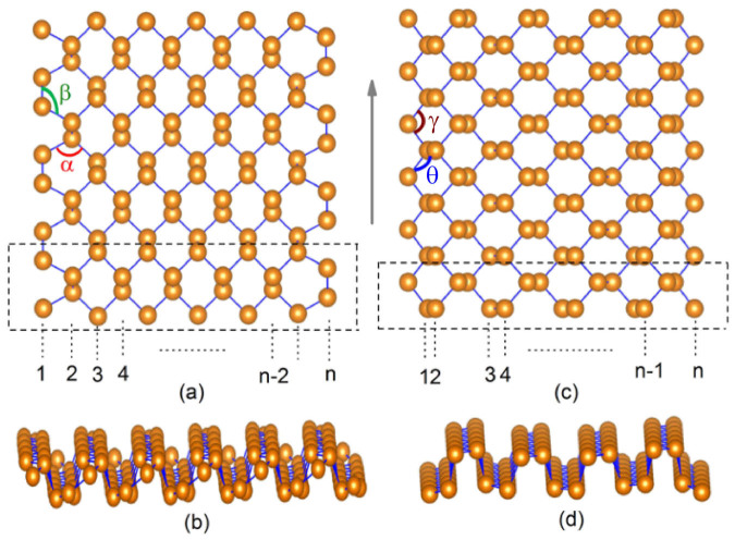
The PNRs can be obtained by cutting a monolayer phosphorene along armchair or zigzag directions. Following the conventional notation for graphene nanoribbon16, the armchair phosphorene nanoribbons (APNRs) or zigzag phosphorene nanoribbons (ZPNRs) can be identified by the number of dimer lines or the zigzag chains across the ribbon width and are labeled as N-APNRs or N-ZPNRs, respectively. Figure 1(a) and 1(c) show the ball-and-stick model of N-APNRs and N-ZPNRs, respectively. Here we consider N = 7 ~ 12 for both armchair and zigzag nanoribbons, and the width varies from about 10 Å to 26 Å. Upon structure relaxations, we see from Figure 1(b) and 1(d) there are some edge reconstructions for both APNRs and ZPNRs. Take N = 9 as an example, For the APNR, we find that the bond length between the edge atoms on the translation direction decreases from 2.26 Å to 2.06 Å. The corresponding bond angles at edge increase from 96.9° to 111.0° for α, and from 103.7° to 119.5° for β. In the case of ZPNR, the bond length at the edge decreases from 2.23 Å to 2.14 Å, and the corresponding edge angles γ and θ increase from 96.9° to 100.7°, and from 103.7° to 108.9°, respectively. Similar edge reconstructions have been also found in previous calculations17. It should be mentioned that the reconstructed motifs at the opposite edges are symmetrically arranged, which is different from those found in the BiSb nanoribbon18 with similar atomic configurations.
Figure 1.
The ball-and-stick model of armchair phosphorene nanoribbon: (a) is top-view, and (b) is side-view. The zigzag counterpart is plotted in (c) and (d), respectively. The unit cell is outlined by dash lines and the arrow indicates the translation direction of nanoribbons.
To investigate the relative stability of pristine phosphorene nanoribbons, we have computed the formation energy of both APNRs and ZPNRs. Here the formation energy EFE is defined as:
 |
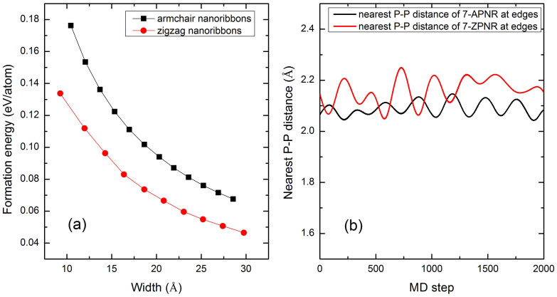
where EPNR is the calculated total energy of a given PNR, EP is the energy per atom of a phosphorene sheet, and n is the number of P atoms in the PNR. Figure 2(a) plots the formation energies of APNRs and ZPNRs as a function of the ribbon width. The small but positive formation energies indicate that the one-dimensional phosphorene nanoribbons are energetically less favorable than the two-dimensional phosphorene. Compared with the well-known graphene nanoribbons19, we find that both armchair and zigzag phosphorene nanoribbons have much smaller formation energies, suggesting that it is quite accessible to synthesize the PNRs experimentally. On the other hand, we see that the ZPNRs are energetically more favorable than the APNRs. The formation energies of both systems decrease monotonically with increasing ribbons width and converge to zero, indicating that the wider nanoribbon has relatively higher stability. To further confirm the stability of the phosphorene nanoribbons, we have performed ab-initio molecular dynamics (MD). The starting temperature is 300 K and a microcanonical ensemble has been used. The MD runs for 2000 steps with a time step of 0.5 fs. Taking 7-APNR and 7-ZPNR as an example, we show in Figure 2(b) the nearest P-P distance at the edge in the whole MD running time. We see there are only slight fluctuations around the P-P bond length of 2.06 Å for 7-APNR and 2.14 Å for 7-ZPNR, which indicates that the phosphorene nanoribbons considered in our work are rather stable.
Figure 2.
(a) The calculated formation energy of APNRs and ZPNRs as a function of the ribbon width, and (b) the ab-initio MD results of the nearest P-P distance at the edges for the 7-APNR and 7-ZPNR at room temperature.
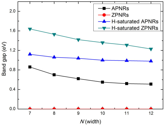
It is known that monolayer phosphorene is semiconducting with a direct band gap of 1.51 eV5. By cutting the monolayer into nanoribbons, however, we find that the ZPNRs become metallic while APNRs remain semiconducting but exhibit an indirect band gap. As indicated in Figure 3, the band gaps of APNRs decrease with increasing ribbon width, which can be attributed to the well-known quantum confinement effect20. If the edge phosphorus atoms are passivated by hydrogen atoms, our calculated results indicate that the above-mentioned edge reconstructions disappear, and the band gaps of H-saturated APNRs become direct. Moreover, there are obvious increases of the corresponding band gaps (Fig. 3). Such effect is more pronounced for the ZPNRs, where a transition from metal to indirect band gap semiconductor is observed, and the H-passivated ZPNRs exhibit the largest band gaps among the four kinds of phosphorene nanoribbons. Our results are consistent with previous works17,21 and further confirm the reliability of our calculations.
Figure 3. The calculated energy band gaps for phosphorene nanoribbons as a function of width.
We next consider the electronic transport properties of these nanoribbons by using the semiclassical Boltzmann theory and rigid-band approach22. Within this method, the chemical potential μ indicates the doping level (or carrier concentration) of the system, and the positive and negative μ correspond to n-type and p-type, respectively. The optimal carrier concentration can be obtained by integrating the density of states (DOS) of the system from the desired chemical potential to the Fermi level (μ = 0). The Seebeck coefficient S and the electrical conductivity σ are given by integration of the so-called transport distribution  :
:
 |
 |
where f0 is the equilibrium Fermi function, kB is the Boltzmann's constant, and μ is the chemical potential.  and
and  is the group velocity and relaxation time at state
  , respectively.
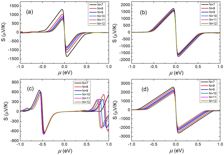
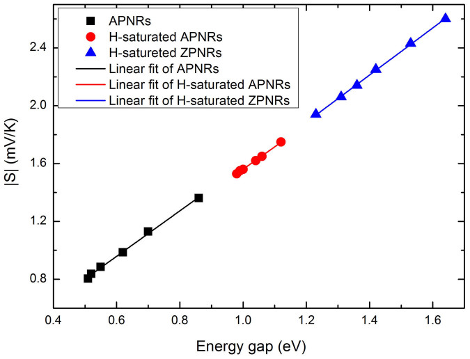
Figure 4(a) and 4(b) show the calculated Seebeck coefficients S for the APNRs and H-passivated APNRs as a function of chemical potential at room temperature, respectively. We see that by optimizing the carrier concentration, the phosphorene nanoribbons can exhibit very large value of Seebeck coefficients. As the definition of cross-sectional area has some arbitrariness for low-dimensional systems such as our phosphorene nanoribbons, in the following we will calculate the carrier concentration with respect to the interlayer distance of bulk phosphorus (3.07 Å) and the real ribbon width. For example, the pristine 7-APNR has a maximum Seebeck coefficient of 1.36 mV/K at μ = 0.056 eV. Upon edge passivation, the maximum Seebeck coefficient can further enhanced 1.75 mV/K, which is significantly higher than most of previous results23,24,25,26. As all the investigated ZPNRs in their pristine form are metallic, we see from Figure 4(c) that their Seebeck coefficients are very small around the Fermi level. However, we observe a much higher Seebeck coefficient for the H-passivated ZPNRs (Figure 4(d)), which can be optimized to 2.6 mV/K for the ZPNRs with width of N = 7. Such giant Seebeck coefficients of phosphorene nanoribbons are very beneficial for their thermoelectric applications, and we will come back to this point later. On the other hand, we find from Figure 4 that the Seebeck coefficients of three kinds of semiconducting nanoribbons exhibit obvious edge dependence, which is the largest for the H-passivated ZPNRs, the smallest for the pristine APNRs, with H-passivated APNRs in between. Such an order of Seebeck coefficients is a consequence of their distinct energy gaps. As shown in Figure 5, the Seebeck coefficient at the peak shows linear dependence with the band gap and has no trend towards to saturation. This implies that the structures which have larger band gaps would have higher Seebeck coefficients. Similar relation has also been found in the graphene/h-BN superlattice nanoribbons27.
Figure 4. The calculated Seebeck coefficient of (a) APNRs, (b) H-saturated APNRs, (c) ZPNRs, and (d) H-saturated ZPNRs as a function of chemical potential at 300 K.
Figure 5. The room temperature Seebeck coefficients (peak value) as a function of band gaps for APNRs, H-saturated APNRs, and H-saturated ZPNRs.
Within the semiclassical Boltzmann theory, the electrical conductivity σ can only be calculated with the relaxation time τ inserted as a parameter. This means that what we actually obtained is σ/τ. To figure out the electronic relaxation time of phosphorene nanoribbons, we apply the deformation potential (DP) theory proposed by Bardeen and Shockley28, where the relaxation time τ of 1D system at temperature T can be expressed as:
 |
In this formula, m* and μc are the effective mass and carrier mobility along the transport direction, respectively. The deformation potential constant E1 = ΔE/(Δl/l) is determined by changing the lattice constant l along the transport direction. The elastic modular can be obtained by C = [∂2E/∂δ2]/l, where E is the total energy of the system, δ is the applied uniaxial strain along the ribbon direction.
As the H-passivated zigzag ribbon has the largest Seebeck coefficient while it is the smallest for the pristine armchair ribbon, for simplicity, in the following we take the APNRs and H-passivated ZPNRs with width N = 7, 8, 9 as examples to discuss the thermoelectric performance of phosphorene nanoribbons. Table I lists the calculated room temperature carrier mobility μc, the relaxation time (τ), and all the related parameters indicated in Eq. (4) for the pristine armchair and H-passivated zigzag ribbons. Note that the calculated mobility for the electron can reach as high as 740 cm2/V/s at room temperature, which is higher than the experiment values of two-dimensional phosphorene FET1,2 and monolayer MoS229. The relaxation time for electron is higher than that for hole in APNRs, but it is just reversed for the H-passivated ZPNRs.
Table 1. The deformation potential E1, stretching modulus C, effective mass m*, mobility μc, and relaxation time τ for hole and electron along periodic direction in the 7, 8, 9-APNR and H-passivated 7, 8, 9-ZPNR at 300 K.
| N-PNRs | Carriers | E1 (eV) | C(eV/Å) | m* (me) | μc (cm2V−1s−1) | τ (fs) |
|---|---|---|---|---|---|---|
| 7-APNR | hole | −1.420 | 7.667 | 0.44 | 102.2 | 25.8 |
| electron | −0.826 | 7.667 | 0.65 | 168.8 | 62.9 | |
| 8-APNR | hole | −2.106 | 9.776 | 0.29 | 111.7 | 18.5 |
| electron | −1.087 | 9.776 | 0.63 | 132.4 | 47.2 | |
| 9-APNR | hole | −2.569 | 12.033 | 0.23 | 130.7 | 17.2 |
| electron | −0.512 | 12.033 | 0.62 | 740.0 | 262.5 | |
| 7-H-ZPNR | hole | −0.666 | 105.179 | 3.67 | 268.7 | 560.3 |
| electron | 3.372 | 105.179 | 1.29 | 50.1 | 36.8 | |
| 8-H-ZPNR | hole | −0.801 | 120.705 | 3.69 | 211.4 | 443.4 |
| electron | 3.492 | 120.705 | 1.30 | 52.9 | 39.2 | |
| 9-H-ZPNR | hole | −0.896 | 133.838 | 3.60 | 194.3 | 397.5 |
| electron | 3.351 | 133.838 | 1.30 | 64.3 | 47.3 |
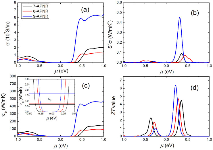
Figure 6 (a) shows the calculated electrical conductivity σ of 7, 8, 9-APNR as a function of chemical potential μ at 300 K. We see that σ of n-type is usually larger than that of p-type, especially for the 9-APNR which has a much larger electron relaxation time. For both 7-APNR and 8-APNR, we see that σ increases gradually with increasing absolute μ. However, the electrical conductivity is very small at the chemical potential where the Seebeck coefficient approach its peak value (See Fig. 4(a)). This implies that there should be a certain compromise between the Seebeck coefficient and the electrical conductivity. Indeed, we see from the Figure 6(b) that the maximum power factor (denoted by S2σ) appears at a particular chemical potential where neither the Seebeck coefficient nor the electrical conductivity reach the maximum. Among the investigated 7, 8, 9-APNR, we find that the 9-APNR exhibit the smallest Seebeck coefficient but the largest power factor (n-type), which results from its much larger electrical conductivity as discussed above. The calculated electronic thermal conductivity (κe) shown in Figure 6(c) has the same behavior as that of electrical conductivity since κe is calculated by the Wiedemann-Franz law30
 |
where the Lorentz number is set to 2.45 × 10⁻⁸ WΩK−231,32,33.
Figure 6. The calculated electronic transport coefficients at 300 K as a function of chemical potential for the 7, 8, 9-APNR: (a) the electrical conductivity, (b) the power factor, (c) the electronic thermal conductivity, and (d) the ZT value.
The straight lines in the inset of (c) indicate the lattice thermal conductivity of 7, 8, 9-APNR.
To estimate the lattice thermal conductivity (κp) of phosphorene nanoribbons, the phonon Boltzmann transport equation for the phonons are adopted47,48,49. The calculated lattice thermal conductivity of 7, 8, 9-APNR and H-passivated 7, 8, 9-ZPNR are list in the Table II. We find that the lattice thermal conductivity of both series increase with the ribbon width, which is consistent with those found in graphene nanoribbons and silicene nanoribbons34,35. In the case of APNRs, the lattice thermal conductivity are much smaller than that of bulk value (12.1 W/mK)36, implying that pristine armchair phosphorene nanoribbons may have better thermoelectric performance than their bulk counterpart. The reduced lattice thermal conductivity can be attributed to the fact that phonons in the armchair nanoribbons are different from those in bulk phosphorus because the dispersion relations will be significantly modified due to confinements in two directions. The phonon-phonon interactions can be changed and boundary scattering is much stronger in nanoribbons than in bulk system. Compared with the electronic lattice thermal conductivity (see the inset of Fig. 6(c)), the lattice part of APNRs is relatively higher in a certain chemical potential range around the Fermi level. However, the electronic part becomes dominative and increases rapidly beyond this range.
Table 2. Maximum ZT values and corresponding electron transport coefficients at optimized chemical potential (or carrier concentration n) for the 7, 8, 9-APNR and H-passivated 7, 8, 9-ZPNR at room temperature. Note for the one-dimensional PNR, the carrier concentration is calculated with respect to the interlayer distance of the bulk phosphorus (3.07 Å) and the real ribbon width.
| N-PNRs | Carrier type | μ (eV) | n (cm−3) | S (μV/K) | σ (105S/m) | S2σ (W/mK2) | κe (W/mK) | κP (W/mK) | ZT |
|---|---|---|---|---|---|---|---|---|---|
| 7-APNR | p-type | −0.36 | 5.22 × 10¹⁹ | 343.1 | 0.86 | 1.01 × 10⁻² | 0.63 | 0.67 | 2.3 |
| n-type | 0.35 | 3.71 × 10¹⁹ | −431.3 | 1.34 | 2.49 × 10⁻² | 0.98 | 34.64 | 4.5 | |
| 8-APNR | p-type | −0.28 | 4.29 × 10¹⁹ | 316.6 | 0.79 | 7.93 × 10⁻³ | 0.58 | 0.75 | 1.8 |
| n-type | 0.27 | 4.77 × 10¹⁹ | −435.7 | 1.59 | 3.02 × 10⁻² | 1.17 | 0.75 | 4.7 | |
| 9-APNR | p-type | −0.25 | 5.67 × 10¹⁹ | 270.8 | 1.20 | 8.80 × 10⁻³ | 0.88 | 1.67 | 1.0 |
| n-type | 0.21 | 2.32 × 10¹⁹ | −492.4 | 4.13 | 1.00 × 10⁻¹ | 3.03 | 1.67 | 6.4 | |
| 7-H-ZPNR | p-type | −0.79 | 5.12 × 10²⁰ | 244.2 | 17.4 | 1.04 × 10⁻¹ | 12.78 | 33.88 | 0.7 |
| n-type | 0.81 | 2.90 × 10²⁰ | −193.2 | 2.16 | 8.07 × 10⁻³ | 1.60 | 33.88 | 0.1 | |
| 8-H-ZPNR | p-type | −0.74 | 4.61 × 10²⁰ | 231.5 | 13.5 | 7.23 × 10⁻² | 9.91 | 34.64 | 0.5 |
| n-type | 0.76 | 2.34 × 10²⁰ | −193.5 | 1.97 | 7.38 × 10⁻³ | 1.45 | 34.74 | 0.1 | |
| 9-H-ZPNR | p-type | −0.69 | 4.75 × 10²⁰ | 222.4 | 12.4 | 6.11 × 10⁻² | 9.08 | 37.09 | 0.4 |
| n-type | 0.70 | 2.24 × 10²⁰ | −193.0 | 2.16 | 8.04 × 10⁻³ | 1.59 | 37.09 | 0.1 |
With all the transport coefficients available to us, we can now evaluate the ZT value of phosphorene nanoribbons, which is given by:
 |
Figure 6(d) shows the calculated ZT value of 7, 8, 9-APNR as a function of chemical potential at room temperature. We see that n-type APNRs exhibit larger ZT value than the p-type systems, which is mainly caused by relatively larger electrical conductivity and Seebeck coefficient of the former. Moreover, the peak ZT values of p-type systems decrease with increasing ribbon width, but the behavior is reversed for the n-type systems. Among the investigated APNRs, the 7-APNR shows the largest p-type ZT value of 2.3 at chemical potential μ = −0.36 eV, while the 9-APNR exhibits the largest n-type ZT value of 6.4 with μ = 0.21 eV. Such ZT values significantly exceeds the performance of most laboratory results reported and are comparable to the efficiency of traditional energy conversion method, which makes armchair phosphorene nanoribbon a very promising candidate for thermoelectric applications. As summarized in Table II, the effectiveness of the phosphorene nanoribbon is mainly due to its very large Seebeck coefficient and much lower thermal conductivity (especially the lattice part) compared with the bulk phosphorous10.
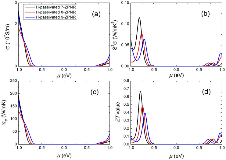
We next consider the H-passivated ZPNRs which have the largest Seebeck coefficients among the four nanoribbon series (see Fig. 4). The calculated electronic conductivity σ of 7, 8, 9-ZPNR as a function of chemical potential μ is shown in Figure 7(a). Compared with the APNRs, the obvious difference is that the p-type σ of H-passivated ZPNRs is obviously larger than that of n-type, which also leads to much larger power factor S2σ of the former (see Figure 7(b)). However, we see from Table II that H-passivated ZPNRs have obviously larger lattice thermal conductivity compared with APNRs. Similar to those observed in graphene nanoribbons34 and silicene nanoribbons35, such strong anisotropy of thermal conductivity is mainly caused by different phonon scattering rates at the zigzag and armchair edges37, and low frequency phonon bands of zigzag nanoribbons are in general more dispersive than those of the armchair nanoribbons38,39. As a result, the optimized ZT values of H-passivated ZPNRs are rather small, which is only 0.7 for the case of p-type and 0.1 for the n-type system.
Figure 7. The calculated electronic transport coefficients at 300 K as a function of chemical potential for the H-passivated 7, 8, 9-ZPNR: (a) the electrical conductivity, (b) the power factor, (c) the electronic thermal conductivity, and (d) the ZT value.
In summary, we have demonstrated that at least one type of phosphorene nanoribbons (APNRs) could be optimized to exhibit very good thermoelectric performance with a ZT value as high as 6.4 at room temperature. Our theoretical calculations are self-consistent within the framework of density functional theory and Boltzmann theory, and there are no adjustable parameters. We want to mention that the phosphorous thin films and few-layer or even monolayer phosphorene were recently fabricated by using mechanical exfoliation method1,2,3,4. It is reasonable to expect that by cutting monolayer phosphorene or by patterning epitaxially grown phosphorene, one can obtain the phosphorene nanoribbons with controllable width and/or edge, and thus realize their possible thermoelectric applications.
Methods
The electronic structure properties of PNRs are performed by using the first-principles plane-wave pseudopotential formulation40,41,42 as implemented in the Vienna ab-initio Simulation Package (VASP)43. The exchange-correlation energy is in the form of Perdew-Burke-Ernzerhof (PBE)44 with generalized gradient approximation (GGA). The cutoff energy for the wave function is set to 400 eV. For the geometry optimization, a 1 × 1 × 15 Monkhorse-Pack k-meshes45 is adopted for the Brillouin zone integration. The atomic positions are fully relaxed until the force on all atoms become less than 0.05 eV/Å. A vacuum distance of 14 Å is used for the directions of both width and thicknesses, so that the nanoribbons can be treated as independent entities. Based on the calculated energy band structure, the electronic transport properties are determined by using the semiclassical Boltzmann theory within the relaxation time approximation46. Such a method has been successfully used to predict some known thermoelectric materials, and the theoretical calculations agree well with the experimental results23,24,25,26. In order to obtain reliable transport coefficients, a denser Monkhorse-Pack k-mesh up to 125 points in the irreducible Brillouin zone (IBZ) is used. To estimate the lattice thermal conductivity of PNRs, we use the phonon Boltzmann transport equation as implemented in the so-called ShengBTE code47,48,49. For the calculations of the second-order and third-order interatomic force constant matrix, we use a 1 × 1 × 6 and 1 × 1 × 3 supercell, respectively. The interactions up to the third nearest neighbors are considered when dealing with the anharmonic one. The q-point grid and scale parameter for Gaussian smearing are set as 1 × 1 × 35 and 1.0, respectively.
Author Contributions
H.J.L. and J.S. conceived and initiated the study. J.Z. performed the calculations with helps from L.C., J.W., J.H.L. and D.D.F. J.Z. and H.J.L. analyzed the calculated results and wrote the manuscript. J.S., X.F.T. and Q.J.Z. discussed the related experimental work. All authors reviewed the paper.
Acknowledgments
We thank financial support from the National Natural Science Foundation (Grant No. 51172167 and J1210061) and the “973 Program” of China (Grant No. 2013CB632502).
References
- Liu H. et al. Phosphorene: An Unexplored 2D Semiconductor with a High Hole Mobility. ACS nano 8, 4033 (2014). [DOI] [PubMed] [Google Scholar]
- Koenig S. P., Doganov R. A., Schmidt H., Neto A. H. C. & Özyilmaz B. Electric field effect in ultrathin black phosphorus. Appl. Phys. Lett. 104, 103106 (2014). [Google Scholar]
- Li L. et al. Black phosphorus field-effect transistors. Nature Nanotech. 9, 372 (2014). [DOI] [PubMed] [Google Scholar]
- Lu W. L. et al. Plasma-assisted fabrication of monolayer phosphorene and its Raman characterization. Nano Res. 7, 853 (2014). [Google Scholar]
- Qiao J. S., Kong X. H., Hu Z. X., Yang F. & Ji W. High-mobility transport anisotropy and linear dichroism in few-layer black phosphorus. Nature Commun. 5, 4475 (2014). [DOI] [PMC free article] [PubMed] [Google Scholar]
- Keyes R. W. The electrical properties of black phosphorus. Phys. Rev. 92, 580 (1953). [Google Scholar]
- Warschauer D. Electrical and optical properties of crystalline black phosphorus. J. Appl. Phys. 34, 1853 (1963). [Google Scholar]
- Akahama Y., Endo S. & Narita S.-i. Electrical properties of black phosphorus single crystals. J. Phys. Soc. Jpn. 52, 2148 (1983). [Google Scholar]
- Morita A. Semiconducting Black Phosphorus. Appl. Phys. A: Mater. Sci. Process. 39, 227 (1986). [Google Scholar]
- Lv H. Y., Lu W. J., Shao D. F. & Sun Y. P. Large thermoelectric power factors in black phosphorus and phosphorene. arXiv:1404.5171 (2014). [Google Scholar]
- Qin G. Z. et al. Strain enhanced anisotropic thermoelectric performance of Black Phosphorus. arXiv:1406.0261 (2014). [Google Scholar]
- Hicks L. D. & Dresselhaus M. S. Effect of quantum-well structures on the thermoelectric figure of merit. Phys. Rev. B 47, 12727 (1993). [DOI] [PubMed] [Google Scholar]
- Hicks L. D. & Dresselhaus M. S. Thermoelectric figure of merit of a one-dimensional conductor. Phys. Rev. B 47, 16631 (1993). [DOI] [PubMed] [Google Scholar]
- Fei R. X. et al. Enhanced Thermoelectric Efficiency via Orthogonal Electrical and Thermal Conductances in Phosphorene. arXiv:1405.2836 (2014). [DOI] [PubMed] [Google Scholar]
- Lv H. Y., Lu W. J., Shao, D. F. & Sun, Y. P. Enhanced thermoelectric performance of phosphorene by strain-induced band convergence. arXiv:1406.5272 (2014). [Google Scholar]
- Son Y. W., Cohen M. L. & Louie S. G. Energy Gaps in Graphene Nanoribbons. Phys. Rev. Lett. 97, 216803 (2006). [DOI] [PubMed] [Google Scholar]
- Peng X. H., Wei Q. & Copple A. Edge effects on the electronic properties of phosphorene nanoribbons. arXiv:1404.5995 (2014). [Google Scholar]
- Lv H. Y. et al. The properties of BiSb nanoribbons from first-principles calculations. Nanoscale 4, 511 (2012). [DOI] [PubMed] [Google Scholar]
- Barone V., Hod O. & Scuseria G. E. Electronic Structure and Stability of Semiconducting Graphene Nanoribbons. Nano Lett. 6, 2748 (2006). [DOI] [PubMed] [Google Scholar]
- Ploog K. & Döhler G. H. Compositional and doping superlattices in III-V semiconductors. Adv. Phys. 32, 285 (1983). [Google Scholar]
- Tran V. & Yang L. Scaling laws for the band gap and optical response of phosphorene nanoribbons. Phys. Rev. B 89, 245407 (2014). [Google Scholar]
- Holland M. G. Analysis of Lattice Thermal Conductivity. Phys. Rev. 132, 2461 (1963). [Google Scholar]
- Singh D. J. & Mazin I. I. Calculated thermoelectric properties of La-filled skutterudites. Phys. Rev. B 56, R1650 (1997). [Google Scholar]
- Madsen G. K. H., Schwarz K., Blaha P. & Singh D. J. Electronic structure and transport in type-I and type-VIII clathrates containing strontium, barium, and europium. Phys. Rev. B 68, 125212 (2003). [Google Scholar]
- Singh D. J. Doping-dependent thermopower of PbTe from Boltzmann transport calculations. Phys. Rev. B 81, 195217 (2010). [Google Scholar]
- Parker D. & Singh D. J. Thermoelectric properties of AgGaTe2 and related chalcopyrite structure materials. Phys. Rev. B 85, 125209 (2012). [Google Scholar]
- Yokomizo Y. & Nakamura J. Giant Seebeck coefficient of the graphene/h-BN superlattices. Appl. Phys. Lett. 103, 113901 (2013). [Google Scholar]
- Bardeen J. & Shockley W. Deformation Potentials and Mobilities in Non-Polar Crystals. Phys. Rev. 80, 72 (1950). [Google Scholar]
- Radisavljevic B., Radenovic A., Brivio J., Giacometti V. & Kis A. Single-Layer MoS2 Transistors. Nature. Nanotech. 6, 147 (2011). [DOI] [PubMed] [Google Scholar]
- Bejan A. & Allan A. D. Heat Transfer Handbook (Wiley, New York, 2003), p. 1338. [Google Scholar]
- Zhou J. H., Jin C. G., Seol J. H., Li X. G. & Shi L. Thermoelectric properties of individual electrodeposited bismuth telluride nanowires. Appl. Phys. Lett. 87, 133109 (2005). [Google Scholar]
- Chatterjee K., Mitra M., Kargupta K., Ganguly S. & Banerjee D. Synthesis, characterization and enhanced thermoelectric performance of structurally ordered cable-like novel polyaniline-bismuth telluride nanocomposite. Nanotechnology 24, 215703 (2013). [DOI] [PubMed] [Google Scholar]
- Sumithra S. et al. Enhancement in Thermoelectric Figure of Merit in Nanostructured Bi2Te3 with Semimetal Nanoinclusions. Adv. Energy Mater. 1, 1141 (2011). [Google Scholar]
- Zheng H. et al. Enhanced thermoelectric performance of graphene nanoribbons. Appl. Phys. Lett. 100, 093104 (2012). [Google Scholar]
- Pan L. et al. Thermoelectric properties of armchair and zigzag silicene nanoribbons. Phys. Chem. Chem. Phys. 14, 13588 (2012). [DOI] [PubMed] [Google Scholar]
- Slack G. Thermal Conductivity of Elements with Complex Lattices: B, P, S. Phys. Rev. 139, A507 (1965). [Google Scholar]
- Hu J. N., Ruan X. L. & Chen Y. P. Thermal Conductivity and Thermal Rectification in Graphene Nanoribbons: A Molecular Dynamics Study. Nano Lett. 7, 2730 (2009). [DOI] [PubMed] [Google Scholar]
- Xu Y., Chen X. B., Gu B. L. & Duan W. H. Intrinsic anisotropy of thermal conductance in graphene nanoribbon. Appl. Phys. Lett. 95, 233116 (2009). [Google Scholar]
- Tan Z. W., Wang J. S. & Gan C. K. First-Principles Study of Heat Transport Properties of Graphene Nanoribbons. Nano Lett. 11, 214 (2011). [DOI] [PubMed] [Google Scholar]
- Kresse G. & Hafner J. Ab initio molecular dynamics for liquid metals. Phys. Rev. B 47, 558 (1993). [DOI] [PubMed] [Google Scholar]
- Kresse G. & Hafner J. Ab initio molecular-dynamics simulation of the liquid-metal-amorphous-semiconductor transition in germanium. Phys. Rev. B 49, 14251 (1994). [DOI] [PubMed] [Google Scholar]
- Kresse G. & Furthmüller J. Efficiency of ab-initio total energy calculations for metals and semiconductors using a plane-wave basis set. Comput. Mater. Sci. 6, 15 (1996). [DOI] [PubMed] [Google Scholar]
- Kresse G. & Furthmüller J. Efficient iterative schemes for ab initio total-energy calculations using a plane-wave basis set. Phys. Rev. B 54, 11169 (1996). [DOI] [PubMed] [Google Scholar]
- Perdew J. P., Burke K. & Ernzerhof M. Generalized Gradient Approximation Made Simple. Phys. Rev. Lett. 77, 3865 (1996). [DOI] [PubMed] [Google Scholar]
- Monkhorst H. J. & Pack J. D. Special points for Brillonin-zone integrations. Phys. Rev. B 13, 5188 (1976). [Google Scholar]
- Madsen G. K. H. & Singh D. J. BoltzTraP. A code for calculating band-structure dependent quantities. Comput. Phys. Commun. 175, 67 (2006). [Google Scholar]
- Li W., Carrete J., Katcho N. A. & Mingo N. ShengBTE: A solver of the Boltzmann transport equation for phonons. Comput. Phys. Commun. 185, 1747 (2014). [Google Scholar]
- Li W. et al. Thermal conductivity of diamond nanowires from first principles. Phys. Rev. B 85, 195436 (2012). [Google Scholar]
- Li W., Lindsay L., Broido D. A., Stewart D. A. & Mingo N. Thermal conductivity of bulk and nanowire Mg2SixSn1−x alloys from first principles. Phys. Rev. B 86, 174307 (2012). [Google Scholar]


