Abstract
Two-dimensional metasurface structures have recently been proposed to reduce the challenges of fabrication of traditional plasmonic metamaterials. However, complex designs and sophisticated fabrication procedures are still required. Here, we present a unique one-dimensional (1-D) metasurface based on bilayered metallic nanowire gratings, which behaves as an ideal polarized beam splitter, producing strong negative reflection for transverse-magnetic (TM) light and efficient reflection for transverse-electric (TE) light. The large anisotropy resulting from this TE-metal-like/TM-dielectric-like feature can be explained by the dispersion curve based on the Bloch theory of periodic metal-insulator-metal waveguides. The results indicate that this photon manipulation mechanism is fundamentally different from those previously proposed for 2-D or 3-D metastructures. Based on this new material platform, a novel form of metasurface holography is proposed and demonstrated, in which an image can only be reconstructed by using a TM light beam. By reducing the metamaterial structures to 1-D, our metasurface beam splitter exhibits the qualities of cost-efficient fabrication, robust performance, and high tunability, in addition to its applicability over a wide range of working wavelengths and incident angles. This development paves a foundation for metasurface structure designs towards practical metamaterial applications.
Introduction
Metamaterials with metallic structures have been demonstrated to exhibit unique electromagnetic properties that are not available naturally, such as extraordinary transmission beyond the diffraction limit1,2, efficient light-harvesting ability3,4, plasmonic color filtering5,6,7, and, most notably, controlling the reflection or transmission direction of a light beam8,9,10. However, multi-layered three-dimensional (3-D) metamaterials suffer from complicated and costly fabrication, a narrow usable bandwidth due to their resonant character, and low optical efficiency due to the inherent metal absorption. Recently, metasurfaces have been proposed to overcome these issues by reducing the dimensionality to a two-dimensional (2-D) meta-platform. With this newly proposed meta-platform, applications of the photonic spin-Hall effect11, polar metalensing12, and light bending13,14,15, previously observed in 3-D metamaterials, have been successfully demonstrated. However, these 2-D metasurfaces still require precise arranging of the directions and shapes of their resonant antenna units to obtain a gradient refractive index. In this work, we further simplify the metastructure to a one-dimensional (1-D) metasurface using a type of bilayer metallic nanowire grating, which leads to not only much easier fabrication, but also better performance in producing polarized negative reflection, as reported for some 2-D metasurfaces13,14,15. Here, we refer to reflection into the negative first diffractive order as “Negative reflection (NR)” and reflection into the zero diffractive order as “Reflection (R)”. Consequently, an efficient approach for fabricating novel polarized beam splitters (PBSs) is presented here.
Previously, metallic nanowire gratings have been demonstrated as PBSs in liquid crystal displays (LCDs)16,17,18,19, having the advantages of high optical efficiencies and large extinction ratios compared with conventional PBSs fabricated from absorptive dichroic polymer films20, bulky birefringent crystals21, multilayer interference laminas22, and dielectric gratings23. However, thus far, these studies have only focused on the transmission and reflection properties, while polarized diffraction has not been considered. In this work, we propose the use of bilayer metallic nanowire gratings with nano-slits as 1-D metamaterials to realize both polarized negative reflection and reflection. The dispersion curves of the periodical nano-slit-waveguided modes are calculated based on waveguide theory24,25,26 to reveal their TM-dielectric-like/TE-metallic-like character and thus the polarized negative reflection and reflection properties of the nano-optical material structures. We refer to this feature as “metasurface beam splitting”. Metasurface beam splitting does not rely on a resonant coupling mechanism and therefore enables a broad range of useable wavelengths and incident angles, with flexible tunability in operation.
Furthermore, as an example of a potential application, by combining the intrinsically fringed structure of a hologram and the anisotropic character of metasurface beam splitter, a metasurface holograph, ‘decodable’ only by TM light, is proposed and presented. Thus, a higher-security anti-counterfeit hologram is produced by adding the additional criterion of polarization dependence.
Structure design and fabrication
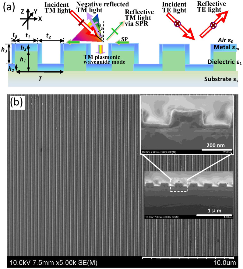
A schematic of the proposed metasurface beam splitter is presented in Fig. 1(a), where the effects of polarized beam splitting are illustrated. The longitudinal plasmonic slit-waveguide mode is denoted by a perpendicular arrow, which represents the primary physical component responsible for the splitting function. The lateral surface plasmon resonance (SPR) is denoted by the horizontal arrows, which leads to reflection peak for TM light.
Figure 1. Structure of the metasurface beam splitter.
(a) Schematic diagram. TM light enters the slits in plasmonic waveguide mode and is reflected by the bottom Al layer. The light is strongly negatively reflected, as indicated by the chromatic sector. The reflection includes light corresponding to lateral SPR, as shown by green arrow, and light in the non-diffraction zone shown in Fig. 2(b1) and Fig. 3(b1). TE light cannot enter the slits and is primarily reflected. (b) SEM images of the top and side views (insets) of the fabricated device. The grating pitch is T = 420 nm, the width of the dielectric PMMA is t1 = 170 nm, and the width of the metal Al in the bottom PMMA-Al grating layer is t2 = 250 nm. The thicknesses of the PMMA and Al are h1 = 110 nm and h2 = 30 nm, respectively. The size of the Al on the sidewalls of the PMMA grating lines is t3 × h3 = 20 nm × 110 nm. The substrate is silicon.
Scanning electron microscopy (SEM) images of the top and side views of the fabricated device are shown in Fig. 1(b). A polymethyl methacrylate (PMMA) grating with a pitch of 420 nm and 170-nm-wide bars was fabricated by nano-imprinting on a silicon substrate. The height of the PMMA reliefs was h1 = 110 nm. Then, the nano-imprinted grating was deposited with an aluminum (Al) film of thickness h2 = 30 nm by electron beam (E-beam) evaporation. In addition to the two layers of Al formed on the top of the PMMA ridges and in the grooves, the sidewalls of the PMMA bars were also coated with Al, as shown in Fig. 1(a).
Metasurface beam splitter
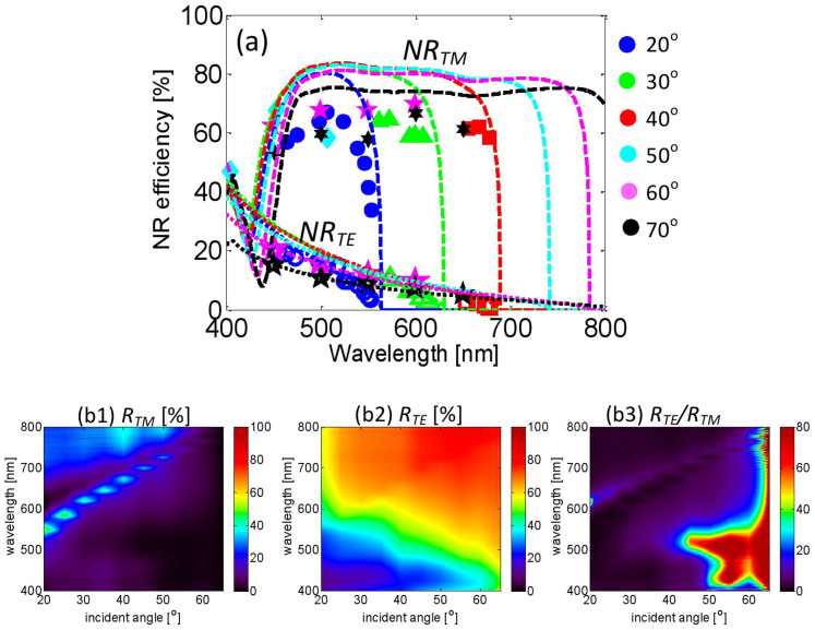
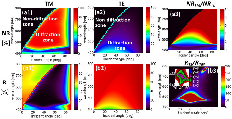
The NR spectra, as shown in Fig. 2(a) for experiments and Figs. 3(a1–a2) for simulations, clearly show a range termed diffraction zone, where TM light is strongly negatively reflected and the TE negative reflection is weak and decreases sharply with increasing wavelength. The distinct boundaries of the diffraction zone are the maximum negative first-order diffraction wavelengths of the grating, with G = T*(1+sin i), where T is the grating pitch and i is the incident angle of the light beam. As the incident angle increases, the diffraction zone extends to longer wavelengths; consequently, the working spectral band can be tuned. The TM reflection spectra, as shown in Fig. 2(b1) for experiments and Fig. 3(b1) for simulations, exhibit a single peak arising from lateral SPR at the Al/air interface. Only TM light with a wavelength longer than the SPR peak wavelength is notably reflected, while TE light is strongly reflected throughout the entire visible light region at all incident angles for both experiments and simulations, as shown in Fig. 2(b2) and Fig. 3(b2). Thus, the device functions as a TM-NR/TE-reflection PBS for light in the diffraction zone. For example, for light with a wavelength of 500 nm and an incident angle of 55°, the measured NR efficiencies for TE and TM light, NRTM and NRTE, are 82% and 15%, respectively. The measured reflection efficiencies for TE and TM light, RTE and RTM, are 55% and 0.4%, respectively. As the incident angle increases, the PBS exhibits reflectivity over a broader band of wavelengths. In particular, at incident angles larger than 70°, PBS reflectivity can be achieved throughout the entire visible light range.
Figure 2. NR and reflection spectra.
(a) NR spectra for incident angles from 20° to 70°. The different colors denote different incident angles. The solid and hollow markers indicate measured results for TM and TE light, respectively. The dashed and dotted lines correspond to simulated results for TM and TE light, respectively, which are selected from Fig. 3(a1–a2). (b1–b3) Measured reflection spectra of (b1) TM light and (b2) TE light and (b3) the corresponding extinction ratios of RTE/RTM. The colors in (b1) and (b2) are the fraction of incident power going into NR or R in percentage. These results show that NRTM is much larger than NRTE, while RTE is larger than RTM. The operational spectrum expands to the entire visible light range for an incident angle of 70°. The TM reflection exhibits a single peak arising from SPR at the interface of Al and air.
Figure 3. Simulated spectra.
(a1) – (a3) The simulated NR spectra for (a1) TM light and (a2) TE light and (a3) the extinction ratio of NRTM/NRTE, (b1–b3) The simulated reflection spectra for (b1) TM light and (b2) TE light and (b3) the extinction ratio of RTE/RTM. The colors in (a1–a2) and (b1–b2) are the fraction of incident power going into NR or R in percentage. The cyan dashed lines in (a1) and (a2) represent the boundary between the diffraction zone and the non-diffraction zone. The red dotted line in (b1) represents the SPR wavelengths. The inset in (b3) shows the high extinction ratio zone in detail. The structure used in this simulation is the same as that of the fabricated device shown in Fig. 1.
An extinction ratio of RTE/RTM > 80 was measured for wavelengths from 420 nm to 520 nm and incident angles from 50° to 65°, as shown in Fig. 2(b3). For the simulations shown in Fig. 3(b3), the extinction ratio of RTE/RTM is greater than 300 for a wide range of incident angles (20°–70°) and for a bandwidth of approximately 100 nm. Furthermore, the ratio reaches 106 at a wavelength of 500 nm and an incident angle of 45°. Although the extinction ratios NRTM/NRTE, as shown in Fig. 3(a3), are just above 10 for wavelengths larger than 550 nm, higher extinction ratios can be obtained, for example, by reducing the slit width, as demonstrated in Supplementary Fig. 1.
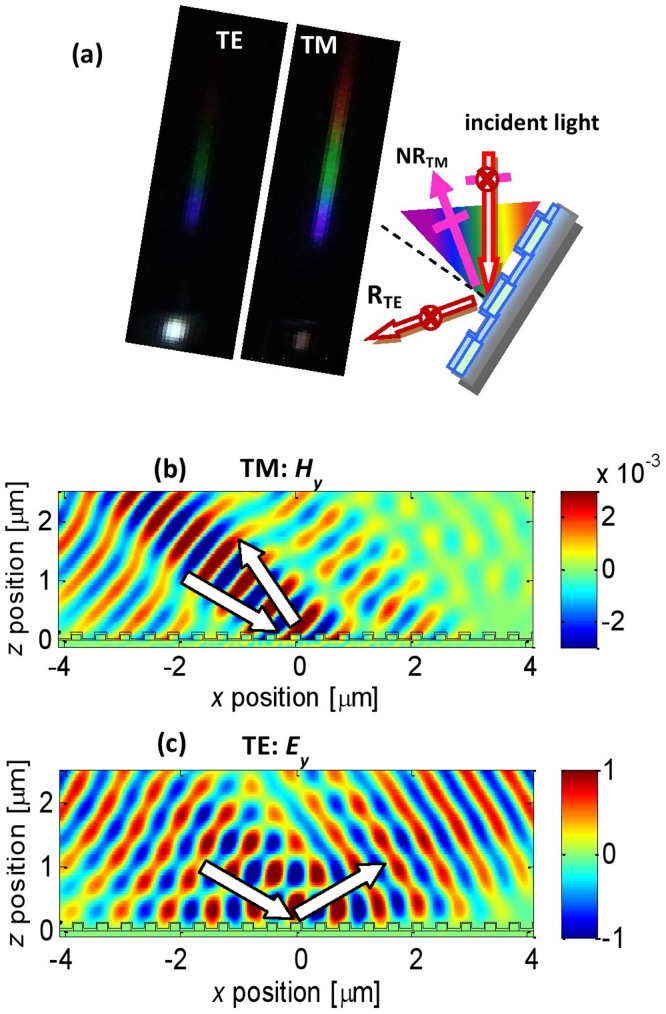
Figure 4(a) shows the experimental far-field patterns of NR and reflection for an incident angle of 55°, providing a visualization of the metasurface beam splitting characteristics. The reflected TE light is bright white light, indicating intense broadband reflectance, while the reflected TM light is faint dark red, implying low narrowband reflectance. Data for other incident angles and corresponding videos are available online (Supplementary Fig. 2 and Videos 1–3), which demonstrate the alternating intensity and color shifts of the NR and reflection as the incident light polarization is rotated. The near-field distributions shown in Figs. 4(b) and 4(c), obtained by using the finite-difference time-domain method (FDTD Solutions, Lumerical), clearly show the metasurface beam splitting. Supplementary Videos 4–5 vividly display these two processes.
Figure 4. Far- and near-field distributions.
(a) Images of NR and reflection for TE and TM white light, respectively, for an incident angle of 55° in the experiment. The TM light is strongly negatively reflected as a rainbow of colors while the TE light is primarily reflected as white light. Panels (b) and (c) display the time snapshots of the simulated magnetic field Hy for TM light and the electric field Ey for TE light, respectively, for a wavelength of 500 nm and an incident angle of 55°. The incident, NR, and reflected light are depicted by the white arrows, respectively. The black lines schematically depict the profile of the bilayer grating. The structure used in the simulation is the same as that of the fabricated device shown in Fig. 1. The magnitude of the incident electric field is 1.0.
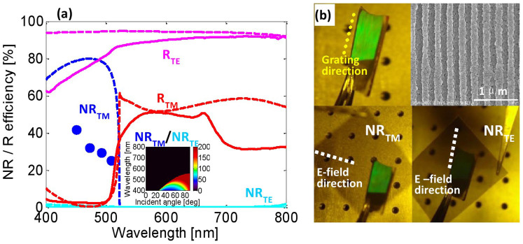
To further demonstrate the flexible tunability of the devices, the measured and simulated results of a bilayer metallic nanowire grating fabricated by laser interference lithography on a BK7 glass substrate with a pitch of 280 nm and a PMMA line width of 140 nm are presented in Fig. 5. For this device, the thickness h2 of the deposited Al is 50 nm, and the sidewall width t3 is approximately 30 nm. It is clear that compared with above case, the upper and lower limits of the diffraction zone are blue-shifted and that NRTE is reduced because the slit width is only 80 nm. Extinction ratio values of NRTM/NRTE = 150 and RTE/RTM = 30 at a wavelength of 450 nm were obtained in the experimental measurements. In the simulations, the extinction ratios for both reflection and NR exceeded 100 over a broad wavelength range, as shown in the insets of Fig. 5(a) and Supplementary Fig. 3. The polarized NR is clearly shown in the photos in Fig. 5(b).
Figure 5. Spectra and photos of a 280-nm-pitch grating.
(a) Measured (solid lines) and simulated (dashed lines) NR (blue and cyan lines) and reflection (red and magenta lines) spectra for TM (blue and red lines) and TE (cyan and magenta lines) light with an incident angle of 60°. The inset is the simulated extinction ratio of NRTM/NRTE. (b) Photos of the device irradiated by un-polarized white light with an incident angle of approximately 60° and filtered by a polyvinyl alcohol (PVA) plastic polarizer (extinction ratio of 300). The yellow dotted line indicates the direction of the grating lines. The white dashed lines illustrate the electric field direction of the light passing through the polarizer. An SEM image of the device is also presented. The dielectric grating in the device was fabricated by laser interference, with an Al thickness of 50 nm.
Using the Bloch theory of periodic waveguides, the TM and TE dispersion curves28 of the dominant first-order waveguide mode for an Al-air grating with a 420-nm pitch and a slit width of 60–210 nm were calculated, as shown in Figs. 6(a) and 6(b), respectively. It is clear that for TM light, plasmonic waveguide modes (blue lines) exist below the light cone (black solid line), with a negligible imaginary part of the wave vector along the z-axis kz (red lines). By contrast, for TE light, the first-order mode is above the light cone with a significant imaginary component of kz, increasing with decreasing frequency . The frequency (wavelength) at which the imaginary part of kz is equal to the real part is called the cut-off frequency (wavelength) and represents the dissipation strength. The solid line represents the result for our experiments and corresponds to the simulation with a cut-off wavelength c = 480 nm. For shorter-wavelength light, the normal waveguide mode exists in the air slits; therefore, some diffraction is obtained, as shown in Figs. 2(a) and 3(a2), which fades rapidly with increasing wavelength. As the slit width is reduced, the TE cut-off wavelength c is blue-shifted, indicating a stronger dissipation effect. Figure 6(b) shows that for a slit narrower than 160 nm, all visible light with a wavelength longer than 400 nm can barely enter the slits.
Figure 6. Dispersion curves.
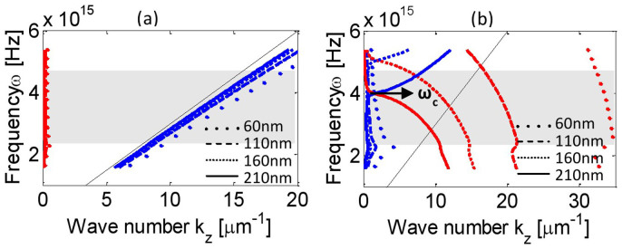
(a) Dispersion curves of the first-order longitudinal Bloch plasmonic waveguide modes in Al-air-Al slits for (a1) TM and (a2) TE light. The blue and red lines of various line types represent the real and imaginary parts of the wave vector kz for slit widths of 60 nm to 210 nm, respectively. The black solid line represents the light cone.
In accordance with the plasmonic waveguide model, it is clear from Fig. 4(c) that the TE light is mostly reflected, with little penetration into the slits due to the cut-off effect of the slits. By contrast, as shown in Fig. 4(b), TM light can efficiently pass through the first layer of the metal grating and is then reflected by the bottom Al layer. Although the TM reflectance will be increased by the bottom Al grating in our bilayer structure metasurface, by utilizing destructive Fabry-Perot (F-P) resonance between the two metal films to inhibit the TM reflection, most of the TM light is diffracted, and high values of RTE/RTM and NRTM/NRTE can still be obtained. The field distribution in Fig. 4(b) clearly shows these two aspects: the low reflection of the first layer of the metal grating and the destructive interference of the F-P resonance between the two layers of the metal grating, which result in the overall low TM reflection. The simulated results presented in Fig. 3(b3) show the minimum RTM and maximum RTE/RTM at resonant wavelength of 485 nm. This resonant wavelength can be tuned by changing the values of the slit width and thickness h1. An example with a slit width of 100 nm and h1 = 125 nm is shown in Supplementary Fig. 1, where RTE/RTM reaches 106 at a resonant wavelength of 620 nm. Furthermore, for this narrower slit, the TE diffraction is further reduced and the reflection increased. This case results in both extinction ratios NRTM/NRTE and RTE/RTM being over 100 in the simulations, as shown in Supplementary Fig. 1.
Metasurface holography
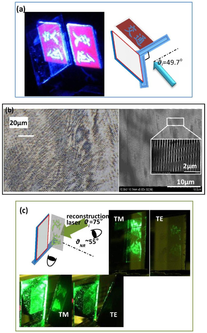
Using SPR based on a diffraction grating and the metallic antenna effect, several plasmonic holograms have been demonstrated29,30. However, for such reported resonant-type devices, the incident angle or laser wavelength is limited to a narrow working range. However, using a non-resonant metasurface beam splitter, we can produce holograms that operate over a broad range of wavelengths and incident angles. A photoresist hologram of Shanghai Jiao Tong University's school badge “ ” was produced by laser interference lithography, as shown in Fig. 7(a). The hologram was then coated with a 50-nm-thick Al layer. The microscopy images in Fig. 7(b) show that the sample consists of randomly distributed bilayer metallic nanowire gratings with a pitch of 300 nm. The photos in Fig. 7(c) clearly show that only TM light can reconstruct the real image of “
 ” which corresponds to the negative first-order diffraction mode (NR) of the bilayer metallic nanowire grating. Supplementary Videos 6 and 7 vividly display the clarity of the reconstructed image upon changes in the incident light polarization. Thus, a novel metasurface hologram with an inherent anti-counterfeiting quality is achieved with the additional verification of its polarization dependence.
Figure 7. Metasurface hologram.
(a) Photoresist hologram fabrication scheme: The badge was placed perpendicularly to the photoresist film, and both were illuminated by a large cross-section collimated laser beam with an incident angle of 49° to the photoresist film. (b) Microscopy and SEM images of the top views of the metasurface hologram film at different scales. The film consists of randomly distributed B-MNGs with a pitch of 300 nm. The width of the dielectric PMMA is t1 = 150 nm, and the thicknesses of the PMMA and Al are h1 = 110 nm and h2 = 50 nm, respectively. (c) Real images reconstructed using TM and TE laser light, respectively. The metasurface hologram was illuminated by a TM or TE laser with a wavelength of 532 nm and an incident angle of 75°. The reconstructed real 3-D image was formed by the negative first-order diffraction mode with a diffractive angle of 55° and was imaged onto a black screen, as presented in the bottom left pictures. The image was also viewed with a camera, as presented in the top right pictures, or directly by eye.
Discussion
In general, diffraction occurs when the incident wavelength is comparable to the pitch of a grating. However, this is not the case for metallic gratings. It has been found that the cut-off effect of plasmonic waveguide arrays not only prohibits the transmission of TE light, but also causes the disappearance of TE diffraction. By contrast, the TM light remains and is even highly diffracted beyond the diffraction limit for a slit. The large anisotropy resulting from this TE-metal-like/TM-dielectric-like feature can be explained by the dispersion curve based on the Bloch theory of periodic metal-insulator-metal waveguides. We have demonstrated an ultra-compact TM-NR/TE-reflection metasurface beam splitter with excellent performance characteristics such as high efficiency and compatibility over a broad range of wavelengths and incident angles. In general, such a beam splitter can be designed using the following guidelines: (1) The slit width determines the lower wavelength limit due to the cut-off effect on TE light. (2) The grating pitch determines the upper wavelength limit of the diffraction zone. For wavelengths between the cut-off and the upper limit, TE diffraction is very weak and rapidly decreases for longer wavelengths, while TM light is substantially negatively reflected. (3) With proper slit height selection, TM reflection can be further inhibited by destructive F-P resonance of the plasmonic slit-guided mode, significantly enhancing the reflective polarization extinction ratio RTE/RTM.
In summary, by integrating diffraction, waveguide, and plasmonic effects, we propose a novel method for controlling photons with a 1-D metasurface, which is fundamentally different from methods previously proposed for 2-D or 3-D metastructures. A unique and robust PBS with a 1-D metasurface has been demonstrated, which is applicable over a wide range of working wavelengths and incident angles, making it ideal for practical beam splitting devices. As an application, we have demonstrated for the first time a unique metasurface hologram, which can be reconstructed only with TM light, thereby increasing the difficulty of producing a counterfeit. As a cost-efficient and robust metastructure, the 1-D device has the potential to be used in a broad range of applications including displays, holograms, and laser optics.
Methods
Device fabrication
PBS-1
A PMMA (Allresist, German) dielectric grating with a pitch of 420 nm and a bar width of 170 nm was fabricated by nano-imprinting on a silicon substrate. The grating was subsequently coated with a 30-nm-thick Al film by E-beam evaporation.
PBS-2
A PMMA dielectric grating with a pitch of 280 nm and a bar width of 140 nm was fabricated by laser interference using a He–Cd laser (442 nm, KIMMON) with a cross angle of 52° on a BK7 glass substrate. The grating was then coated with a 50-nm-thick Al film by E-beam evaporation.
Metasurface hologram
A photoresist hologram of Shanghai Jiao Tong University's school badge “ ” was produced by laser interference lithography. The badge was placed perpendicularly to the photoresist film, and both were illuminated by a large cross-section collimated laser beam with an incident angle of 49.7° to the photoresist film. The photoresist hologram was subsequently coated with a 50-nm-thick Al film by E-beam evaporation.
Diffraction images and spectral measurement
PBS characterization
Unpolarized white light from a white light LED was focused by a 20X objective lens and then collimated and polarized by a convex lens and a Glan-Thomson prism, respectively. Finally, the light was directed to a device fixed on a motor-driven rotating stage. The diffracted and reflected light was collected by a fiber mounted with a collimating lens connected to a spectrometer (QE65-PRO, Ocean Optics). As the diffraction and reflection patterns were displayed on a white screen, the Glan-Thomson prism was continuously rotated to change the polarization state of the incident light.
Metasurface hologram reconstruction
The metasurface hologram was illuminated by a TM or TE laser with a wavelength of 532 nm and an incident angle of 75°. The reconstructed real 3-D image was formed by the negative first-diffraction order (NR) with a diffractive angle of 55°. The image was either displayed on a black screen or viewed directly by eye or through a camera.
Simulation methods
The simulated spectra in Figs. 2, 3, and 5 were obtained using 2-D rigorous coupled-wave analysis (Diffract MODE, RSOFT). TM or TE light was incident from top to bottom with an incident angle of 0° to 90° in steps of 0.2°. The incident light had wavelengths of 400 nm to 800 nm in steps of 2 nm. Five harmonics were used in representing the eigen-mode expansion of the slits. The grid size was 1 nm. The permittivity of PMMA is ε1 = 2.56. The permittivity of Al and the permittivity of Si substrate are taken from this software's material library. The permittivity of glass substrate in Fig. 5 is 2.25.
The simulated electromagnetic field distributions in Fig. 4 and Videos 4–5 in the Supplementary Material were produced using the finite-difference time-domain method (FDTD Solutions, Lumerical), where 21 periods of the grating were taken and the absorbed boundary condition was set in both the x and z directions. The grid step size was 2 nm. The incident wavelength was 500 nm, and the incidence angle was 55°. The permittivity of PMMA is ε1 = 2.56. The permittivity of Al εm and the permittivity of Si substrate εs are taken from this software's material library. The dispersion curves of the longitudinal waveguide modes in the air slits, as shown in Fig. 6(a) and 6(b), are obtained from the following equation according to the theory of periodic waveguides:
 |
Where, K denotes the Bloch wave number; the grating pitch T = d1 + d2; d1 = 210 nm and d2 = 210 nm are the width of the aluminum and air in one pitch, respectively; k1 = (k0ε1-kz_1)1/2 and k2 = (k0ε2-kz_2)1/2 are the wave number of the waveguide mode in the aluminum and air long the x-axis, respectively; kz is the wave number along the z-axis; k0 is the wave number of the light in air; g = k1ε2/(k2ε1) for TM light and k1/k2 for TE light, respectively. The permittivity of air ε1 = 1. The permittivity of Al ε2 is calculated the equation induced by the Lorantz-Drude mode in Ref. 27:
 |
where ω is the light frequency, ωp is the plasma frequency, k is the number of oscillators with frequency ωj, strength fj, and lifetime 1/Γj, while Ωp = (f0)0.5ωp is the plasma frequency associated with intraband transitions with oscillator strength f0 and damping constant Γ0. These parameters are also taken from this reference: ωp = 14.98*2πh, f 0-4 = [0.523, 0.227, 0.050, 0.166, 0.030]; Γ0-4 = [0.047, 0.333, 0.312, 1.351, 3.382]* 2πh, ω0-4 = [0.000, 0.162, 1.544, 1.808, 3.473]*2πh.
Author Contributions
J.Z. performed the device measurement, conducted the simulations, and wrote the main manuscript text. Z.C.Y. was responsible for project management, fabricated the samples, performed the device measurement and wrote the main manuscript text. N.L.S. and R.Z. developed the measurement setup and performed the measurements. Z.M.S., H.P.D.S., and J.Z. contributed to analyze the results and write the manuscript. All authors reviewed the manuscript.
Supplementary Material
Video 1
Video 2
Video 3
Video 4
Video 5
Video 6
Video 7
Supplementary Figures
Acknowledgments
This work was supported by the National Natural Science Foundation of China (Nos. 61370047, 11374212, 61007025, 51235007 and 11121504), the Ph.D. Programs Foundation of the Ministry of Education of China (No. 20100073120034), the Major State Basic Research Development Program (2013CB328804) and the Key Laboratory of High Energy Laser Science and Technology, China Academy of Engineering Physics (2012HCF03).
References
- Ebbesen T. W. et al. Extraordinary optical transmission through sub-wavelength hole arrays. Nature 391, 667–669 (1998). [Google Scholar]
- Martín-Moreno L. et al. Theory of extraordinary optical transmission through subwavelength hole arrays. Phys. Rev. Lett. 86, 1114–1117 (2001). [DOI] [PubMed] [Google Scholar]
- Atwater H. A. & Polman A. Plasmonics for improved photovoltaic devices. Nat. Mater. 9, 205–213 (2010). [DOI] [PubMed] [Google Scholar]
- Pala R. A. et al. Optimization of non-periodic plasmonic light-trapping layers for thin-film solar cells. Nat. Commun. 4, 2095, 10.1038/ncomms3095 (2013). [DOI] [PubMed] [Google Scholar]
- Yokogawa S., Burgos S. P. & Atwater H. A. Plasmonic color filters for CMOS image sensor applications. Nano Lett. 12, 4349–4354 (2012). [DOI] [PubMed] [Google Scholar]
- Laux E., Genet C., Skauli T. & Ebbesen T. W. Plasmonic photon sorters for spectral and polarimetric imaging. Nat. photonics 2, 161–164 (2008). [Google Scholar]
- Xu T., Wu Y. K., Luo X. G. & Guo L. J. Plasmonic nanoresonators for high-resolution colour filtering and spectral imaging. Nat. Commun. 1, 59; 10.1038/ncomms1058 (2010). [DOI] [PubMed] [Google Scholar]
- Valentine J. et al. Three-dimensional optical metamaterial with a negative refractive index. Nature 455, 376–379 (2008). [DOI] [PubMed] [Google Scholar]
- Liu N. et al. Three-dimensional photonic metamaterials at optical frequencies. Nat. Mater. 7, 31–37 (2008). [DOI] [PubMed] [Google Scholar]
- Monticone F., Estakhri N. M. & Alù A. Full Control of Nanoscale Optical Transmission with a Composite Metascreen. Phys. Rev. Lett. 110, 203903(2013). [DOI] [PubMed] [Google Scholar]
- Yin X. B. et al. Photonic Spin Hall Effect at Metasurfaces. Science 339, 1405–1407 (2013). [DOI] [PubMed] [Google Scholar]
- Chen X. Z. et al. Dual-polarity plasmonic metalens for visible light. Nat. Commun. 3, 1198; 10.1038/ncomms2207 (2012). [DOI] [PMC free article] [PubMed] [Google Scholar]
- Ni X. et al. Broadband light bending with plasmonic nanoantennas. Science 335, 427 (2012). [DOI] [PubMed] [Google Scholar]
- Yu N. F. et al. Light propagation with phase discontinuities: generalized laws of reflection and refraction. Science 334, 333–337 (2012). [DOI] [PubMed] [Google Scholar]
- Pors A., Albrektsen O., Radko I. P. & Bozhevolnyi S. I. Gap plasmon-based metasurfaces for total control of reflected light. Sci. Rep. 3, 2155; 10.1038/srep02155 (2013). [DOI] [PMC free article] [PubMed] [Google Scholar]
- Yu Z. et al. Reflective polarizer based on a stacked double-layer subwavelength metal grating structure fabricated using nanoimprint lithography. Appl. Phys. Lett. 77, 927–929 (2000). [Google Scholar]
- Ge Z. B. & Wu S. T. Nanowire grid polarizer for energy efficient and wide-view liquid crystal displays. Appl. Phys. Lett. 93, 121104-1-3 (2008). [Google Scholar]
- Kim S. H., Park J. D. & Lee K. D. Fabrication of a nano-wire grid polarizer for brightness enhancement in liquid crystal display. Nanotechnology 17, 4436–4438 (2006). [Google Scholar]
- Oh J. H. et al. Stereoscopic TFT-LCD with wire grid polarizer and retarder. SID' 08 39, 444–447 (2008). [Google Scholar]
- Kawatsuki N. & Fujio K. Cooperative reorientation of dichroic dyes dispersed in photo-cross-linkable polymer liquid crystal and application to linear polarizer. Chem. Lett. 34, 558–559 (2005). [Google Scholar]
- Li L. & Dobrowolski J. A. Visible broadband, wide-angle, thin-film multilayer polarizing beam splitter. Appl. Opt. 35, 2221–2225 (1996). [DOI] [PubMed] [Google Scholar]
- Weber M. F. et al. Giant birefringent optics in multilayer polymer mirrors. Scinece 287, 2451–2456 (2000). [DOI] [PubMed] [Google Scholar]
- Zheng J. J., Zhou C. H., Feng J. J. & Wang B. Polarizing beam splitter of deep-etched triangular-groove fused-silica gratings. Opt. Lett. 33, 1554–156 (2008). [DOI] [PubMed] [Google Scholar]
- Liu H. T. & Lalanne P. Microscopic theory of the extraordinary optical transmission. Nature 452, 728–731 (2008). [DOI] [PubMed] [Google Scholar]
- Le Perchec J., Quémerais P., Barbara A. & López-Ríos T. Why metallic surfaces with grooves a few nanometers deep and wide may strongly absorb visible light. Phys. Rev. Letts. 100, 066408 (2008). [DOI] [PubMed] [Google Scholar]
- Wu Y. R., Hollowell A. E., Zhang C. & Guo L. J. Angle-insensitive structural colours based on metallic nanocavities and coloured pixels beyond the diffraction limit. Sci. Rep. 3, 1194; 10.1038/srep01194 (2013). [DOI] [PMC free article] [PubMed] [Google Scholar]
- Rakić A. D., Djuriši ć A. B., Elazar J. M. & Marian L. Majewski M. L. Optical properties of metallic films for vertical-cavity optoelectronic devices. Appl. Opt. 37, 5271–5283 (1998). [DOI] [PubMed] [Google Scholar]
- Ye Z. C. et al. Compact transreflective color filters and polarizers by bi-layer metallic nanowire gratings on flexible substrates. IEEE J. Sel. Top. Quant. 19, 4800205-1-5 (2013). [Google Scholar]
- Ozaki M., Kato J. & Kawata S. Surface-Plasmon Holography with White-Light Illumination. Science 332, 218 (2011). [DOI] [PubMed] [Google Scholar]
- Huang L. L. et al. Three-dimensional optical holography using a plasmonic metasurface. Nat. COMM. 4, 2808 (2014). [Google Scholar]
Associated Data
This section collects any data citations, data availability statements, or supplementary materials included in this article.
Supplementary Materials
Video 1
Video 2
Video 3
Video 4
Video 5
Video 6
Video 7
Supplementary Figures


