Abstract
Graphene emerges as a viable material for optoelectronics because of its broad optical response and gate-tunable properties. For practical applications, however, single layer graphene has performance limits due to its small optical absorption defined by fundamental constants. Here, we demonstrated a new class of flexible electrochromic devices using multilayer graphene (MLG) which simultaneously offers all key requirements for practical applications; high-contrast optical modulation over a broad spectrum, good electrical conductivity and mechanical flexibility. Our method relies on electro-modulation of interband transition of MLG via intercalation of ions into the graphene layers. The electrical and optical characterizations reveal the key features of the intercalation process which yields broadband optical modulation up to 55 per cent in the visible and near-infrared. We illustrate the promises of the method by fabricating reflective/transmissive electrochromic devices and multi-pixel display devices. Simplicity of the device architecture and its compatibility with the roll-to-roll fabrication processes, would find wide range of applications including smart windows and display devices. We anticipate that this work provides a significant step in realization of graphene based optoelectronics.
Electrochromism provides electrically-controlled color change1,2,3. Color of an electrochemically active material with strong optical absorption can be bleached by electron-transfer reaction (redox). For example, a deep absorption which generates blue color can be switched to transmissive state with white or orange color. Various material systems such as metal oxides4, polymers3, nanocrystals5,6 and carbon nanotubes7,8,9 have been used as electro-active materials10. The advantages of ECDs over the well-established liquid crystal display technologies, are their low material cost and compatibility with nonplanar and flexible surfaces. However many of these devices require fragile transparent and conducting electrodes which hinder the realization of the full potential of electrochromic materials for flexible applications. Various synthetic approaches6,11 have been developed to integrate conducting polymer and coloring molecules in a multilayer structure for flexible applications, however, low conductivity of polymers and interfacial mismatch between the layers degrades the performance. The tradeoff between high contrast ratio and broad spectral response is another technical challenge. High contrast ratio requires strong optical absorption which limits the efficiency of the bleaching process. The full potential of flexible electrochromic devices has yet to be realized12,13. These technologies would benefit from a material which is mechanically flexible, electrically conductive and optically tunable in a broad spectrum. Here, we show that multilayer graphene (MLG) provides all these challenging requirements and yields a new perspective for optoelectronic devices. This article is structured as follows, we first study the electrochromism of multilayer graphene and characterize the device performance. In the final section we demonstrate transmissive and reflective type multipixel display devices.
Gate-tunable optical properties of graphene have been the subject of an active research in optoelectronics14,15,16,17,18,19,20,21,22,23,24,25,26. The interband electronic transition of single and bilayer graphene can be blocked by electrostatic doping22,27. Recently, we discovered a new type of optical modulation scheme using graphene supercapacitors19. We showed that optical transmittance of single layer graphene electrode can be modulated by 2% via electrostatic doping20,22,28. However, controlling interband transition of thick multilayer graphene is not possible by electrostatic doping due to screening of the top layers. Here, we show that fast and reversible intercalation process can control optical absorption of multilayer graphene which yields a tunable optical transmittance with high-contrast.
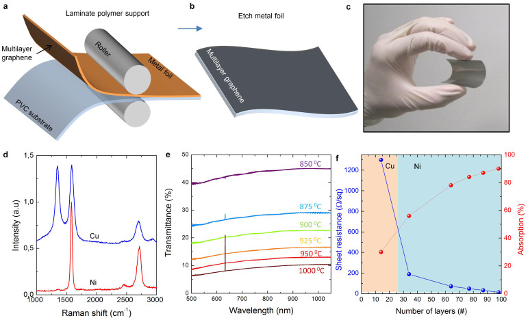
Figure 1a and 1b show the preparation steps of multilayer graphene electrodes on flexible substrates. We synthesized large area multilayer graphene on metal foils using chemical vapor deposition. After the growth, we laminated 75 μm thick polyvinyl chloride (PVC) films at 120°C on the graphene coated side of the foils (Figure 1a). Etching the foils with diluted hydrochloric acid solution yields large area graphene films on transparent and flexible substrate (Figure 1c and Supplementary Information Figure S1). We used copper and nickel foils as a growth substrate in chemical vapor deposition of graphene layers. Figure 1d shows the Raman spectra of graphene samples grown on nickel and copper foils. The multilayer graphene samples grown on copper foils are more defective (intense D-band) than the ones grown on nickel foils. This is because of the different growth mechanisms; the growth mechanism on copper is based on surface adsorption which yields defective multilayer graphene, however, the growth mechanism on nickel is based on precipitation of the dissolved carbon in the foil29. The growth time and the temperature determine the number of graphene layers grown on nickel and copper foils, respectively. We estimated the thickness of the synthesized MLG from the transmittance spectra and measured the sheet resistance of the MLG electrodes using transfer length method (TLM, Supporting information Figure S2). Figure 1e shows the optical transmittance spectra of various samples that have MLG grown on nickel at temperatures from 850 to 1000°C. On copper foils, we were able to grow MLG up to 20 layers, however MLG grown on nickel foils, were much thicker between 30–100 layers. The variation of the sheet resistance and optical absorption with the layer number is given in Figure 1f. The sheet resistance decreases from 1300 to 13 ohm/sq as the number of layers increases from 14 to 98. At the same time optical absorption increases from 30 to 90%. The MLG electrodes on PVC have mechanical flexibility with bending radius down to 2 mm with a constant the sheet resistance (within 1%, Supplementary Information Figure S3).
Figure 1. Synthesis and characterization of multilayer graphene on flexible substrates.
(a), Transfer printing of large area multilayer graphene on flexible PVC substrates by lamination process. Multilayer graphene electrodes were synthesized on metal foils (copper or nickel), then 75 μm thick PVC film was laminated on graphene coated side. (b), Etching the metal foils yields flexible multilayer graphene electrodes on the PVC support. (c), Photograph showing the flexible multilayer graphene electrodes. (d), Raman spectra of the samples synthesized on copper and nickel foils. (e), Optical transmittance spectra of the MLG electrodes using grown on nickel at different temperatures. (f), Variation of the sheet resistance (blue curve) and optical absorption (red curve) of MLG electrodes with the layer number.
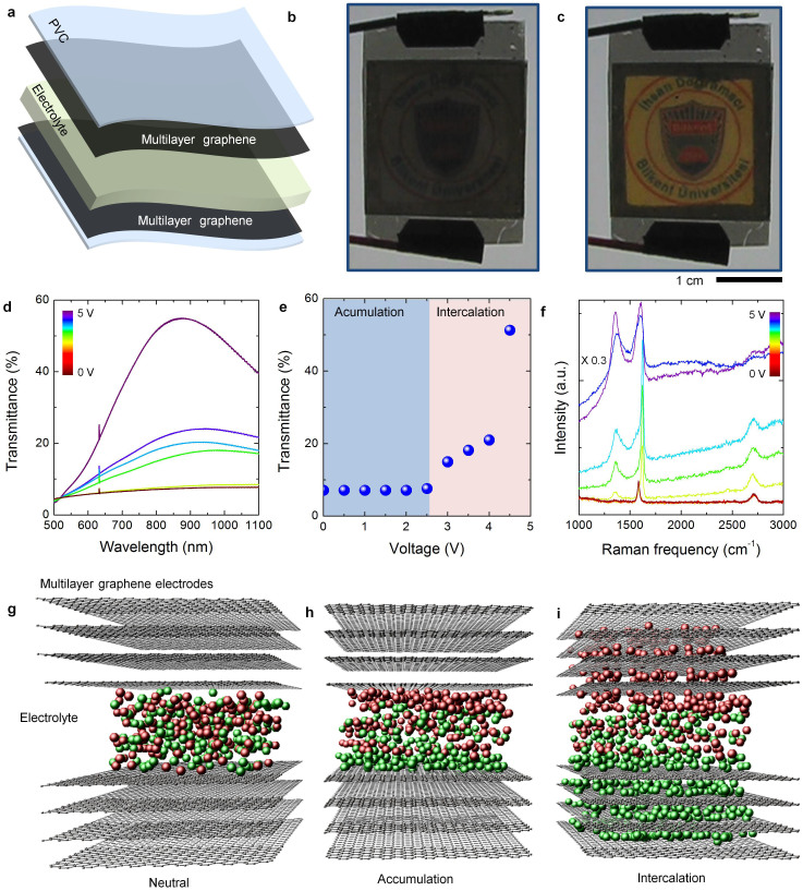
To fabricate the electrochromic devices, we attached two graphene coated PVC substrates with a spacer and filled the gap with an ionic liquid electrolyte. The spacer is a 250 μm thick frame containing 50 μL ionic liquid electrolyte (Diethylmethyl(2-methoxyethyl)ammoniumbis(trifluoromethylsulfonyl)imide). Figure 2a shows the schematic exploded view of the device. We started our investigation by measuring the optical transmittance of the device. For the voltage range from 0 to 2.5 V, we do not observe a significant change in the transmittance however, as we increase the voltage further, the transmittance increases rapidly and the device become more transparent at 5 V (Supporting information Movie 1 and Movie 2). Figure 2b and 2c show the photographs of the device at 0, and 5 V, respectively. We put the logo of our university behind the device with a backlight illumination. At 5 V, the logo appears clearly through the device (Figure 2c). The transmittance spectra under applied voltage from 0 V to 5 V are shown in Figure 2d. At 0 V, the transmittance is only 8% and slightly varies with the wavelength. At 5 V, the transmittance increases sharply to 55% at 900 nm. Figure 2e shows the variation of the transmittance at 800 nm with the applied voltage. The modulation of the spectra originates from the blocking of interband transitions of the graphene layers via electrostatic doping. However, this requires effective doping of underneath layers. Surprisingly, the above layers can be doped when we applied large bias voltages. We propose that the efficient doping of above layers is due to intercalation of ions into the graphene layers. According to our observation, using thicker spacer which contains more ionic liquid (~100 μL) didn't affect the device operation in terms of transmittance modulation or charging time. However using thinner spacer, which contains less volume of ionic liquid, can cause electrical shortage between the top and bottom graphene layers in large scale devices due to the sagging of the flexible substrate.
Figure 2. Graphene electrochromic devices.
(a), Exploded-view illustration of the graphene electrochromic device. The device is formed by attaching two graphene coated PVC substrates face to face and imposing ionic liquid in the gap separating the graphene electrodes. (b,c), Photographs of the devices under applied bias voltages of 0 V and 5 V, respectively. The image of Bilkent University logo [copyright permission from I.D. Bilkent University] appears at 5 V. Demonstrated device is composed of two multilayer graphene electrodes synthesized at 925°C each having ~78 layers. (d), Transmittance spectra of the device under applied voltage between 0 V to 5 V. (e), Variation of the transmittance (at 800 nm) with the applied voltage. (f), Variation of the Raman spectra of graphene electrodes under the applied voltage. (g–i), Schematic representation of the proposed operating regimes, i.e. neutral, charge accumulation, and intercalation, respectively.
To understand the mechanism behind the optical modulation, we measured the Raman spectra of the graphene electrode under the applied voltage (Figure 2f). For applied voltages less than 2.5 V, Raman spectra show no significant change, however, after 2.5 V, the intensity of G-band significantly increases, and D-band appears. Furthermore we observed a strong fluorescence background. The enhancement of G-band and the background fluorescence indicate strong electrostatic doping of graphene layers while appearance of D-band shows formation of defects in graphene layers30. These observations suggest that after a threshold voltage which is around 2.5 V, ions can intercalate into the multilayer graphene through the induced defects and provide effective doping on the above layers. The schematic drawings in Figure 2g–2i demonstrate proposed mechanism for the observed electrochromism. Applied voltage less than 2.5 V, polarizes the ionic liquid and charges accumulate at the graphene-electrolyte interface. We named this range as “accumulation” which results in a very small optical modulation (around 2% of the initial transmittance) due to doping of the graphene layer at the electrolyte interface. Applied voltage larger than 2.5 V induces structural defects and initiates intercalation of ions into the graphene layers (Figure 2i). Appearance of intense D-band in the Raman spectra after 2.5 V indicates the formation of defects on the graphene which enhances the intercalation process. We have tested various electrolytes including water based electrolytes and ionic liquids. The electrochemical window of the electrolyte is a key parameter to achieve effective doping of the graphene layers via intercalation process. We observed that, water based electrolytes do not yield effective intercalation due to narrow electrochemical window. We obtained the best performance with ionic liquid [DEME][TFSI] which has an electrochemical window between −3.0 to 3.5 V.
At the very first cycle, we also observed that color change initiates at the edge and propagates along the device (Supplementary Information Figure S4). The color change of multilayer graphene is reversible and can be cycled many times. Intentionally created structural defects on graphene with the applied voltage has only long term effects on device operation. We showed that the devices are stable for 70 cycles of switching between on and off states. (~50 minutes of continuous operation) (Supplementary Information Figure S6). We also measured a change in the resistance of MLG electrodes. For applied voltages of less than 5 V, the resistance of electrode decreases from 180 to 110 Ω. When MLG is transparent, its resistivity is less than the neutral state. These experiments suggest that the observed electrochromic effect is not because of a chemical reaction that oxidizes the graphene electrodes31,32 but it is because of the intercalation process which electrostatically dopes the graphene layers.
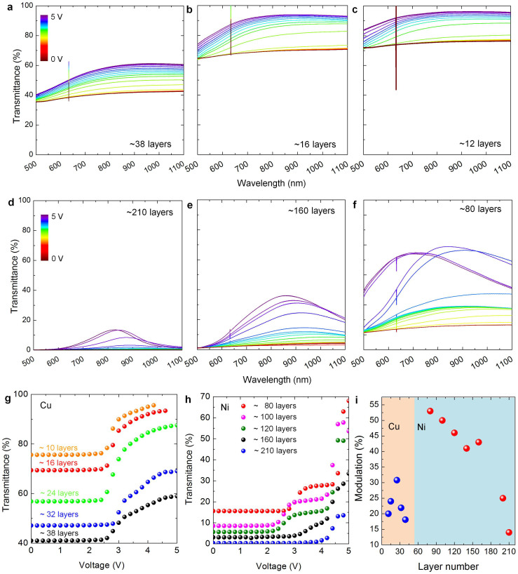
Since the observed optical contrast is defined by the efficiency of the intercalation process, the thickness of MLG determines the device performance. We fabricated a series of devices using MLG with varying thickness. Figure 3a–3f shows the voltage controlled transmittance modulation of 6 representative devices that have MLG electrodes with various thickness. Devices shown in Figure 3a–3c were fabricated by using MLG grown on copper while the devices shown in Figure 3d–3f were fabricated by using MLG grown on nickel foils. The inset shows the estimated number of graphene layers (Supplementary Information Figure S5). Since the graphene quality affects the device operation in terms of transmittance modulation, MLG grown on copper or nickel foils yields some differences in the device performance. Nickel foils produce more crystalline graphene than copper foils. This significantly enhances the device characteristics. For the devices using MLG grown on copper, we observed a flat optical response over a broad spectrum (Figure 3a–3c), however, for the devices using MLG grown on nickel, the modulation spectra show a broad peak centered at 850 nm (Figure 3d–3f). Moreover, we also observed a tradeoff between initial optical absorption (at 0 V) and transmittance modulation efficiency. The thickness of a multilayer graphene electrode defines the maximum transmittance modulation efficiency that the electrochromic device can have. For thin MLG (~20 layers), the optical absorption can be blocked, however for very thick MLG (>50 layers), the intercalation process is inadequate that yields diminishing optical modulation. The variation of the transmittance at 800 nm is plotted in Figure 3g (for the devices using MLG grown on copper foils) and Figure 3h (for the devices using MLG grown on nickel foils). Graphene grown on copper yield less modulation but smooth variation with the applied voltage, however, graphene grown on nickel yield larger modulation with steep variation with the applied voltage. The measured optical modulation is plotted in Figure 3i against the estimated number of graphene layers. Maximum modulation of 30% can be obtained with 25 layers of MLG electrodes grown on copper foil, whereas, MLG grown on nickel foils yield modulation of 55% and decays as the number of graphene layers increases.
Figure 3. Effect of thickness and quality of graphene on the device performance.
(a–f), Transmittance spectra (under applied voltage ranging from 0 V to 5 V) of electrochromic devices using various thicknesses of MLG. Devices shown in (a–c) use MLG grown on copper foils while devices shown in (d–f) use MLG grown on nickel foils, respectively. The inset shows the estimated number of graphene layers. The color bar shows the applied voltage. (g,h) Variation of the transmittance (at 800 nm) of ECD using MLG grown on copper and nickel foils, respectively. (i), Maximum optical modulation plotted against the estimated number of graphene layers.
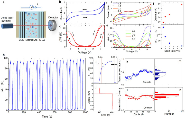
To understand the charging and discharging dynamics of the graphene electrochromic devices, we performed simultaneous electrical and optical characterization. Figure 4a shows the experimental configuration used to measure current-voltage (Figure 4b) and transmittance-voltage (Figure 4c, at 635 nm wavelength) curves. The electrical current and optical transmittance was measured simultaneously, as we swept the voltage between −5 V to 5 V with a scan rate ranging from 0.5 V/sec to 5 V/sec. We observed a profound hysteresis in both current and optical transmittance. The arrows represent the scan direction of the voltage. Interestingly, these devices provide optical bistability. For example, at 4 V bias voltage, the device has two distinct optical transmittance depending on the scan direction. The level of hysteresis varies with the scan rate (Figure 4d and 4e). As we increase the scan rate, the charging current increases (Figure 4f) whereas the optical modulation diminishes sharply (Figure 4g). The hysteresis is a characteristic behavior of supercapacitors due to the formation of electric double layers. We also observed an asymmetry between the charging and discharging cycles. To further characterize charging and discharging time scales, we applied 5 V and 0 V in a sequence and recorded the time trace of the optical transmittance and charging current (Figure 4h). The charging time (3.5 sec) is significantly larger than the discharging time (0.25 sec). This difference is clearly seen in Figure 4i which shows the optical modulation during a single cycle. The current during charging and discharging cycles are also different. When we applied 5 V, the charging current starts from 5 mA and decays exponentially. During the discharging, we measured a current of 20 mA which decays much faster (Figure 4j). This asymmetric behavior is likely due to the variation of the electrical conductivity of the graphene electrodes. In the charged state, the conductivity is larger than its value in the discharged state because of electrostatic doping. In order to test the stability of the device, we measured the time trace of optical transmittance for 70 cycle (Supplementary Information Figure S6) and plotted the histogram of the intensity of the transmitted light at the on- (Figure 4k and 4m) and off-state (Figure 4l and 4n). The variation of the transmittance in the off-state is much less than the variation of the transmittance in the on-state which is likely due to inhomogeneous charging.
Figure 4. Charging and discharging characteristics of graphene electrochromic devices.
(a), Schematic illustration of the experimental setup used for the simultaneous electrical and optical characterization of the graphene electrochromic devices. (b), Current-voltage and (c), transmittance-voltage curves at 635 nm at a scan rate of 0.5 V/s. (d), Current-voltage and (e), transmittance-voltage for different scan rates. (f), Maximum current and (g), maximum optical modulation versus the scan rate. (h), Optical switching characteristics of the device at 635 nm. (i,j) Time variation of transmittance and charging current for a single switching cycle. The extracted RC time constants of the electrochromic device (3.5 seconds for charging and 0.25 seconds for discharging respectively) are illustrated on the single switching cycle with intervals defined by the red bars. (k,l), Long term stability of the transmittance in the on-state (at 5 V) and off-state (0 V). (m,n), The histogram of the transmittance in the on- and off-state.
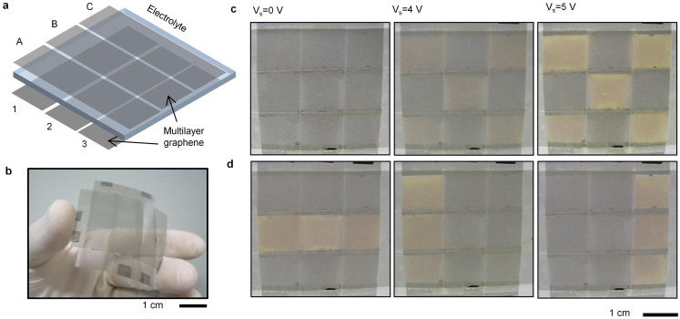
To show the promises of graphene electrochromic devices, we fabricated a multi-pixel flexible electrochromic display. We synthesized large area (5 cm × 5 cm) graphene electrodes and transferred them on a PVC support. The top and bottom graphene layers were patterned to form three 1 cm wide ribbons and placed face to face perpendicularly (Figure 5a). The top and bottom graphene electrodes were separated by a thin spacer to prevent electrical shorting. Figure 5b shows the photograph of the fabricated device. The device is flexible and can be curved with 1 cm radius without any damage on graphene electrodes. We first applied voltage to alternating electrodes to form a chessboard pattern (Supplementary Information Movie 3). We take the snapshots of the device at various voltages (Figure 5c). After 4 V, the chessboard pattern appears clearly. The transmittance of individual pixels can be reconfigured by changing the voltages applied to the rows and columns. Figure 4d represents different patterns obtained at 5 V applied voltage. The performance of the individual pixels is similar to the single pixel devices. The pixel size of the display device can be easily scaled down by photolithography and etching process.
Figure 5. Multi-pixel display device.
(a), Schematic illustration of the multi-pixel display device consisting of 3 × 3 arrays of flexible electrochromic device. (b), Photograph of the fabricated flexible multi-pixel device. (c), Photographs of the device under various bias voltages that generate chessboard pattern. (d), Photographs of the device under 5 V bias voltage with different reconfigurable patterns.
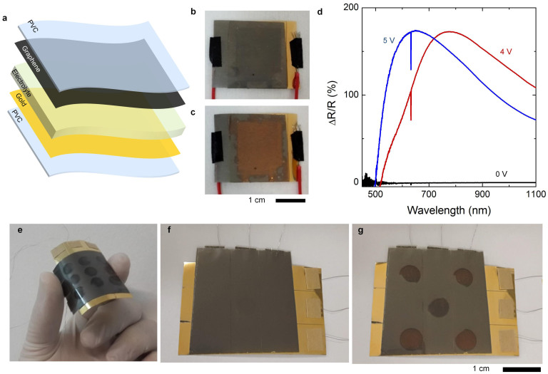
Furthermore, we fabricated reflective type graphene electrochromic devices. This device consists of electrolyte sandwiched between gold and graphene electrodes (Figure 6a). MLG was transferred on a PVC support by lamination process and 100 nm thick gold electrode was evaporated on another PVC support. Figure 6b and 6c show the photograph of the device at 0 and 5 V applied voltages. When the device is unbiased, it looks black due to absorption of the MLG electrodes. Under an applied voltage of 5 V, MLG electrodes become transparent and the color of the device turns into yellow due to underneath gold layer. The reflection spectra at various applied voltages are shown in Figure 6d. This simple device architecture provides new possibilities for reconfigurable mirrors. As an example we fabricated multi-pixel reflective device, by patterning the gold and MLG electrodes (Figure 6e). We isolated the pixels using a spacer with circular holes that contain the ionic liquid. Figure 6f and 6g show the chessboard pattern appearing on the device under 5 V applied voltage. The device is bendable and the pattern is reconfigurable.
Figure 6. Graphene based reflective electrochromic devices.
(a), Exploded-view schematic illustration of the reflective graphene-electrochromic device consisting of gold and multilayer graphene electrodes. (b,c) Photograph of the fabricated device at 0 V and 5 V applied voltage, respectively. (d), Modulation of the reflectance spectra of the devices under various applied voltages. (e), Photograph of the flexible multi-pixel reflective device. (f,g), Photographs of the reflective device under bias voltage of 0 V and 5 V that generate chessboard pattern.
As a conclusion, we demonstrated a new class of flexible electrochromic devices using multilayer graphene electrodes. We show that the optical transmittance of MLG can be controlled by electrostatic doping via reversible intercalation of charges into the graphene layers. Simultaneous electrical and optical characterizations of the graphene electrochromic devices reveal the mechanism behind electrochromic operation. The demonstrated reflective/transmissive multipixel electrochromic display device and reflection type device highlight the promises of the method. The key attributes of our flexible devices are the simplicity of device architecture, high optical contrast and broad band operation. Compatibility with roll-to-roll fabrication processes enables scalable approaches for large area applications. We believe that this work provides a significant step in realization of flexible optoelectronic devices.
Methods
Synthesis of multilayer graphene
Multilayer graphene samples were synthesized on 25 μm thick copper and nickel foils (Alfa Aesar item #13382 and Alfa Aesar item #12722 respectively) by chemical vapor deposition at various temperatures ranging from 850°C to 1000°C at the ambient pressure. H2, Ar and CH4 gases were used during the growth process. CH4 gas served as a carbon feedstock and only sent during the growth. Flow rates of the CH4, H2, and Ar were set as 30 sccm, 100 sccm, 100 sccm respectively. Growth times were 30 min for copper foils and 5 min for nickel foils. After terminating the growth, the samples were left for fast cooling to room temperature. By controlling the growth time and temperature, we obtained series of multilayer graphene samples having various thickness (10 to 250 layers according to the growth temperature.)
Transfer-printing of multilayer graphene
In order to obtain large scale and flexible multilayer graphene electrodes we used lamination technique to transfer the multilayer graphene on transparent PVC substrates. At 120°C, we laminated 75 μm thick PVC film on the graphene coated side of metal foils conformably and etched the foils from back side in %30 hydrochloric acid solution. When the metal foils was completely etched in an hour, the PVC support holding multilayer graphene was rinsed in DI water and left to fast air drying. The multilayer graphene remains stable on the flexible PVC even after bending the substrate.
Preparation of the electrochromic device
After the transfer printing process, we attached two graphene coated PVC substrates using 250 μm thick adhesive frames (Frame-Seal™ - Bio-Rad). The cell is filled with 50 μL ionic liquid electrolyte [DEME][TFSI] (98.5%, Diethylmethyl (2methoxyethyl)ammoniumbis(trifluoromethylsulfonyl)imide, Sigma-Aldrich, 727679. We attached two copper wires to apply voltage to the graphene electrodes using conductive carbon tape.
Optical transmittance measurements
The transmittance measurements were performed by using Bruker Vertex 70 V FTIR spectrometer integrated with Si photodiode. We worked in the wavelength range between 450–1100 nm. We biased the graphene ECD using Keithley 2400 source measure unit during the transmittance measurements. The charging current is also recorded during the measurement.
Raman spectroscopy
Jobin Yvon Horiba Raman microscope system with 50× microscope objectives is used for Raman measurements. The excitation wavelength was 532 nm. The transparent geometry of the electrochromic device allows us to measure the Raman spectrum of the graphene layers under applied bias. During the Raman measurements, the voltage bias was applied by Keithley 2400 source-measure-unit.
Author Contributions
E.O.P. and C.K. planned the experiment; E.O.P. fabricated the samples. E.O.P., C.K. and O.B. performed the experiments. C.K. and E.O.P. analyzed the data and wrote the manuscript. All authors discussed the results and contributed to the scientific interpretation as well as to the writing of the manuscript.
Supplementary Material
Real time movie of the graphene based electrochromic device
Real time movie of the graphene based electrochromic device
Real time movie of the electrochromic display device
Supplementary information for the growth and characterization of the devices
References
- Monk P. M. S., Mortimer R. J. & Rosseinsky D. R. Electrochromism and Electrochromic Devices. Vol. 421. (Cambridge University Press, Cambridge, 2007). [Google Scholar]
- Somani P. R. & Radhakrishnan S. Electrochromic materials and devices: present and future. Mater. Chem. Phys. 77, 117–133 (2003). [Google Scholar]
- Sonmez G. Polymeric electrochromics. Chem. Commun. 42, 5251–5259 (2005). [DOI] [PubMed] [Google Scholar]
- Granqvist C. G. Oxide electrochromics: An introduction to devices and materials. Sol. Energ. Mat. Sol. C 99, 1–13 (2012). [Google Scholar]
- Wang C. J., Shim M. & Guyot-Sionnest P. Electrochromic nanocrystal quantum dots. Science 291, 2390–2392 (2001). [DOI] [PubMed] [Google Scholar]
- Llordes A., Garcia G., Gazquez J. & Milliron D. J. Tunable near-infrared and visible-light transmittance in nanocrystal-in-glass composites. Nature 500, 323–326 (2013). [DOI] [PubMed] [Google Scholar]
- Nikolou M. et al. Dual n- and p-Type Dopable Electrochromic Devices Employing Transparent Carbon Nanotube Electrodes. Chem. Mater. 21, 5539–5547 (2009). [Google Scholar]
- Cho S. I. et al. Nanotube-based ultrafast electrochromic display. Adv Mater 17, 171–175 (2005). [Google Scholar]
- Wang F. H., Itkis M. E., Bekyarova E. & Haddon R. C. Charge-compensated, semiconducting single-walled carbon nanotube thin film as an electrically configurable optical medium. Nat. Photon. 7, 460–466 (2013). [Google Scholar]
- Mortimer R. J. Electrochromic Materials. Annu. Rev. Mater. Res. 41, 241–268 (2011). [Google Scholar]
- Beaujuge P. M., Ellinger S. & Reynolds J. R. The donor-acceptor approach allows a black-to-transmissive switching polymeric electrochrome. Nat. Mater. 7, 795–799 (2008). [DOI] [PubMed] [Google Scholar]
- Granqvist C. R. Electrochromic materials: Out of a niche. Nat. Mater. 5, 89–90 (2006). [DOI] [PubMed] [Google Scholar]
- Gratzel M. Materials science - Ultrafast colour displays. Nature 409, 575–576 (2001). [DOI] [PubMed] [Google Scholar]
- Gan X. T. et al. Chip-integrated ultrafast graphene photodetector with high responsivity. Nat. Photon. 7, 883–887 (2013). [Google Scholar]
- Xia F. N., Mueller T., Lin Y. M., Valdes-Garcia A. & Avouris P. Ultrafast graphene photodetector. Nature Nanotechnol. 4, 839–843 (2009). [DOI] [PubMed] [Google Scholar]
- Lemme M. C. et al. Gate-Activated Photoresponse in a Graphene p-n Junction. Nano Lett. 11, 4134–4137 (2011). [DOI] [PubMed] [Google Scholar]
- Mueller T., Xia F. N. A. & Avouris P. Graphene photodetectors for high-speed optical communications. Nat. Photon. 4, 297–301 (2010). [Google Scholar]
- Gabor N. M. et al. Hot Carrier-Assisted Intrinsic Photoresponse in Graphene. Science 334, 648–652 (2011). [DOI] [PubMed] [Google Scholar]
- Polat E. O. & Kocabas C. Broadband Optical Modulators Based on Graphene Supercapacitors. Nano Lett. 13, 5851–5857 (2013). [DOI] [PubMed] [Google Scholar]
- Zhang X. et al. A graphene-based broadband optical modulator. Nature 474, 64–67 (2011). [DOI] [PubMed] [Google Scholar]
- Novoselov K. S. et al. Electric field effect in atomically thin carbon films. Science 306, 666–669 (2004). [DOI] [PubMed] [Google Scholar]
- Wang F. et al. Gate-variable optical transitions in graphene. Science 320, 206–209 (2008). [DOI] [PubMed] [Google Scholar]
- Nair R. R. et al. Fine structure constant defines visual transparency of graphene. Science 320, 1308–1308 (2008). [DOI] [PubMed] [Google Scholar]
- Kim J. et al. Electrical Control of Optical Plasmon Resonance with Graphene. Nano Lett. 12, 5598–5602 (2012). [DOI] [PubMed] [Google Scholar]
- Majumdar A., Kim J., Vuckovic J. & Wang F. Electrical Control of Silicon Photonic Crystal Cavity by Graphene. Nano Lett. 13, 515–518 (2013). [DOI] [PubMed] [Google Scholar]
- Bonaccorso F., Sun Z., Hasan T. & Ferrari A. C. Graphene photonics and optoelectronics. Nat. Photon. 4, 611–622 (2010). [Google Scholar]
- Liu M., Yin X. B. & Zhang X. Double-Layer Graphene Optical Modulator. Nano Lett. 12, 1482–1485 (2012). [DOI] [PubMed] [Google Scholar]
- Mak K. F., Ju L., Wang F. & Heinz T. F. Optical spectroscopy of graphene: From the far infrared to the ultraviolet. Solid State Commun. 152, 1341–1349 (2012). [Google Scholar]
- Li X. S., Cai W. W., Colombo L. & Ruoff R. S. Evolution of Graphene Growth on Ni and Cu by Carbon Isotope Labeling. Nano Lett. 9, 4268–4272 (2009). [DOI] [PubMed] [Google Scholar]
- Wang F. et al. Controlling inelastic light scattering quantum pathways in graphene. Nature 471, 617–620 (2011). [DOI] [PubMed] [Google Scholar]
- Loh K. P., Bao Q. L., Eda G. & Chhowalla M. Graphene oxide as a chemically tunable platform for optical applications. Nat. Chem. 2, 1015–1024 (2010). [DOI] [PubMed] [Google Scholar]
- Ekiz O. O., Urel M., Guner H., Mizrak A. K. & Dana A. Reversible Electrical Reduction and Oxidation of Graphene Oxide. Acs Nano 5, 2475–2482 (2011). [DOI] [PubMed] [Google Scholar]
Associated Data
This section collects any data citations, data availability statements, or supplementary materials included in this article.
Supplementary Materials
Real time movie of the graphene based electrochromic device
Real time movie of the graphene based electrochromic device
Real time movie of the electrochromic display device
Supplementary information for the growth and characterization of the devices


