Abstract
A compact and robust magnetic label detector for biomedical assays is implemented in 0.18-μm CMOS. Detection relies on the magnetic relaxation signature of a microbead label for improved tolerance to environmental variations and relaxed dynamic range requirement, eliminating the need for baseline calibration and reference sensors. The device includes embedded electromagnets to eliminate external magnets and reduce power dissipation. Correlated double sampling combined with offset servo loops and magnetic field modulation, suppresses the detector offset to sub-μT. Single 4.5-μm magnetic beads are detected in 16 ms with a probability of error <0.1%.
Index Terms: Biosensor, CMOS, magnetic bead, magnetic relaxation
I. Introduction
Magnetic microbeads and nanoparticles have been widely used in biomedical applications, such as cell separation and imaging. Recently, magnetic bead assays have been developed where magnetic beads are used as labels for target analytes [1]–[3]. Unlike the enzymatic labels used predominantly today in solutions such as enzyme-linked immunosorbent assays (ELISA), magnetic labels benefit from negligible background, are chemically stable over a wide temperature range, and do not require complex optical instrumentation that is difficult to miniaturize [4]. By contrast, many techniques are available for detecting magnetic labels, including giant magnetoresistance (GMR) devices [1], superconducting quantum interference devices (SQUID) [2], Hall-effect sensors [3] and inductors [5]. Hall-effect sensors are amenable to integration and scaling of CMOS technology, and hence enable very compact and low cost systems. Magnetically labeled bioassays are therefore a promising approach for addressing the requirements and growing need of point-of-care diagnosis.
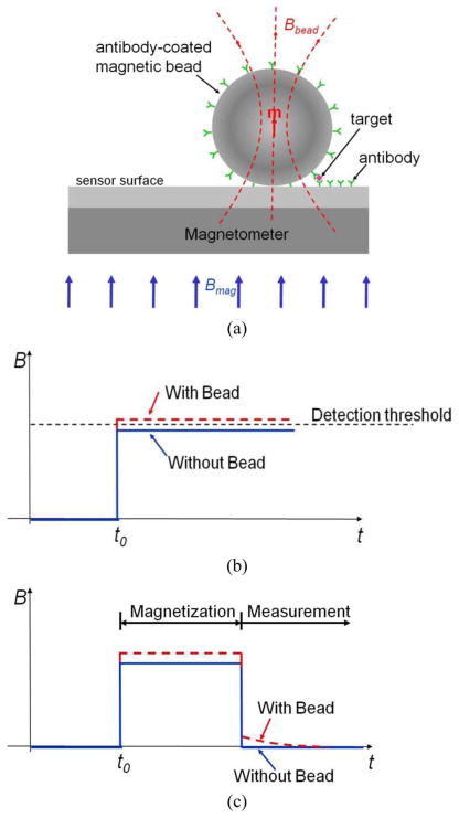
Fig. 1(a) shows the working principle of the magnetic label detection platform. The immobilized target analyte is labeled by a magnetic microbead coated with antibodies specific to the target. Owing to its small size, the label is only magnetic in the presence of an external magnetizing B-field Bmag and decays rapidly when the external field is removed.
Fig. 1.
Magnetic label detection principles and methods. (a) Label detection platform. (b) Conventional magnetization detection method: label detected based on signal difference in magnetization. (c) Relaxation detection method.
Detecting the magnetic field from the bead in the presence of the much larger magnetizing field imposes severe requirements on the detector’s dynamic range, offset, linearity, and temperature stability. For example, a typical 2.8-μm-diameter bead with susceptibility χ = 1 in a 10-mT external field generates less than 20 μT of induced field 10-μm away from the bead center. This induced magnetic field from the bead, Bbead, is more than 50 dB lower than the magnetizing field Bmag (the “baseline”). Previously published bead detection methods attempt to resolve a miniscule change from the bead superimposed on the much larger baseline [see Fig. 1(b)]. Since the baseline is sensitive to environmental variations, these solutions generally require baseline calibration and/or active temperature stabilization.
One approach to overcome this problem is to apply the magnetizing field orthogonal to the sensitive axis of the sensor and detect the fraction of the bead response that is aligned with the sensitive axis [6], [7]. Unfortunately, this solution suffers from several drawbacks. First, it requires precise alignment of the sensor to the magnetizing field. For example, a 60 dB rejection of the magnetizing field requires alignment accuracy better than 0.1 degrees. Moreover, the magnetizing field must be homogeneous, thus requiring a significantly larger magnet and larger power dissipation than integrated solutions with on-chip magnetizing field generation.
Our proposed solution avoids these drawbacks by detecting the magnetic relaxation signature from the label. As shown in Fig. 1(c), the bead is first magnetized by a large field generated on-chip. The measurement starts after this magnetizing field is removed rapidly, thus eliminating the large baseline and detecting the decaying magnetic field from the bead. Prior demonstrations of relaxation field measurements relied on highly sensitive magnetometers such as SQUID and fluxgate sensors [8], [9]. Unfortunately these devices introduce a significant delay between the magnetization and measurement phases, resulting in reduced signal amplitude and increased measurement time.
The solution described here demonstrates a fully integrated magnetic bead detector for biomedical assays that does not require external magnets or baseline calibration and is insensitive to temperature variations. It exploits the short time constants achievable in modern sub-micron CMOS technology to perform relaxation field measurements to reject magnetic interference and device offset. Since the magnetizing field does not need to be homogeneous, it can be generated on chip with appropriate wiring. Thanks to the proximity to the bead and sensor, much smaller magnetizing fields are required, resulting in significantly reduced power dissipation. Aligning the magnetizing field with the sensitive axis of the detector increases the detector output, thus permitting the use of Hall-effect sensors available in standard CMOS technology and eliminating the need for non-standard magnetometers such as GMRs. The entire magnetic label detector, including the electromagnets, the magnetometers and the readout electronics is integrated on a single 2.5 mm × 2.5 mm chip fabricated in a standard 0.18-μm CMOS process.
This paper is organized as follows. Section II describes the principles of magnetic relaxation. Section III discusses the design challenges and the proposed solutions. System architecture and detailed circuit diagram are described in Section IV. In Section V, characterization data of the device for beads with 2.8- and 4.5-μm diameter is presented.
II. Magnetic Relaxation
The magnetic microbeads used in this experiment consist of superparamagnetic iron oxide nanoparticles dispersed in a polymer matrix [10]. When a pulsed magnetizing field is applied, the magnetic dipole moments of the superparamagnetic nanoparticles are first aligned. After the magnetizing field is abruptly switched off, the dipole moments rotate to their easy axis according to the Néel relaxation mechanism, with time constant
| (1) |
where τ0 is approximately 1 ns, T is the temperature in Kelvin, k is the Boltzmann constant and ΔE is the anisotropy energy barrier for the thermal fluctuation to overcome. ΔE depends on the nanoparticle’s volume V and its anisotropy constant K, which is governed by its magnetocrystalline structure and other properties such as shape. The beads used in the experiment presented in this paper have relaxation time constants τN on the order of 300 ns. The intrinsic magnetic properties of nanoparticles can be extracted from relaxation dynamics [9]. Furthermore, various nanoparticles can be differentiated by their relaxation characteristics [11], which could potentially lead to a broader range of applications.
III. Design Challenges
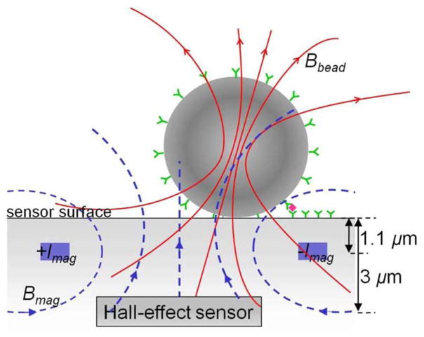
Fig. 2 shows the cross section of a magnetic bead sensor element. A current Imag passing through a pair of metal wires on both sides of the N-Well Hall-effect sensors generates the magnetizing field Bmag. Since in typical multilayer metal processes, the chip surface is as much as 10-μm above the active devices and the magnetic signal from the bead decays with the third power of distance, a simple post-processing step is used to remove the second layer of metal and all the interlayer dielectric (ILD) material above it in the sensor area. The post processing does not require extra masks and can be performed on the wafer level [12]. After post processing, the chip surface is 3-μm from the embedded Hall-effect detectors and 1.1-μm from the current-carrying wires. The limitation to only one layer of metal and polysilicon for interconnects imposes layout challenges that will be discussed in Section IV.
Fig. 2.
Cross section of a CMOS magnetic label detector.
Since the magnetic signal from single microbead is typically ~10 μT, care must be taken to reject interferences from Earth’s magnetic field (~50 μT), time-varying stray magnetic fields from the power line and nearby electrical equipment, and other urban noise. Moreover, the DC offset from the Hall-effect sensors and the CMOS readout circuit is several orders-of-magnitude larger than the signal. The dominant offset arises from miniaturized Hall-effect sensors due to fabrication imperfections such as contact misalignment. The equivalent input-referred sensor offset could be as large as 300 mT, translating into a requirement of more than 90 dB DC offset rejection. Thermo-electric and thermo-magnetic effects on the chip also introduce errors that significantly exceed the small signal from the bead. For instance, the thermopower of silicon is about 0.5 mV/K [13], or equivalently, 8.3 mT/K for the Hall-effect sensors presented in this paper. So a local thermal gradient as little as one degree can result in an error that is three orders-of-magnitude larger than the signal from the bead. Finally, flicker noise from the CMOS electronics and thermal noise from both the sensor and readout circuit must be considered.
We apply several techniques to reduce these errors. First, the magnetizing field is modulated to separate the signal from low frequency noise and DC offset. Second, a mixed-signal servo loop suppresses the sensor offset. Third, correlated double sampling (CDS) is applied to reject low-frequency non-idealities and the thermal effects. The principle is illustrated in Fig. 3. In phase 1, the bead is magnetized for tm with the magnetizing field Bmag. The bead responds with its own magnetic field, Bbead. In phase 2, is Bmag removed rapidly, Bbead decays during tr with a time constant described by (1). In phase 3, the magnetizing field is reversed and relaxation occurs again in phase 4. The net relaxation signal is measured by taking the difference between phases 2 and 4, and then averaged over many cycles to suppress errors due to thermal noise.
Fig. 3.
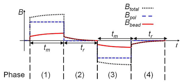
Modulation timing diagram.
IV. System Architecture and Circuit Design
A. System Architecture
Fig. 4 shows the block diagram of the prototype magnetic bead detector chip. Since the micron-sized beads generate only a localized field and therefore cannot be detected by a single sensor with large area, the magnetic sensor is organized into four banks of 64 individual Hall-effect devices. In each bank, the active sensors are surrounded by dummies to minimize sensor-to-sensor variation and thermal non-uniformity. In this prototype, the sensor outputs are processed serially through a multiplexed readout channel that performs offset rejection and signal amplification.
Fig. 4.
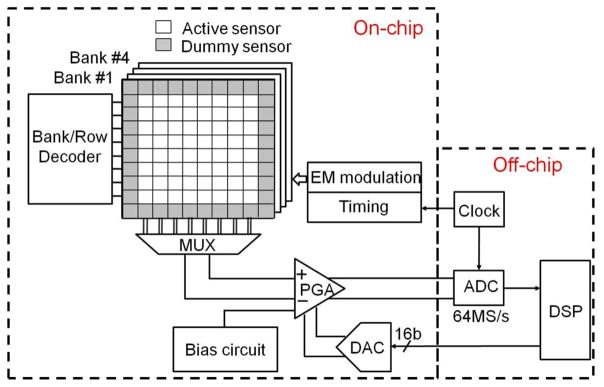
Chip block diagram.
B. Hall-Effect Sensor Element and Array
In standard CMOS processes, Hall plates can be realized either with a diffusion layer (e.g., N-Well) or the channel region of a transistor. In this prototype, N-Well Hall-effect sensors are chosen due to their higher carrier mobility and therefore higher sensitivity [14].
The Hall plate size is optimized based on bead size, signal magnitude and physical design rules. The bead can be modeled as dipole located above the sensor surface which is 3-μm from the embedded sensor as shown in Fig. 2. The induced magnetic field is then
| (2) |
where μ0 is the vacuum permeability, m is the magnetic dipole moment, and r is a vector pointing from the center of the bead to the point where the field is being measured. Since the bead signal decays with the third power of distance |r|, the size of the plate should be minimized. On the other hand, individual Hall plate lateral dimensions must be large compared to the sensing contacts and depth of the N-Well. In the 0.18-μm CMOS technology used in this project, the contacts measure 0.45-μm on the side and the depth of the N-Well is 1.05-μm. In this design, the width and length of the Hall plate are chosen to be 4-μm.
Fig. 5(a) shows the circuit diagram of a sensor element consisting of Hall plate modeled by a four-resistor bridge and two access transistors. The size of the access transistors is 3.2/0.18 μm based on a tradeoff between area and readout noise. Although the stray field from beads landing between sensor elements can be detected by adjacent Hall plates, excessive gaps necessitated by larger access switches would result in reduced signal-to-noise ratio and consequent increased detection error or measurement time. As described earlier, the post-processing steps limit the available interconnects to metal one and polysilicon only. Metal is routed horizontally and used for the wires that carry 32-mA alternating current Imag, sensor bias Vbias, and the row select signal WL [see Fig. 5(b)]. The Hall voltages V+ and V− (“bit lines”) are routed vertically in polysilicon. The resistance of each bit line in the sensor element is 19 Ω. Total noise contribution from bit lines is negligible for an 8 × 8 array but can become significant in larger arrays. Each sensor element occupies a total area of 8.5 μm × 6 μm. Hall plates are biased from a 2-V supply and consume 2.1 mA per sensor. Total thermal noise from the sensor element including the access transistors and Hall plate is 97 nT/Hz1/2.
Fig. 5.
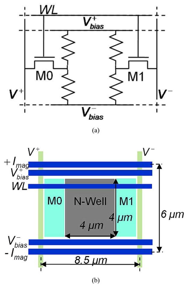
Hall-effect sensor element. (a) Equivalent circuit and (b) layout.
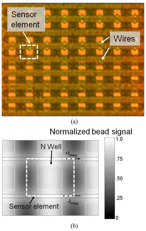
The implementation of an 8 × 8 array is shown in Fig. 6(a). For a magnetic bead assay, it is important to have a large detection area to reduce the measurement uncertainty [15]. Two adjacent rows of sensors share one wire to increase the packing density and thus maximize signal amplitude. Fig. 6(b) shows the total induced Hall voltage by a 4.5-μm bead measured by adjacent sensors as a function of its location. Simulation shows that the bead signal is maximized when the bead is located at the center of the sensor. The worst case occurs when a bead lands between two sensors and the signal is attenuated by about 50% based on simulation and experiment [12].
Fig. 6.
Hall-effect sensor array. (a) Implementation of an 8 × 8 array and (b) total bead signal measured by adjacent sensors versus bead location.
The sensor element can be improved by circuit design techniques and technology change. For instance, the required size of access transistors can be reduced using word-line boosting [16]. Furthermore, since this chip is fabricated in a double-poly process, the sensor surface is farther from the Hall plate than in a single-poly process. Fabrication in a single-poly process would result in increased signal amplitude.
Unlike many other magnetometer devices, Hall-effect sensor will also benefit from technology scaling. Reduced access transistors and Hall plate dimensions, enabled by scaled N-Well thickness, smaller sensing contacts, and thinner metal and ILD, result in higher packing density and increased signal amplitude.
C. On-Chip Electromagnet and Modulation
Each row of sensors is magnetized by an electromagnet implemented with a pair of metal wires carrying 32-mA current in opposite directions. For beads located at the center of sensor surface, the magnetizing field is 2.6-mT at the center of a 2.8-μm bead and 1.8-mT for a 4.5-μm bead, respectively. At the Hall plate the magnetizing field (“baseline”) magnitude is 2.9-mT.
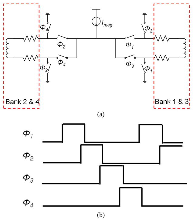
Field modulation is implemented by alternating the current between different wires. Fig. 7(a) shows the schematic of the switching network for one row of sensors in bank 1/3 and bank 2/4. Switches control the direction of the current and the bank to which it is routed. Make-before-break switching, realized by overlapping the switch control signals, keeps the total current constant, thus significantly reducing switching noise. While the total inductance (~120-pH) is negligible at the modulation frequency, the total resistance of the switches and wires must be small so that the current source has sufficient head room to maintain a high output resistance. The resistance for each wire and switch are 20- and 4-Ω, respectively.
Fig. 7.
On-chip electromagnet (a) switch network for one row of sensors and (b) timing diagram.
The timing diagram of the switch network is shown in Fig. 7(b). Note there is a π/2 phase shift between the modulation to bank 1/3 and bank 2/4. When bank 1/3 is in magnetization phase, bank 2/4 is in relaxation phase and vice versa, halving the time required to measure the entire array.
D. Readout Channel
The measured equivalent input-referred DC offset of the miniaturized Hall-effect sensor is 97 mT (1 − sigma value). As discussed in Section III, the offset must be attenuated by more than 90 dB for signal detection. Although sensor offset could be rejected by AC coupling, this would result in a significant area or noise penalty. Conventional Hall-effect sensor offset-cancellation techniques such as spinning-current and orthogonal coupling [17] could not be applied due to significant array area penalty. In our architecture, the offset cancellation is accomplished with the combination of an offset servo loop and CDS.
The offset cancellation in the servo loop is realized by 4-bit calibration DACs in each of the four programmable gain amplifiers (PGAs) that process the sensor output (see Fig. 8). The offset cancellation starts sequentially from the first stage by binary search. The entire offset cancellation process takes less than 8-ms and attenuates the equivalent offset to less than 27-μT. This offset value is independent of applied magnetic field and therefore can be determined even during bioassays when beads are immobilized on sensor surface. Offset cancellation is immediately followed by the relaxation measurement and the sequence is repeated for every sensor.
Fig. 8.
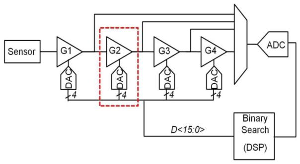
Offset cancellation with the mixed signal loop.
The schematics of one PGA gain stage and 4-bit DAC is shown in Fig. 9. An open-loop gain stage and resistive loads are chosen for their low input-referred noise contribution. The input differential pair is implemented with pMOS transistors to reduce flicker noise. The transconductance of the pMOS is designed to be 4.4 mS so the noise contribution from the PGAs is less than the sensor element. The total input-referred thermal noise and −3 dB bandwidth of the readout electronics is 73 nT/Hz1/2 and 10 MHz, respectively.
Fig. 9.
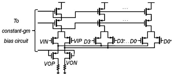
Schematics of one gain stage and DAC (the block highlighted in Fig. 8).
Cascode transistors are used to isolate the output from input and minimize the Miller capacitance. To control the gain variation, the PGA current is set by a constant-gm bias circuit. The gain of each of the first two stages is fixed at 20 dB. The last two stages are source degenerated with total programmable gain up to 37 dB. In each PGA, the DAC is designed to cancel a maximum of 300 mT (or 18 mV) of offset. Each DAC is chosen to be 4-bit so that for every stage the total offset is within the DAC’s range. The PGAs and DACs consume 6.2 mW.
The raw relaxation data after offset cancellation is still overwhelmed by other non-ideal effects such as thermal effects [see Fig. 10(a)]. To reduce the thermal effects, the active sensors are surrounded by dummy sensors and the wires extend well beyond the sensor area. However, due to current modulation, the thermal gradient between the sensing contacts still generates a significant error compared to the signal. For sensors that are close to the edge of the array, this error is measured to be as large as 1.2 mT, which is almost two orders of magnitude of the bead signal. Because in each modulation cycle the current through a wire is turned on/off twice, the thermal effect can be seen as a second harmonic of the modulation frequency f0 = (1)/(2(tm + tr)), and therefore can be filtered by CDS [see Fig. 10(b)] with transfer function
Fig. 10.
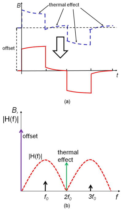
Suppression of offset and thermal effects with CDS. (a) Waveform before (dotted line) and after correlated double sampling (solid line) and (b) frequency response.
| (3) |
Low-frequency non-idealities and the residue DC offset are also attenuated by CDS like a differentiator [18]. After CDS, the relaxation signal is reconstructed. For this prototype, reconstruction is performed by the DSP.
V. Microbead Characterization and Detection
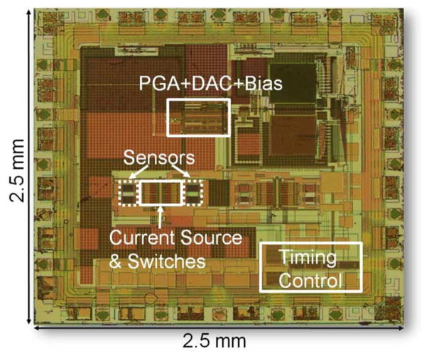
The prototype of microbead detector is implemented in 0.18-μm CMOS and the die photo after post processing is shown in Fig. 11. The sensor banks and electromagnetic modulation block (including the current source and switches) occupy 650 μm × 235 μm. To reduce substrate and power supply coupling, the digital block is kept at one corner of the chip with dedicated power supply. Both the analog and digital blocks operate with 2-V.
Fig. 11.
Die microphotograph.
The microbeads used for the characterization and detection are 4.5- and 2.8-μm in diameters (Dynabeads M450 and M270, Invitrogen, Oslo, Norway). The beads are suspended in de-ionized (DI) water.
A. Sensor Characterization
The Hall-effect sensors are first characterized without beads to make sure that the bead characterization is unaffected by variations of the sensor elements. The sensitivity of all the sensors is measured by a toroid with air gap. The mean voltage-related sensitivity is 0.029/T (or 58 mV/T) with standard deviation less than 2%. This mean sensitivity is used throughout the paper for conversion between magnetic field and voltage.
B. Bead Relaxation Characterization
A two micro-liter droplet with bead is pipetted to the sensor surface and then dried in air. The beads are magnetized for tm = tr = 4 μs. Fig. 12 shows the normalized waveform after CDS. After switching off Bmag at t = 8 μs, the detector response is initially dominated by the readout electronics time constant (~16 ns), and then by the bead relaxation time constant, which is approximately 370 and 300 ns for the M450 and M270 beads, respectively. After turning off Bmag the bead relaxation signal decreases rapidly and after 250 ns is approximately 40 μT (M450) and 18 μT (M270) for beads located near the center of the sensor.
Fig. 12.
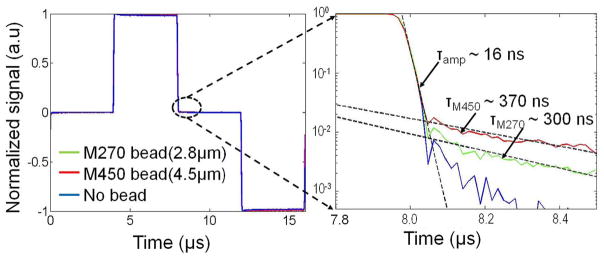
Measured bead relaxation signal.
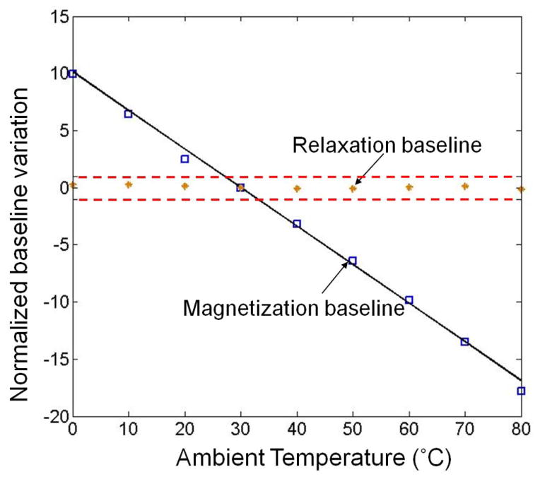
To demonstrate the robustness of the magnetic relaxation detection method, baseline variation is measured and compared for both the conventional magnetization detection method and the relaxation method (see Fig. 13). The ambient temperature is changed from 0 °C to 80 °C. For each detection method, the baseline change is normalized to a 2.8-μm bead signal measured at 30 °C. It is clear that the relaxation baseline variation is negligible compared to the bead signal whereas the magnetization baseline varies more than a 2.8-μm bead signal when the temperature changes by 3 °C. The temperature coefficient of the magnetization baseline is −6.3 × 10⁻³/K or −19 μT/K, which is dominated by Hall mobility variations and close to experimental values reported by other groups [14]. Note that the Hall-effect sensor is not only susceptible to temperature, but also to other environmental factors such as mechanical stress [14]. Therefore, with the magnetization detection method, the baseline must be calibrated carefully to achieve an acceptable detection error. Since this calibration can be performed only when no beads are present near the sensor, it is important that errors remain constant over the course of the measurement. For many biomedical tests incubation of antibodies takes several minutes, this requirement is challenging to meet. The proposed detector avoids this issue.
Fig. 13.
Baseline change versus ambient temperature. The relaxation baseline variation is much smaller than single 2.8-μm bead signal (dotted lines); the magnetization baseline is fitted and its temperature coefficient is 0.33 beads/°C.
C. Bead Detection
The probability of detection error for the presence (“1”) and absence (“0”) of the bead is determined by
| (4) |
where SNR is the signal-to-noise ratio in dB.
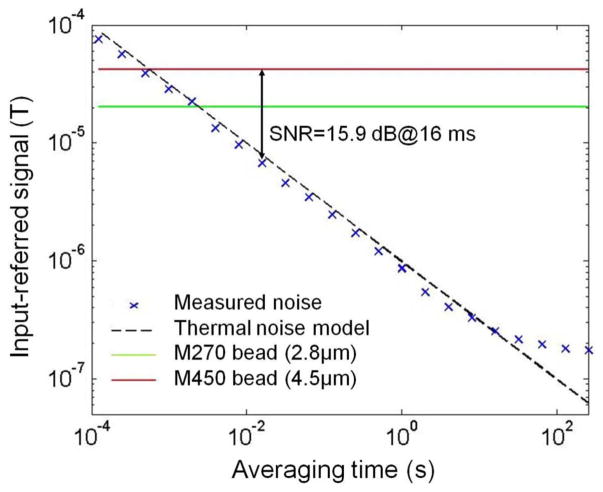
The input-referred noise is measured and shown in Fig. 14. Since the flicker noise is suppressed by CDS, the measured noise is dominated by thermal noise up to 10 seconds of averaging time. The measured signal from a 4.5- and 2.8-μm bead is shown on the same graph. The SNR therefore can be calculated to be 15.9 dB for a 4.5-μm bead when the measurement time is 16 ms. According to (4), this corresponds to a probability of detection error less than 0.1%. It is important to note that the bead signal used here is for the best case when the bead is near the center of the sensor. When a bead is located between two sensors, SNR drops by 9 dB [12] and the measurement time needs to be increased by eight times to maintain the same probability of detection error.
Fig. 14.
Measurement of signal-to-noise ratio.
To demonstrate the feasibility of magnetic label detection for biomedical assays, a 2-μl droplet of diluted M-450 bead sample (40 000 beads/μl) is added on the chip and air dried. The outputs from a 64-sensor array are shown in Fig. 15. The excellent correlation between the optical and the electronic readouts demonstrates the feasibility of robust on-chip detection of single magnetic labels using magnetic relaxation and potential applications in high-sensitivity biomedical assays. When the bead sample is dried, the meniscus force drags some beads to the edge of the sensor array window and causes them to clump. Compared to other label detection platforms, this detector adds extra value by monitoring label distribution with micron resolution and providing real-time assay status. As discussed in Section IV, the imaging resolution will improve with technology scaling.
Fig. 15.
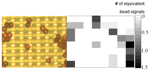
Sensor readouts versus optical image. Left: sensor array photograph with beads; right: corresponding electrical signal.
The performance of the microbead label detector is summarized in Table I. The total power dissipation is dominated by the on-chip electromagnet, which however consumes much less power than external magnets. The total input-referred noise is dominated by the sensor element.
TABLE I.
Chip Performance Summary
| Technology | 0.18 μm CMOS 2P6M |
| Area | 2.5×2.5 mm2 (Chip) |
| 8.5×6 μm2 (Sensor element) | |
| Power | 64 mW (Electromagnet) |
| 4.2 mW (Sensor element) | |
| 6.2 mW (PGA+DAC) | |
| Sensitivity | 0.03/T (Sensor element) |
| Input-referred noise | 97 nT/Hz1/2 (Sensor element) |
| 73 nT/Hz1/2 (PGA+DAC) | |
| Readout channel bandwidth | 10 MHz |
| Input-referred offset | <1 μT |
| Probability of detection error | 0.1% in 16 ms for 4.5 μm bead |
VI. Conclusion
A chip for evaluating biomedical assays labeled with magnetic microbeads is presented. The label detection is based on measuring the magnetic relaxation signature from beads. Compared to conventional magnetization detection methods, this approach significantly reduces sensitivity to environmental variations such as temperature and eliminates the need for individual sensor’s baseline calibration. On-chip current loops are used to magnetize the beads, thus eliminating the need for an external magnet. This reduces overall system power dissipation from Watts to milliwatts, meeting the requirements of portable applications. The Hall-effect sensors used are compatible with standard CMOS technology, greatly reducing cost compared to other solutions using GMRs that require specialized processes. Robust, compact, low-power and low-cost magnetic label detection based on Néel relaxation is suitable for point-of-care biomedical applications.
Acknowledgments
The authors would like to thank the Berkeley Sensor and Actuator Center (BSAC) and the University of California, Berkeley Microlab facility for device post processing.
This work was supported in part by the trans-NIH Genes, Environment and Health Initiative, Biological Response Indicators of Environmental Systems Center under Grant U54 ES016115-01.
Biographies

Paul Peng Liu (S’07) received the B.S. degree in microelectronics from Peking University, Beijing, China, and the M.S. degree in electrical engineering from North Carolina State University, Raleigh. He is currently pursuing the Ph.D. degree in electrical engineering from the University of California, Berkeley.
Prior to joining Berkeley in 2007, he was a Staff Design Engineer with Xilinx Inc., San Jose, CA, where he worked on high-speed serial link transceiver. His current research interests include CMOS/MEMS sensor and analog/mixed-signal integrated circuit design.

Karl Skucha received the B.S. and M.S. degrees in electrical engineering from University of California, Berkeley, in 2006 and 2009, respectively, where he is currently pursuing the Ph.D. degree in electrical engineering with a minor in management of technology.
He is an Intel Robert Noyce fellow and his doctoral work is focused on CMOS-integrated magnetic particle detectors for diagnostic applications.

Yida Duan (S’07) was born in Beijing, China. He received the B.S. degree in electrical engineering and computer science from University of California, Berkeley, in 2007, where he is currently pursuing the Ph.D. degree in electrical engineering and computer science at Berkeley Wireless Research Center.
From May 2010 to August 2010, he was with the Analog Circuit Group, NXP Semiconductors Corporation, San Jose, CA, as a design intern, developing low power SAR ADC. His research interests include power efficient analog digital interface circuits.
Mr. Duan was a recipient of the ADI Outstanding Student Design Award in 2009.

Mischa Megens received the Ph.D. degree in physics from the Van der Waals-Zeeman Institute, University of Amsterdam, The Netherlands, in 1999.
In 2001 he joined Philips Research, where he worked in such diverse fields as biosensors for point-of-care diagnostics, GaN photonic crystal LED light extraction, soft imprint lithography, polymer OLEDs, electrowetting-based beam steering, and ultrasound for cardiac ablation monitoring. He is currently a Senior Research Scientist with University of California, Berkeley, where he is working on high speed optical beam steering using phased arrays of lightweight high contrast grating mirrors.

Jungkyu Kim received the Ph.D. degree in biomedical engineering from the University of Utah, Salt Lake City, in 2009.
He is currently a Postdoctoral Researcher with the Department of Chemistry and Bioengineering, University of California, Berkeley. He has been working in the area of cell/tissue engineering, microfluidic sample processing, nucleic acid sample preparation and on-chip amplification, protein microarray, CNT biosensor and magnetic bead labeled immunoassay.
Dr. Kim was honored with numerous awards, including the Korea Research Foundation (KRF) fellowship, Pierre Lassonde Center fellowship, and the Best Paper Award from the Korea Orthopedic Research Society (KORS).

Igor I. Izyumin (S’05) received the B.S. degrees in electrical engineering and computer science from the University of Missouri, Rolla, in 2008. He is currently pursuing the Ph.D. degree in electrical engineering at the University of California, Berkeley.
Between 2005 and 2006, he was with Adtran, Inc., Huntsville, AL, where he was involved with the development of mixed-signal ASICs. His research interests include MEMS sensor interfaces and mixed-signal integrated circuit design.

Simone Gambini (M’09) received the Laurea Specialistica degree from University of Pisa and Sant’Anna School of Advanced Studies, Pisa, Italy, in 2004, and the Ph.D. degree from University of California, Berkeley, in 2009, all in electrical engineering.
Since January 2011, he returned to U.C. Berkeley as a member of the Berkeley Sensor and Actuator Center to conduct research on CMOS-compatible bio-sensors and MEMS interfaces and to serve as a lecturer in analog circuit design. His doctoral research, developed at the Berkeley Wireless Research Center, was concerned with the design of an ultra-low power radio for sensor networks and was partially funded by an Intel Fellowship. In 2010, he was with Telegent Systems, where he designed RF circuits for highly integrated mobile TV tuners. His research interests include the application of low-power electronics to create microsystems integrating sensing and communication, and the development of circuit design techniques for post-CMOS devices.

Bernhard Boser (F’03) received the Ph.D. degree from Stanford University, Stanford, CA, in 1988.
He was a Member of Technical Staff Bell Laboratories. In 1992, he joined the faculty of the Electrical Engineering and Computer Science Department, University of California, Berkeley. His research interests include the area of analog and mixed signal circuits, with special emphasis on ADCs and micromechanical sensors and actuators.
Dr. Boser has served on the program committees of ISSCC, VLSI Symposium, Transducers, is President of the Solid-State Circuits Society, and a Fellow of the IEEE. He is a co-founder of SiTime, a fabless semiconductor company.
Contributor Information
Paul Peng Liu, Email: pl@eecs.berkeley.edu.
Bernhard Boser, Email: boser@eecs.berkeley.edu.
References
- 1.Baselt DR, Lee GU, Natesan M, Metzger SW, Sheehan PE, Colton RJ. A biosensor based on magnetoresistance technology. Biosens Bioelectron. 1998;13:731–739. doi: 10.1016/s0956-5663(98)00037-2. [DOI] [PubMed] [Google Scholar]
- 2.Chemla YR, Grossman HL, Poon Y, McDermott R, Stevens R, Alper MD, Clarke J. Ultrasensitive magnetic biosensor for homogeneous immunoassay. Proc Nat Acad Sci. 2000;97:14268–14272. doi: 10.1073/pnas.97.26.14268. [DOI] [PMC free article] [PubMed] [Google Scholar]
- 3.Aytur T, Foley J, Anwar M, Boser B, Harris E, Beatty PR. A novel magnetic bead bioassay platform using a microchip-based sensor for infectious disease diagnosis. J Immunol Meth. 2006;314:21–29. doi: 10.1016/j.jim.2006.05.006. [DOI] [PubMed] [Google Scholar]
- 4.Myers F, Lee L. Innovations in optical microfluidic technologies for point-of-care diagnostics. Lab Chip. 2008;8:2015–2031. doi: 10.1039/b812343h. [DOI] [PubMed] [Google Scholar]
- 5.Wang H, Chen Y, Hassibi A, Scherer A, Hajimiri A. A frequency-shift CMOS magnetic biosensor array with single-bead sensitivity and no external magnet. IEEE ISSCC Dig Tech Papers. 2009:438–439. [Google Scholar]
- 6.Li G, Sun S, Wilson RJ, White RL, Pourmand N, Wang SX. Spin valve sensors for ultrasensitive detection of superparamagnetic nanoparticles for biological applications. Sens Actuators A. 2006;126:98–106. doi: 10.1016/j.sna.2005.10.001. [DOI] [PMC free article] [PubMed] [Google Scholar]
- 7.Besse PA, Boero G, Demierre M, Pott V, Popovic R. Detection of a single magnetic microbead using a miniaturized silicon Hall sensor. Appl Phys Lett. 2002;80:4199–4201. [Google Scholar]
- 8.Eberbeck D, Hartwig S, Steinhoff U, Trahms L. Description of the magnetisation decay in ferrofluids with a narrow particle size. Magnetohydrodyn. 2003;39:77–83. [Google Scholar]
- 9.Ludwig F, Heim E, Schilling M. Characterization of superparamagnetic nanoparticles by analyzing the magnetization and relaxation dynamics using fluxgate magnetometers. J Appl Phys. 2007 Jun;101–10:113909-1–113909-10. [Google Scholar]
- 10.Fonnum G, Johansson C, Molteberg A, Morup S, Aksnes E. Characterization of Dynabeads® by magnetization measurements and Mössbauer spectroscopy. J Magn Magn Mater. 2005;295:41–47. [Google Scholar]
- 11.Liu P, Skucha K, Megens M, Boser B. A CMOS Hall-effect sensor for the characterization and detection of mangetic nanoparticles for biomedical applications. IEEE Trans Magn. 2011 Oct;47:3449–3451. doi: 10.1109/TMAG.2011.2158600. [DOI] [PMC free article] [PubMed] [Google Scholar]
- 12.Skucha K, Liu P, Megens M, Kim J, Boser B. A compact Hall-effect sensor array for the detection and imaging of single magnetic beads in biomedical assays. Dig. 16th Int. Conf. Solid-State Sensors Actuators; 2011; pp. 1833–1836. [Google Scholar]
- 13.Geballe T, Hull G. Seebeck effect in silicon. Phys Rev. 1955;98:940–947. [Google Scholar]
- 14.Popovic RS. Hall Effect Devices. 2. New York: IOP; 1991. [Google Scholar]
- 15.Hassibi A, Zahedi S, Navid R, Dutton RW, Lee TH. Biological shot-noise and quantum-limited SNR in affinity-based biosensor. J Appl Phys. 2005;97:084701–9. [Google Scholar]
- 16.Ishibashi K, Takasugi K, Yamanaka T, Hashimoto T, Sasaki K. A 1-V TFT-load SRAM using a two-step word-voltage method. IEEE J Solid-State Circuits. 1992 Nov;27(11):1519–1524. [Google Scholar]
- 17.Maupin JT, Geske ML. The Hall Effect and Its Applications. New York: Plenum; 1980. The Hall effect in silicon circuits; pp. 421–445. [Google Scholar]
- 18.Enz C, Temes G. Circuit techniques for reducing the effects of Op-Amp imperfections: Autozeroing, correlated double sampling and chopper stabilization. Proc IEEE. 1996 Nov;84(11):1584–1614. [Google Scholar]


