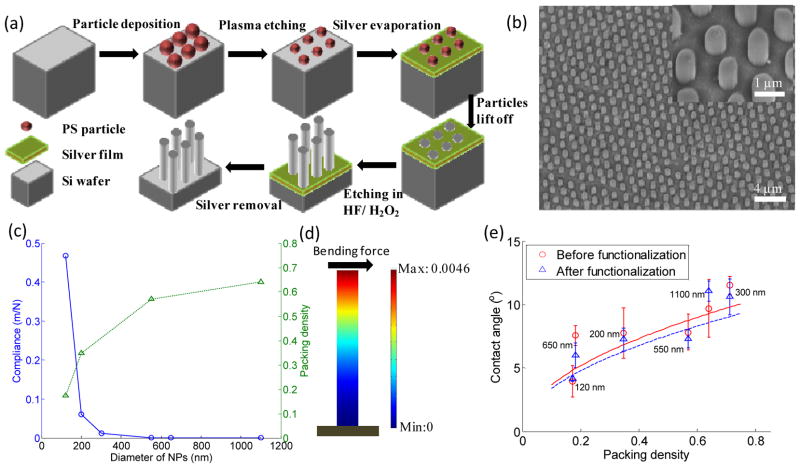
Fig. 1.
(a) Fabrication process of NP arrays by metal assisted chemical etching method. (b) A typical SEM image of NP arrays with average diameter of 650 nm from tilted view. The inset in (b) shows the magnification of NPs from tilted view. (c) Mechanical and geometrical properties of NP substrates: compliance and packing density. (d) A finite element method (FEM) analysis of a single bending NP showing the displacement of an NP with diameter of 120 nm. The unit of the color bar is nanometer. (e) Wettability of different NP substrates before and after functionalization. The solid line and dashed line stand for fitted curves using Cassie's law for non-functionalized and functionalized NP substrates, respectively. Error bars in (e) stand for standard derivation from three independent experiments.

