Abstract
A flat microdevice which incorporates a thin-film amorphous silicon (a-Si:H) photodetector with an upper layer of functionalized SiO2 is used to quantify the density of both immobilized and hybridized DNA oligonucleotides labeled with a fluorophore. The device is based on the photoconductivity of hydrogenated amorphous silicon in a coplanar electrode configuration. Excitation, with near UV/blue light, of a single-stranded DNA molecule tagged with the fluorophore 1-(3-(succinimidyloxycarbonyl)benzyl)-4-(5-(4-methoxyphenyl)oxazol-2-yl) pyridinium bromide (PyMPO), results in the emission of visible light. The emitted light is then converted into an electrical signal in the photodetector, thus allowing the optoelectronic detection of the DNA molecules. The detection limit of the present device is of the order of 1 × 10¹² molecules/cm2 and is limited by the efficiency of the filtering of the excitation light. A surface density of 33.5 ± 4.0 pmol/cm2 was measured for DNA covalently immobilized to the functionalized SiO2 thin film and a surface density of 3.7 ± 1.5 pmol/cm2 was measured for the complementary DNA hybridized to the bound DNA. The detection concept explored can enable on-chip electronic data acquisition, improving both the speed and the reliability of DNA microarrays.
INTRODUCTION
DNA chips are revolutionizing the acquisition and analysis of genetic information (1–6). In the case of massively parallel microarrays, DNA target sequences are analyzed by promoting hybridization with different capture single-strand DNA ‘probes’ immobilized at specific sites in the microarray. The quantification of the hybridization event that takes place at each site in the microarray is mostly based on labels (colorimetric, chemiluminescent, radioactive or fluorescent) that are previously bound to the DNA target molecules. Upon hybridization with the DNA probe immobilized in the array, a detection system [e.g laser scanners, charged-couple device (CCD) cameras] must be used to quantify the amount of labeled DNA target. The detection limits associated with these methodologies range from 1 to 600 fmol/cm2 (7). Label-free detection systems that are based on the physicochemical changes that occur upon binding of probes and targets have also been used. Examples include surface plasmon resonance and piezoelectric devices in quartz crystal microbalances (8,9).
The most used optical detection systems rely on fluorescence microscopy to capture the emission of fluorescence labels (10–12). Although fluorescence detection systems are extremely sensitive, they require very expensive, complex and large external optical systems to acquire and analyze the biological data. An on-chip electronic data acquisition system would improve both the speed and the reliability of DNA chip hybridization pattern analysis. A further advantage would be a lower cost for the DNA microarray analysis, particularly in the case of portable hand-held instruments for applications such as point-of-care diagnostics.
Thin film microelectronics is a microfabrication technology based on hydrogenated amorphous silicon (a-Si:H), which has been used mostly to fabricate thin-film transistors in matrix-addressed arrays for flat-panel displays and light sensors for photoreceptors and solar cells [for a review of a-Si:H see Street (13)]. Webster et al. (14) have described the use of silicon-based PIN photodiodes with on-chip interference filters integrated onto electrophoresis columns for detecting fluorescence signals of double-stranded DNA fragments.
The low temperature processing (T < 400°C) characteristic of thin film technology allows the use of a wide variety of substrates such as glass (large area and low cost), plastic (flexible and low cost) and biocompatible materials. This flexibility potentially enables the chemical activation of surfaces and the creation of biocompatible environments for DNA immobilization and hybridization (15,16).
In the present work, thin film microelectronics technology is used to create a DNA chip platform with an integrated electronic detection system. The innovative structure proposed and described integrates a functionalized SiO2 thin-film flat surface with a thin-film, multi-layered, photodetector based on a-Si:H. The top functionalized SiO2 layer is used to covalently immobilize DNA probes that can further hybridize with complementary DNA targets labeled with a fluorophore. The photodetector lying beneath the surface SiO2 layer is then used to optoelectronically quantify the light emitted by the labeled DNA molecules. Barrier and filter layers are included in the photodetector structure in order to improve the sensitivity of the device. This optoelectronic detector structure can become the basis for the design of an array of optoelectronic detectors enabling rapid, reliable and inexpensive on-chip detection of series of parallel occurring DNA hybridization events.
MATERIALS AND METHODS
Chemicals
All chemicals and solvents were purchased from Sigma (Spain), or Merck (Portugal), unless stated otherwise, and used without additional purification. The end-modified DNA oligonucleotides used as probes and targets were from ThermoHybaid (Germany). The silanization reagent 3-aminopropyltriethoxysilane (APTES) was purchased from Sigma and the hetero-bifunctional cross-linker sulpho succinimidyl 6-maleimidylhexanoate (sulfo-EMCS) was from Pierce (USA). The fluorescent dye 1-(3-(succinimidyloxycarbonyl)benzyl)-4-(5-(4-methoxyphenyl)oxazol-2-yl) pyridinium bromide (PyMPO) was from Molecular Probes (USA). Bovine serum albumin (BSA) and sodium dodecyl-sulfate (SDS) were from Sigma.
DNA probes and targets
Seventeen base-pair long oligonucleotides modified at the 5′-end with a thiol group (-SH) and with an amine (-NH2) group at the 3′ end, and with the following base sequence were used as DNA probes: HS-5′-TTAACTTTGTTAAAAAC-3′-C7-NH2. DNA targets used as positive and negative controls were also 17 bp long but modified only at the 5′-end with an NH2 group. The following sequences were used for the complementary and non-complementary target respectively: NH2-5′-GTTTTTAACAAAGTTAA-3′ and NH2-5′-ACA CGGTCCAGACTCCTACG-3′.
Photodetector concept
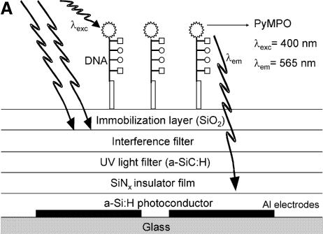
The detection concept is based on the photoconductivity of a-Si:H in a coplanar electrode configuration (Fig. 1A). Hydrogenated amorphous silicon is a photoconductive, direct bandgap, thin-film semiconductor with an optical bandgap Eg ∼1.7 eV (12). The onset of interband absorption leads to a peak in spectral response between 500 and 600 nm. Below 500 nm the spectral response decreases due to surface recombination losses. Selected optical and electronic properties of the a-Si:H thin-films are described in Table 1. The fluorescent dye PyMPO was chosen as the label because: (i) it has a large Stoke’s shift (λexcitation = 400 nm; λemission = 560 nm); (ii) its emission wavelength is at the peak of the a-Si:H spectral response; and (iii) it can be chemically attached to the amine termination of DNA probes. The objective is to detect the presence of the PyMPO-labeled DNA by an increase in the photocurrent in the a-Si:H layer.
Figure 1.
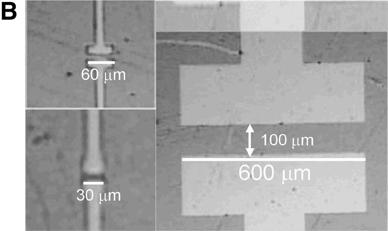
(A) Schematic diagram of the DNA chip surface with integrated photodetector for the quantification of tagged DNA molecules. (B) Optical microscope images of three photodetectors with different aluminum parallel contact lengths (and contact separation distances): 30 µm (5 µm), 60 µm (10 µm) and 600 µm (100 µm).
Table 1. Properties of a-Si:H thin-film used as photodetector.
| Tauc optical bandgap, Eopt | 1.7 eV |
|---|---|
| Intrinsic conductivity at RT, σdi | 10–10 S cm–1 |
| Activation energy of σdi | 0.9 eV |
| Photoconductivity (G = 1021 cm–3s–1) | 10–4 S cm–1 |
| Electron drift mobility, µe | 1 (cm2V–1s–1) |
| Hole drift mobility, µh | 10–3 (cm2V–1s–1) |
| Electron lifetime, τ | 10–7 s |
| n-doped conductivity at RT, σdn | 10–3 S cm–1 |
| p-doped conductivity at RT, σdp | 10–5 S cm–1 |
Device fabrication
The device (Fig. 1A) is fabricated on a glass substrate. The length of the aluminum parallel contacts varies between 30 µm and 3 mm and their separation between 5 and 500 µm (Fig. 1B). The Al metal lines are defined by photolithography in a cleanroom environment. The a-Si:H, silicon nitride (SiNx), amorphous silicon-carbon (a-SiC:H) and silicon dioxide (SiO2) thin-films are deposited by RF-PECVD at temperatures between 200 and 250°C. The SiO2 film is functionalized by a silanization and cross-linking process (see below) and becomes an active layer upon which DNA probes can be covalently immobilized and made available for further hybridization with DNA targets.
DNA labeling and purification
The DNA probes and targets were labeled at the NH2-terminated 3′ end and at the 5′-aminated end respectively, using the fluorescent dye PyMPO. The labeling reaction was performed for at least 6 h. Ethanol precipitation and gel filtration were used to remove the excess of PyMPO molecules according to the manufacturer’s instructions (Molecular Probes, USA). The DNA concentration was quantified by measuring the absorbance of the purified labeled DNA solution at 260 nm.
Surface functionalization
The surface of the SiO2 layer is first cleaned with cholic acid 2% (w/v) for 12 h at room temperature. The surfaces are then silanized with 2% (v/v) APTES in acetone, for 2 h at room temperature (15). This process results in a surface covered with reactive primary amines (-NH2). These NH2 groups are further functionalized by covalently attaching the hetero-bifunctional cross-linker, sulfo-EMCS 1 mM, for 2 h at room temperature.
DNA immobilization and hybridization
After cross-linking, the functionalized SiO2 surface is exposed to an aqueous 0.5 µM DNA probe solution for 3 h at 37°C. The labeled probes are covalently linked to the maleimide termination of the crosslinker monolayer on the chip via the thiol group (13). Afterwards, the samples are washed with 0.1% (w/v) Tween 20 and rinsed thoroughly with de-ionized water. Tests for non-specific immobilization are made by using a single-strand DNA probe (ssDNA) without the thiol termination at the 5′-end. For DNA hybridization experiments, unlabeled DNA probes are first immobilized onto the SiO2 layer functionalized with APTES and modified with sulfo-EMCS as described above. The unreacted sulfo-EMCS maleimide groups are then blocked by exposing the surface of the device for 2 h to a pre-hybridization solution containing 2% (w/v) BSA (17). Hybridization is then carried out overnight at room temperature using a 0.5 µM PyMPO-labeled DNA target solution with 2% (w/v) BSA. Next, the chip is washed twice for 5 min with a solution of 0.5× SSC buffer (7.5 mM Na citrate, pH 7 containing 25 mM NaCl) + 0.1% (w/v) SDS, followed by a thorough rinse with de-ionized water.
The immobilization and hybridization results presented are the average of three repetitions of the same experiment and the error bars represent the standard deviation observed on this average.
Spectral response measurements
One of the parallel Al electrodes is connected to a voltage source and the other to a lock-in amplifier. The incident light (380–800 nm) is chopped at a low frequency (∼13 Hz) and is normal to the a-Si:H detector. The normalized spectral response (SR) is the ratio of the photocurrent to the incident light intensity normalized to its peak. The incident light used has a photon flux of ∼1014 photons.cm–2.s–1 at 400 nm.
Optoelectronic DNA calibration curve
The calibration of the a-Si:H-based photodetector is made by measuring the SR for different surface densities of DNA molecules on the device. Briefly, a specific volume of a PyMPO-labeled DNA solution of known concentration is placed over the entire area between the photodetector electrodes and allowed to dry on air. The surface density of the deposited DNA is calculated by dividing the amount of DNA added by the area of the fluorescent spot formed. After measurement of the photocurrent at that particular DNA surface density, the adsorbed DNA is removed by washing and the spectral response is measured again to confirm that the detector returns to the initial state. This procedure is performed starting with the lowest concentration and is repeated on the same detector for solutions with increasing concentration of PyMPO-labeled DNA probes. The calibration curve is obtained by plotting the spectral response of the a-Si:H-based biodetector at 400 nm (λexc of PyMPO) (after subtraction of the baseline signal) as a function of the DNA surface density (pmol/cm2).
The amount of DNA immobilized or hybridized on the surface of the device can be estimated by measuring the spectral response at 400 nm and converting the value obtained to pmol/cm2 with the calibration curve constructed.
Detectors operating in the photoconductive mode can have gain if the recombination lifetime is larger than the transit time of the majority carrier through the device (18). In our configuration, however, this is not the case as the recombination lifetime (free charge carrier lifetime) is of the order of 10–7 s and the transit time was estimated to be ∼10–4 s. Another factor which might have affected the calibration of the detector response is the dependence of photoconductivity, σph, on the photocarrier generation rate, G, in the a-Si:H, which is known to follow a power law dependence, σph∝Gγ, where γ is between 0.5–1. However, at the low illumination intensities used in this experiment, γ is nearly 1, so the assumption of a linear relationship between the light intensity from PyMPO emission and the detector photocurrent should be valid.
Fluorescence DNA calibration curve
PyMPO-labeled capture probes were diluted in de-ionized water in a dilution series ranging from 0.1 to 20 µM DNA. A known volume of each standard solution was spotted in triplicates on glass slides and allowed to dry. The fluorescent intensity of each spot was measured with a fluorescence microscope (Olympus CX40). Fluorescence images were digitized and the emitted fluorescence signal was quantified with commercial image processing software to obtain a standard curve for the DNA probe. Similar calibration curves for the PyMPO-labeled target DNA were made using dilutions between 0.05 and 10 µM. After immobilization or hybridization on the thin-film chip, the fluorescence signal measured by microscopy was used to calculate the amount of DNA from the corresponding calibration curves.
RESULTS AND DISCUSSION
Incorporation of barrier and filter layers
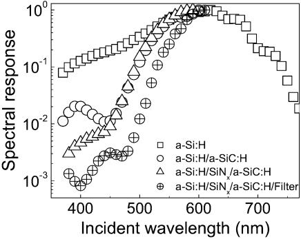
Since the a-Si:H layer has a significant photosensitivity in the UV, a UV filter consisting of an a-SiC:H (Eg = 2.1 eV) layer was deposited above the a-Si:H photoconductor to lower its absorption of light at the PyMPO excitation wavelength. This increased the sensitivity of the device by one order of magnitude (Fig. 2, circles). It is estimated that the PyMPO absorbs about 0.4% of the light at 400 nm. A thin SiNx layer was used to reduce the spill-over of photogenerated carriers in the a-SiC:H into the a-Si:H. By adding the SiNx and a-SiC:H layers on top of the initial a-Si:H photodetector, the ratio between the device response at 560 and 400 nm increased from 3, for the initial a-Si:H single layer device (Fig. 2, squares) to 700 (Fig. 2, triangles).
Figure 2.
Improvement of the sensitivity of the photodetector at 400 nm (λexc of PyMPO) by successively adding an a-SiC:H UV light filter layer, a SiNx carrier barrier layer and an interference filter. The spectral response curves were normalized to the highest signal.
To further increase the sensitivity of the device at 400 nm, an interference filter composed of a high-refractive-index quarter wave layer, followed by a multilayer of 15 bilayers of (λ/4) of SiOx (n = 1.57; d = 637 Å)/SiNx (n = 1.89; d = 529 Å) was fabricated. This filter reflects 95% of the light at 400 nm. The use of this type of filter above the detector/barrier/a-SiC:H filter stack increases the detector sensitivity by three orders of magnitude (Fig. 2, crossed circles). It is estimated that the filter stack allows ∼60% of the light emitted by the PyMPO at 560 nm to reach the a-Si:H photodetector.
Improvements in the sensitivity of the a-Si:H photodetector device will require the development of a more effective filter to the UV light. High quality, precision bandpass interference filters can allow a rejection by a factor of 103 to 104 relative to the peak transmittance. This would allow the signal of the present device in the blue region to be decreased further by 3–4 orders of magnitude and would allow detection levels comparable to the presently used fluorescence techniques (e.g. laser scanning, CCD camera).
DNA calibration curve
Measurement of the SR curve of the detector in the presence of PyMPO shows an increase in the detector signal in the 400–450 nm range. This occurs because PyMPO, when excited at this wavelength, emits light with a spectrum centered in the visible (λem = 565 nm), which is in turn absorbed by the a-Si:H photoconductor, resulting in a photocurrent. Because the detector has an integrated UV filter, the overall effect of the system in the presence of UV illumination is an apparent increase in the response at 400–450 nm when PyMPO, or DNA labeled with PyMPO, is present on the surface. A system of filters, integrated in the chip between the a-Si:H photodetector and the SiO2 layer upon which the DNA probes are immobilized, serves to block the UV/blue excitation light while allowing the emitted light at 565 nm to be transmitted to the a-Si:H layer, producing a photoresponse. Thus, tagging DNA molecules with the dye PyMPO allows the use of an a-Si:H photodetector to optoelectronically detect the presence of DNA and to quantify the amount of labeled DNA present. To improve the signal to noise ratio of the device, it is crucial that the photoresponse of the sensor be as low as possible in the 400–450 nm excitation range.
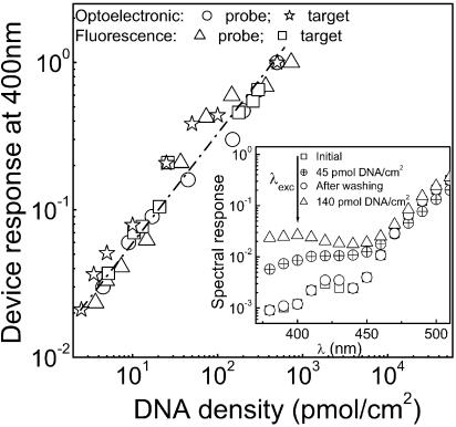
In order to construct the DNA calibration curve, different amounts of DNA probes and targets labeled with PyMPO were adsorbed onto the optimized photodetector and the corresponding responses at 400 nm were measured. After washing away the probes, the spectral response of the a-Si:H photodetector returns to the initial state (Fig. 3, inset). The normalized response of the device at 400 nm is plotted in Figure 3 for different concentrations of adsorbed DNA probe and target. Figure 3 shows that the detection limit of the present device is ∼2 pmol/cm2.
Figure 3.
Photodetector calibration. The correlation between the photodetector normalized response at 400 nm and the surface densities of the DNA probe and target is shown. Calibration data obtained independently by fluorescence microscopy is shown for comparison. A linear fit between the response device (y) and the spotted DNA density (X) is given by the equation: y = 2.00 × 10⁻³ × X + 8.21 × 10⁻². The inset shows how the initial spectral response of the bio-detector can be restored after measuring 45 pmol/cm2 of DNA labeled with PyMPO by washing the DNA from the device, and how it responds again to 140 pmol/cm2 of DNA labeled with PyMPO.
Calibration curves, using fluorescence microscopy as the detection method, were independently obtained for both DNA probe and target single-strand sequences (as described above). Figure 3 shows that both the optoelectronic and fluorescence calibration curves have the same linear trend for the range of DNA surface densities studied.
Immobilized DNA density
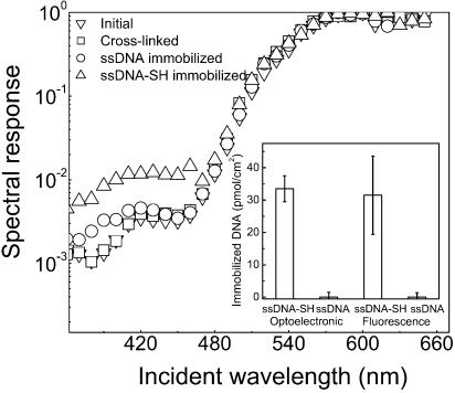
The photodetector was used to quantify the surface density of DNA probes covalently immobilized on the functionalized film deposited over the detector layers. Figure 4 shows that when labeled DNA is immobilized on the silanized SiO2 surface, there is an increase in the device response around 400 nm. Combining this response with the optoelectronic calibration curve of the DNA probe (Fig. 3, open circles), the immobilized DNA density is estimated to be 33.5 ± 4.0 pmol/cm2. A comparable value is obtained when the DNA density is determined by fluorescence microscopy (31.5 ± 12.1 pmol/cm2). This surface density falls within the typical 1–200 pmol/cm2 range reported in the literature for DNA immobilized on functionalized glass and SiO2 surfaces (19–21).
Figure 4.
Normalized spectral response of the photodetector in its initial state, after silanization and crosslinking, after DNA immobilization with DNA containing the specific -SH termination that allows immobilization (ss-DNA-SH), and after exposure to DNA with the same base sequence without -SH termination (ss-DNA). The inset displays the signal obtained using the bio-detector and, independently, by fluorescence microscopy after immobilization of probes with and without the reactive thiol group.
A linear, single stranded, DNA molecule orientated perpendicularly to a surface can be assumed to occupy a cylindrical region in space with a diameter close to the diameter of a B DNA double helix (≈20 Å). Thus, an estimation of the theoretical coverage of a closely packed full monolayer of probes yields 53 pmol/cm2. The density of the immobilized 5′-thiolated DNA probes reported above is typical of a high probe density regime (10). It corresponds to about 63% of this theoretical full DNA monolayer coverage, and to ∼4% of the silanols believed to be present in a clean SiO2 surface (22).
The 5′-end specificity of the DNA probe upon immobilization to the surface was confirmed by repeating the immobilization experiment under the same experimental conditions, but using a DNA probe devoid of the thiol group at the 5′-end. Figure 4 shows that a significant optoelectronic and fluorescence signal is detected only if probes are thiolated at the 5′-end. This result confirms that DNA probes are immobilized on the chip surface only through the 5′-end of the probe and discards any other immobilization mechanism such as adsorption as responsible for the increase in detector signal.
DNA hybridization density
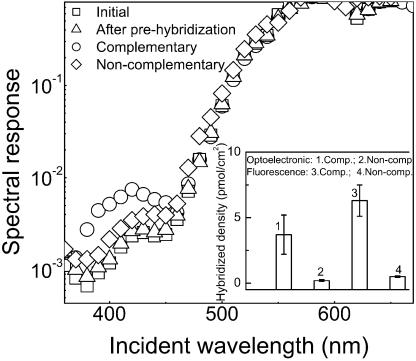
The preparation of surfaces with bound DNA probes in microarrays should guarantee that (i) DNA targets could easily access the probes and (ii) that the hybridization event is selective enough to enable discrimination between fully complementary and non-complementary targets. These concerns were addressed in the current biochip structure by comparing the level of hybridization attained with complementary and non-complementary DNA targets. First, unlabeled DNA capture probes were immobilized on the surface above the photodetector/filter system. Subsequently, non-complementary (negative control) and complementary (positive control) PyMPO-labeled DNA targets were incubated at the surface as described above and the optoelectronic (at 400 nm) and fluorescence responses were recorded. The results are shown in Figure 5.
Figure 5.
Normalized spectral response of the bio-detector in its initial state (with immobilized untagged ssDNA), after pre-hybridization with BSA, and after hybridization of complementary and non-complementary ssDNA targets. The inset shows the signals obtained using the bio-detector and, independently, by fluorescence microscopy after hybridization with a complementary and a non-complementary DNA target.
Hybridization with a complementary DNA target resulted in an increase in the photodetector signal at 400 nm, while non-complementary DNA targets yielded a negligible increase in signal. The density of the hybridized DNA determined with the photodetector was 3.7 ± 1.5 pmol/cm2 and 0.20 ± 0.07 pmol/cm2 for the positive and negative controls, respectively. These densities are in agreement with the values obtained by fluorescence microscopy for hybridization with complementary (6.3 ± 1.5 pmol/cm2) and non-complementary (0.50 ± 0.075 pmol/cm2) DNA sequences. The values obtained with the positive control are also in good agreement with data reported in the literature for DNA hybridization on silanized surfaces (11,18). A comparison of the surface densities determined for the immobilized and hybridized DNA show that ∼11% of the covalently attached probes participate in the formation of a double helix with the targets (hybridization efficiency). This low hybridization efficiency is typical of high probe density regimes (11).
Conclusions
A DNA chip structure that integrates a functionalized SiO2 thin-film flat surface with a thin-film, multi-layered, optoelectronic detector based on a-Si:H was developed for the immobilization and hybridization of DNA. The device, which relies on the labeling of DNA molecules with the fluorophore PyMPO, can detect surface concentrations down to 2 × 10¹² molecules/cm2. A linear detection behavior in the range of 2.5–700 pmol DNA/cm2 was observed. DNA probes were covalently immobilized on the chip surface via a thiol group and a surface density of 33.5 ± 4.0 pmol/cm2 was measured with the integrated photodetector. Furthermore, the hybridization of complementary DNA targets with immobilized and unlabeled DNA probes was successfully photodetected at a surface density of 3.7 ± 1.5 pmol/cm2.
The integrated DNA chip described in this paper presents important advantages over other optical systems: (i) there is no need for expensive and complex equipment for data acquisition and analysis; (ii) on-chip electronic data acquisition can be easily implemented; and (iii) the speed and the reliability of DNA chip hybridization pattern analysis can be improved. This detection system could form the basis of an optoelectronic detector array for the rapid, reliable and inexpensive detection of nucleic acids in a wide variety of DNA microarray applications. It points toward faster, reliable and less expensive biological data acquisition and can allow the use of DNA chips for clinical point-of-care.
Acknowledgments
ACKNOWLEDGEMENTS
The authors gratefully acknowledge F. Silva for help in some of the deposition steps. This work was supported by the Portuguese Ministry of Science and Technology (POCTI/BIO/34022/2000 and Ph.D. grant BD/SFRH/3001/2000 to F. F.).
REFERENCES
- 1.Schena M., Shalon,D., Davis,R.W. and Brown,P.O. (1995) Quantitative monitoring of gene expression patterns with a complementary DNA microarray. Science, 270, 467–470. [DOI] [PubMed] [Google Scholar]
- 2.Duggan D.J., Bittner,M., Chen,Y., Meltzer,P. and Trent,J. (1999) Expression profiling using cDNA microarrays. Nature Genet., 21, 10–14. [DOI] [PubMed] [Google Scholar]
- 3.Xiang C.C. and Chen,Y. (2000) cDNA microarray technology and its applications. Biotechnol Adv., 18, 35–46. [DOI] [PubMed] [Google Scholar]
- 4.Marshall A. and Hodgson,J. (1998) DNA chips: an array of possibilities. Nature Biotechnol., 16, 27–31. [DOI] [PubMed] [Google Scholar]
- 5.Ramsay G. (1998) DNA chips: state-of-the art. Nature Biotechnol., 16, 40–44. [DOI] [PubMed] [Google Scholar]
- 6.Southern E., Mir,K. and Shchepinov,M. (1999) Molecular interactions on microarrays. Nature Genet., 21, 5–9. [DOI] [PubMed] [Google Scholar]
- 7.Ostroff R.M., Hopkins,D., Haeberli,A.B., Baouchi,W. and Polisky,B. (1999) Thin film biosensor for rapid visual detection of nucleic acid targets. Clin. Chem., 45, 1659–1664. [PubMed] [Google Scholar]
- 8.Ng J.H. and Ilag,L.L. (2003) Biochips beyond DNA: technologies and applications. Biotechnol. Ann. Rev., 9, 1. [DOI] [PubMed] [Google Scholar]
- 9.Pividori M.I., Merkoçi,A. and Alegret,S. (2000) Electrochemical genosensor design: immobilisation of oligonucleotides onto transducer surfaces and detection methods. Biosens. Bioelectron., 15, 291–303. [DOI] [PubMed] [Google Scholar]
- 10.Lamture J.B., Beattie,K.L., Burke,B.E., Eggers,M.D., Ehrlich,D.J., Fowler,R., Hollis,M.A., Kosicki,B.B. Reich,R.K. and Smith,S.R. (1994) Direct detection of nucleic acid hybridization on the surface of a charge coupled device. Nucleic Acids Res., 22, 2121–2125. [DOI] [PMC free article] [PubMed] [Google Scholar]
- 11.Peterson Q.W., Heaton,R.J. and Georgiadis,R.M. (2001) The effect of surface probe density on DNA hybridization. Nucleic Acids Res., 29, 5163–5168. [DOI] [PMC free article] [PubMed] [Google Scholar]
- 12.Wang J. (2000) From DNA biosensors to gene chips. Nucleic Acids Res., 28, 3011–3016. [DOI] [PMC free article] [PubMed] [Google Scholar]
- 13.Street R.A. (1991) Hydrogenated Amorphous Silicon. Cambridge University Press, Cambridge, UK. [Google Scholar]
- 14.Webster J.R., Burns,M.A., Burke,D.T. and Mastrangelo,C.H. (2001) Monolithic capillary electrophoresis device with integrated fluorescence detector. Anal. Chem., 73, 1622–1626. [DOI] [PubMed] [Google Scholar]
- 15.Fixe F., Faber,A., Gonçalves,D., Prazeres,D.M.F., Cabeça,R., Chu,V., Ferreira,G. and Conde,J.P. (2002) Thin film micro arrays with immobilized DNA for hybridization analysis. Mat. Res. Soc. Symp. Proc., 723, O2.3.1. [Google Scholar]
- 16.Fixe F., Cabeça,R., Prazeres,D.M.F., Ferreira,G.N.M., Chu,V. and Conde,J.P. (2003) Electric Field Pulse Assisted Covalent Immobilization of DNA in the Nanosecond Time Scale. App. Physics Lett., 83, 1465–1467. [Google Scholar]
- 17.Okamoto T., Suzuki,T. and Yamamoto,N. (2000) Microarray fabrication with covalent attachment of DNA using bubble jet technology. Nature Biotechnol., 18, 438–441. [DOI] [PubMed] [Google Scholar]
- 18.Rose A., (1978) Concepts in photoconductivity and allied problems. John Wiley & Sons, New York, NY, USA. [Google Scholar]
- 19.Rogers Y.H., Jiang-Baucom,P., Huang,Z., Bogdanov,V., Anderson,S. and Boyce-Jacino,M.T. (1999) Immobilization of oligonucleotides onto a glass support via disulfide bonds: a method for preparation of DNA microarrays. Anal. Biochem., 266, 23–30. [DOI] [PubMed] [Google Scholar]
- 20.Beier M. and Hoheisel,J. (1999) Versatile derivatisation of solid support media for covalent bonding on DNA-microchips. Nucleic Acids Res., 27, 1970–1977. [DOI] [PMC free article] [PubMed] [Google Scholar]
- 21.Chan V., Graves,D.J. and McKenzie,S.E. (1995) The biophysics of DNA hybridization with immobilized oligonucleotide probes. Biophys. J., 69, 2243–2255. [DOI] [PMC free article] [PubMed] [Google Scholar]
- 22.Zhuravlev L.T. (1987) Concentration of hydroxyl groups on the surface of amorphous silicas. Langmuir, 3, 316–318. [Google Scholar]


