Abstract
Surface enhanced Raman spectroscopy (SERS) has been widely investigated as an effective technique for low-concentration bio-chemical molecules detection. A rapid two-step approach to fabricate SERS substrates with high controllability in ambient air is developed. Dynamic laser ablation directly creates microgroove on the Si substrate. Meanwhile, nanoparticles are synthesized via the nucleation of laser induced plasma species and the air molecules. It configures the Si surface into four different regions decorated with nanoparticles at different sizes. With Ag film coating, these nanoparticles function as hotspots for SERS. Microsquare arrays are fabricated on the Si surface as large-area SERS substrates by the laser ablation in horizontal and vertical directions. In each microsquare, it exhibits quasi-3D structures with randomly arranged and different shaped nanoparticles aggregated in more than one layer. With Ag film deposition, uniform SERS signals are obtained by detecting the 4-methylbenzenethiol molecules. The SERS signal intensity is determined by the size and shape distributions of the nanoparticles, which depend on the laser processing parameters. With the optimal laser fluence, the SERS signals show a uniform enhancement factor up to 5.5 × 10⁶. This provides a high-speed and low-cost method to produce SERS substrates over a large area.
Raman scattering is an important method to obtain vibrational spectroscopic information of target molecules by the inelastic scattering of photons when they interact with the molecules or atoms1. However, the applications of Raman scattering is limited by intrinsically weak signals due to the small Raman scattering cross-sections of molecules2. Surface enhanced Raman scattering (SERS) provides a desirable solution to enhance the Raman scattering via two primary mechanisms, which can be explained by either electromagnetic theory or chemical theory1,2,3. The electromagnetic theory attributes the enhanced Raman scattering to the electromagnetic field enhancement, which is generated by the excitation of localized surface plasmon resonance (LSPR)3,4. The field enhancement magnifies the intensity of incident light as well as the excited Raman scattered light, leading to a significant increase of the total signal output. On the other hand, the chemical theory attributes the signal enhancement to the charge transfer between the chemisorbed species and the metal surface. In the present work, rough metal surface achieved by Ag thin film coating on laser ablated Si is investigated to enhance the Raman scattering primarily via the electromagnetic mechanism.
Since its discovery in 1977, SERS has provided huge capabilities to fingerprint molecules’ detections and analyses1,2,3,4,5. Despite the continuous achievements in the greater enhancement factors of SERS for ultra-sensitive detection, poor reliability and reproducibility of substrates with large-scale uniformity have severely limited its applications3,4,6. Metallic nanoparticles, deposited on solid substrates, have been widely studied via chemical synthesis and self-assembly7. Such substrates can exhibit large SERS enhancement factors6,7,8. However, the difficulties in controlling signal homogeneity and particle stability prevent its extensive applications for a large-area detection9. To address this issue, SERS substrates have been developed by surface nanopatterning. The frequently used methods are focused ion beam and electron-beam lithography, which allow the precise control of the size and shape of the surface nanostructures and thus achieve high reproducibility of the SERS substrates3,4. The main disadvantages of these techniques are their high cost and slow throughput for large-area SERS substrate fabrication. More recently, 3 dimensional (3D) metallic nanostructures are achieved by various approaches, such as particle mediated aggregation, reactive ion etching and physical vapor deposition10,11,12,13,14. The main purpose is to improve the signal enhancement as well as the uniformity and reproducibility.
Laser irradiation is a versatile method to fabricate micro/nano-structures at a high speed. It provides good solutions to fabricate SERS substrates over a large area9,15. Eric Mazur et al. demonstrated SERS substrates with Ag coated nano-bumps by using femtosecond laser irradiation and then the thermal deposition of Ag thin films. An enhancement factor of 107 was achieved9. Hai-Lung Tsai et al. also demonstrated a one-step method to fabricate SERS substrates by femtosecond laser processing in aqueous silver nitrate solutions16. However, the femtosecond laser processing of the SERS substrates is high-photon-cost and time-consuming to make nanostructures over a large area.
In this paper, a new technique is developed to fabricate large-area Si-based micro/nano-structured SERS substrates in ambient air. The laser scanning along horizontal and vertical directions forms plenty of microsquares. Their boundaries are microgrooves formed by laser ablation deposited with nanoparticles. In the center area of the microsquares, it exhibit quasi-3D structures with randomly arranged and different shaped nanoparticles aggregated in more than one layer. With the Ag thin film deposition, the microsquare regions exhibit uniform enhancement factors (EFs) of approximately 5.5 × 10⁶ at an excitation wavelength of 532 nm. The decoration of nanoparticles is highly dependent on the laser processing parameters during the laser ablation. The size and shape distributions of nanoparticles can be flexibly tuned by varying laser processing parameters to achieve the optimal SERS performance.
Results and discussion
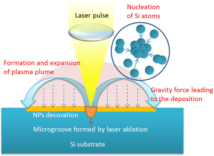
Nanosecond pulsed laser ablation in ambient air is a complicated and explosive process to remove substrate materials and synthesize nanoparticles17. It includes the formation of plasma species, the generation of shock wave, the expansion of plasma plume and the dynamic growth of nanoparticles18. The dynamics of materials’ ejection and nucleation are crucial for the nanoparticles’ generation19. Figure 1 shows the pulsed laser ablation for nanoparticles’ generation. When laser pulses provide high enough fluences, laser irradiation on Si surface can induce the materials’ breakdown and the plasma formation20. The plasma plume is at high pressure and high temperature state20. It consists of laser induced energetic species including atoms, clusters, and particulates21. These plasma species are ejected out from the Si surface anisotropically during the laser ablation and they exhibit high initial kinetic energy due to the strong recoil pressure generated during the plasma formation. The strong interaction between the plasma species and the air molecules promotes the nucleation of the species, which allows the formation and aggregation of nanoparticles20,21. The formed nanoparticles gradually release the kinetic energy by the collisions with the background species during their transport18. The nanoparticles are then deposited onto the Si surface due to the gravity force acting on them. It should be noted that the laser ablation of Si in air leads to the oxidation. An EDX measurement has been done to show the surface materials’ constitutions of flat Si surface and the substrates fabricated at different laser fluences as shown in Table 1. It also suggests that the higher laser fluence during laser ablation leads to a stronger oxidation. The oxidation of Si does not influence the SERS performance because it only depends on the rough metal surface after Ag film coating.
Figure 1. Pulsed laser ablation dynamics for micro/nano-structures’ generation and their deposition on the silicon substrate due to the gravity force.
Table 1. Composition determined using EDX of flat Si surface and the substrates fabricated at different laser fluences.
| Substrates | Atomic % of Si | Atomic % of O |
|---|---|---|
| Flat Si surface | 100 | 0 |
| Laser textured Si surface (Laser fluence: 14.3 J/cm2) | 92.19 | 7.81 |
| Laser textured Si surface (Laser fluence: 21.0 J/cm2) | 72.25 | 27.75 |
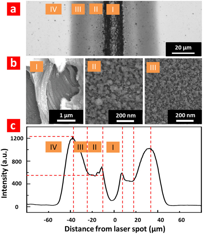
The microscope image of a single line formed by laser beam on the silicon substrate is shown in Figure 2(a). The nanosecond pulsed laser ablation configures the Si surface into four different geometry regions as shown in Figure 2(b). The Si surface in region I includes hybrid micro/nano-structures consisted of the microgroove decorated with nanoparticles. Region II is the Si surface near the microgroove with large size nanoparticles’ (from 50 nm to 200 nm) decoration. In region III, the Si nanoparticles at smaller sizes (less than 50 nm) are observed. Region IV is far away (>60 μm) from the laser ablated microgroove. There is no nanoparticle deposited on the Si surface.
Figure 2.
(a) Microscope image of a single line laser beam scanning (τ = 10 ns, PRR = 100 kHz, laser spot size ~ 20 μm, ν = 100 mm/s and laser fluence15.9 J/cm2) on Si surface and (b) SEM images of regions I, II and III as marked in (a).(c) The average SERS intensity of 1073 cm−1 Raman band (2-naphthylamine molecules’ adsorption) along transverse direction of the single line laser scanning.
The surface morphologies of the different regions can result in various SERS behaviors. After 40 nm Ag film deposition and monolayer 2-naphthylamine adsorption, the SERS signals of the probing molecules are measured. The average SERS intensity of the 1073 cm−1 peak along the transverse direction of the laser scanning is shown in Figure 2(c). It can be seen that the SERS signal is weak (~100 counts) in region I even though there are abundant hybrid micro/nano-structures. This is because the microgroove is tens of microns deep, which makes the SERS signals being limited inside the microgroove and can hardly be detected. The enhanced SERS signal is obtained in the flat Si surface regions II and III. In these regions, hotspots are created by the aggregation of the Ag coated nanoparticles. The size distribution of the nanoparticles greatly influences the SERS performance. The aggregation of the smaller nanoparticles leads to abundant nanogaps and nanocavities, which form the higher density of hotspots with a more intense local field. Therefore, the SERS signal increases with the distance away from the microgroove due to the decrease of the nanoparticles’ size. The maximum SERS intensity reaches to ~1200 counts in region III, which is almost twice higher than that in region II. The SERS performance is weak in region IV. There are very few nanoparticles being deposited in this area. Ag film deposition on the flat Si surface has a much weaker effect on the SERS signal due to the lack of hotspots.
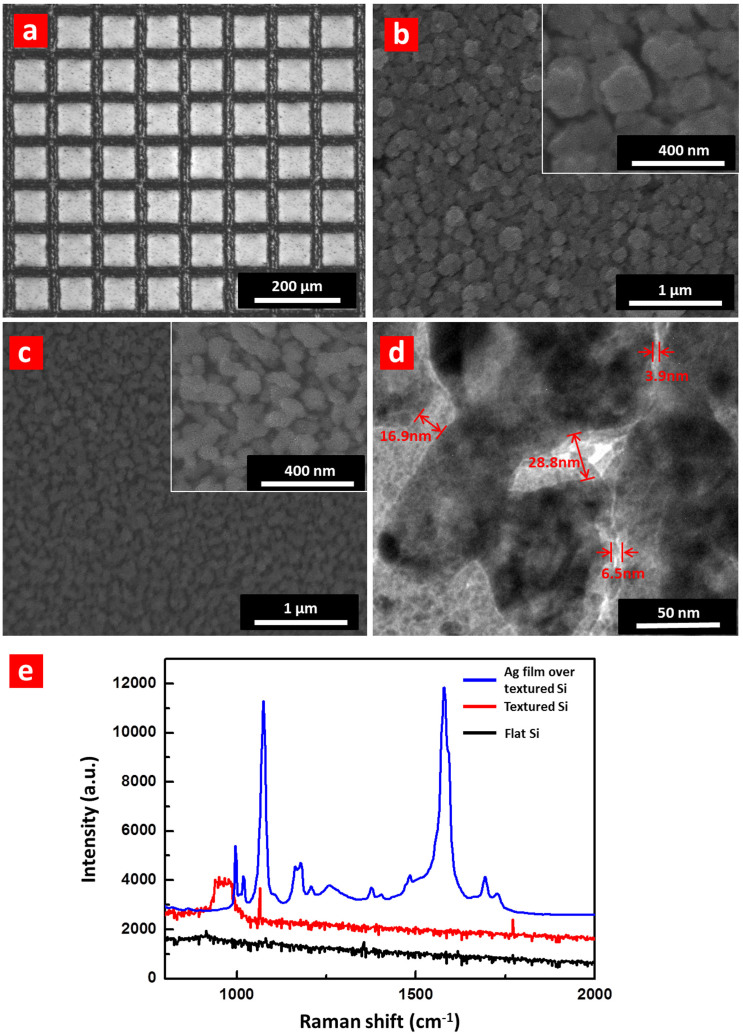
To make large-area SERS substrates, laser processing with 100 μm pitch along both horizontal and vertical directions is applied. The laser ablation configures the Si substrates into microsquare arrays as shown in Figure 3(a). The laser beam irradiates at the boundaries of microsquares. In the center area of the microsquares, there is an aggregation of the Si nanoparticles. The size and shape distributions of Si nanoparticles within the microsquares are crucial for the SERS signal intensity. By changing the laser fluence, the size and shape of nanoparticles can be modified. At a high laser fluence of 21.0 J/cm2, the nanoparticles are in a size distribution from 100 to 300 nm as shown in Figure 3(b). Meanwhile, the shape of the nanoparticles is approximately in sphere. By gradually reducing the laser fluence, the size of nanoparticles in the microsquares becomes smaller. At a lower laser fluence of 14.3 J/cm2, the size of nanoparticles is reduced to less than 100 nm as shown in Figure 3(c). Furthermore, the nanoparticles exhibit various shapes, leading to abundant nanogaps and nanocavities over the Si surface. Figure 3(d) shows the TEM image of small nanogaps created by the nanoparticles’ aggregation. As can be seen, plenty of nanogaps from a few nanometers to tens of nanometers are formed, which function as hotspots during SERS detection. The different laser fluences lead to different nanoparticles’ sizes and shapes. As previously discussed, the size of nanoparticles is determined by the dynamic interaction among the plasma species and air molecules during the laser ablation. Higher input laser fluence tends to induce plasma at higher pressure and temperature16, which gives rise to higher kinetic energy of plasma species. It promotes a stronger interaction between the plasma species and air molecules to form large size nanoparticles. The laser ablation and nanoparticles’ synthesis can provide a rough surface. A further Ag film deposition makes the laser textured Si surfaces as SERS active substrates. Figure 3 (e) shows the SERS spectra of 4-methylbenzenethiol molecules adsorbed on Ag coated laser textured Si in comparison to a flat Si surface and a laser textured Si surface without Ag coating. A significant enhancement in the 1083 cm−1 Raman band can be observed.
Figure 3.
(a) Microscope image of the microsquare array made on Si surface. SEM images within the microsquares of Si surfaces made by the laser ablation at laser fluences of (b) 21.0 and (c) 14.3 J/cm2 (τ = 5 ns, PRR = 100 kHz, laser spot size ~ 20 μm, ν = 100 mm/s). (d) TEM image of the small nanogaps formed by the nanoparticles’ aggregation. (e) The SERS spectra of 4-methylbenzenethiol molecules adsorbed on flat Si surface (500× magnification), textured Si surfaces (500× magnification) and Ag film over the textured Si.
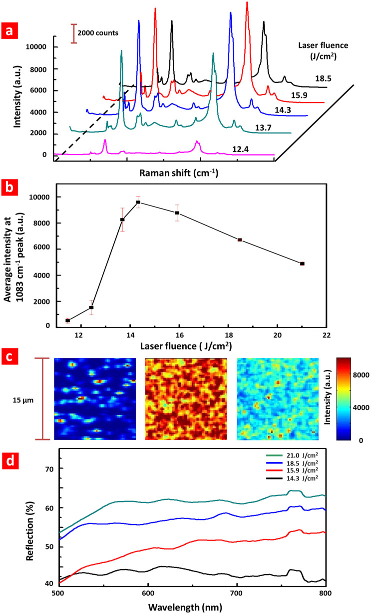
Figure 4(a) shows the SERS spectra of monolayer 4-methylbenzenethiol molecules adsorbed on the Si substrates fabricated at different laser fluences, while Figure 4(b) illustrates the change of average SERS intensity at the 1083 cm−1 Raman band. The SERS performance is poor at a low laser fluence of 11.5 J/cm2. By gradually increasing the laser fluence, better SERS performance is observed due to the aggregation of abundant nanoparticles on the microsquares. When the laser fluence reaches 14.3 J/cm2, the SERS signal is the strongest (~9500 counts at the 1083 cm−1 Raman band). However, the SERS performance becomes worse when further increasing the laser fluence. The observation fits well with the SEM images of the substrates at different laser fluences. In the optimized case, the size of the nanoparticles created by the laser ablation is smaller and the shapes exhibit more diversity. The high density hotspots are generated at the nanogaps, naocavities and nanocorners of the surface structures, which improve the SERS performance. At a higher laser fluence, the size of the nanoparticles increases and the shape of the nanoparticles is much closer to sphere. The fewer nanogaps among the surface structures lead to the lower density of hotspots, which reduces the overall SERS signal intensities. Figure 4(c) shows the Raman map images at 1083 cm−1 Raman band of 15 × 15 μm2 center areas of the microsquares made by the laser at different laser fluences. As can be seen, at a low laser fluence of 11.5 J/cm2, the average SERS signal intensity and the signal uniformity are poor. In this case, there is insufficient energy for the formation and deposition of high density Si nanoparticles, especially in the center areas of the microsquares. The nanoparticles are not uniformly distributed due to the low density of the nanoparticles’ decoration. At a laser fluence of 14.3 J/cm2, both the SERS signal intensity and uniformity are greatly improved. At a further higher laser fluence of 21.0 J/cm2, the signal intensity becomes weaker. It is also in good agreement with the observation in Figures 4(a) and (b). The reflection spectra from 500 nm to 750 nm of the textured substrates fabricated at different laser fluences are shown Figure 4(d). As the laser fluence increases, the reflection gradually increases in this visible range. At a low laser fluence, Ag film over small size nanoparticles (<50 nm) leads to stronger light absorption and localization in the visible range. In this case, the reflection is relatively low but the local field enhancement is more significant, which promotes the SERS detection. At a high laser fluence, scattering becomes dominate when the light irradiates on the Ag film over the large size nanoparticles (>50 nm). The large scattering cross-sections of the nanoparticles lead to the increase of reflection.
Figure 4.
(a) SERS spectra (50 × 50 μm2) of 4-methylbenzenethiol molecules adsorbed on laser ablated Si surfaces and (b) average SERS intensity at the 1083 cm−1 Raman band at different laser fluences. (τ = 5 ns, PRR = 100 kHz, laser spot size ~ 20 μm, ν = 100 mm/s) (c) Raman map image of 15 × 15 μm2 areas on the SERS substrates made by the laser ablation at laser fluences of 11.5, 14.3 and 21.0 J/cm2 from left to right, respectively. (d) Reflection spectra of the SERS substrates in visible spectrum range.
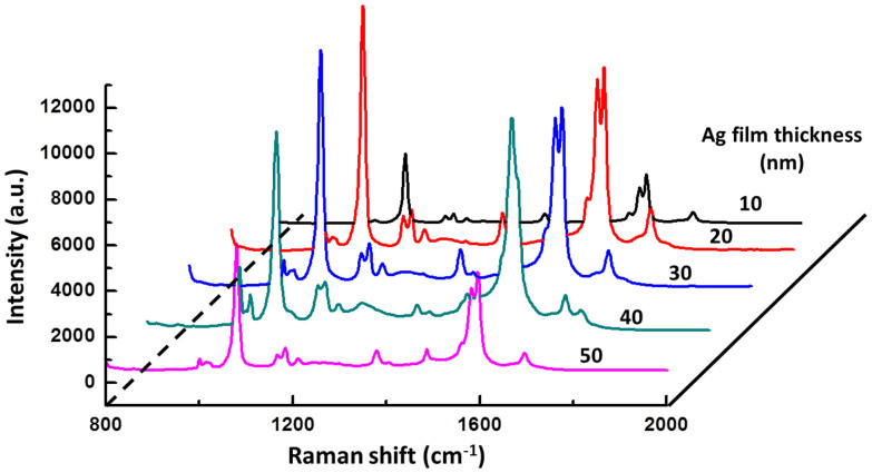
The influence of thickness of the Ag film on the SERS signal intensity is also investigated. The SERS performance of the laser textured Si substrates with different thicknesses of the Ag film is shown in Figure 5. When the thickness of the Ag film is 10 nm, which is below the skin depth of Ag for visible light, the SERS signal intensity is low. With 20 nm Ag film coating, the SERS performance is optimized. When further increasing the thickness of the Ag film, the SERS signal intensities gradually decrease. It is because the thicker Ag film can smear out the surface roughness since the average size of the Si nanoparticles is below 100 nm.
Figure 5. SERS spectra of 4-methylbenzenethiol molecules adsorbed on laser ablated Si surfaces (laser fluence: 14.3 J/cm2) with Ag film coating at different thicknesses.
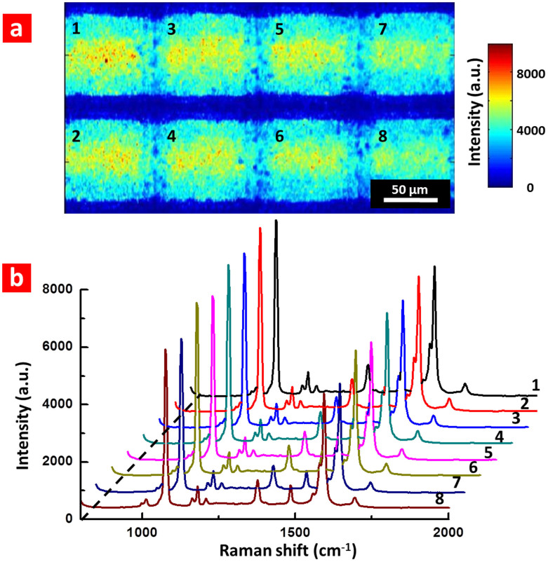
To evaluate the signal uniformity, the SERS spectra are measured from the 8 microsquares on a laser textured substrate with Ag coating as shown in Figure 6(a). The corresponding Raman map image at the 1083 cm−1 Raman band is shown in Figure 6(b). The SERS substrate exhibited uniform 4-methylbenzenethiol spectra with relative standard deviation below 6% for 1083 cm−1, indicating the uniform SERS performance of the substrate. The uniform SERS signals attribute to the similar size and shape distributions of the Si nanoparticles created by the laser ablation inside the microsquares. The laser ablation parameters to configure the microsquares are highly controllable, which also suggests the high reproducibility of the SERS substrates fabricated by our laser micro/nano-processing approach.
Figure 6.
(a) Raman map image at the 1083 cm−1 Raman band of 8 microsquares on the SERS substrates and (b) the corresponding SERS spectra of 4-methylbenzenethiol molecules adsorbed on the microsquares.
The EF is estimated using the equation  1,9, where ISERS is the intensity of the specified Raman band (1083 cm−1) from the probing molecules adsorbed on the SERS substrate, Iref the intensity from the normal Raman measurements, NSERS and Nref the numbers of molecules contributing to ISERS and Iref, respectively. In this work, the average ISERS is around 1619.046 counts per second based on the mean intensity from 3 sample microsquares and the average Iref is around 0.055 counts per second. The laser spot is approximately an ellipse shape with a long axis around 520 nm and a short axis around 380 nm. Taking 4.5 × 10¹⁴ molecules/cm2 for a monolayer of 4-methylbenzenethiol on Ag, approximately 6.825 × 10⁵ molecules are located in the detection volume22. To determine Nref, the detection volume is obtained by measuring the intensity profile of fluorescence beads in ethanol. The measured long axis, short axis and the focus depth of the laser spot are 910 nm, 680 nm and 4.32 μm, respectively. Thus, the effective excitation volume is around 2.1 × 10⁹ nm3. In an ethanol solution of 4-methylbenzenethiol (100 mM/L), Nref is approximately 1.26 × 10⁸ molecules. The average enhancement factor, based on the mean intensity from the three samples at the optimized laser processing parameters, is estimated to be ~5.5 × 10⁶.
Our laser-fabricated-substrates decorated with Ag thin film over nanoparticles exhibit good SERS EF and uniformity. Different from conventional SERS substrates based on metallic thin film over 2D in-plane arranged nanospheres by self-assembled method8, the laser ablated SERS substrate exhibits a pseudo-3D structure with randomly arranged different shaped nanostructures in more than one layer. It contributes to better hotspots’ generation for the SERS signal enhancement.
Our method also provides a rapid two-step fabrication of the SERS substrates. In the SERS substrates prepared by femtosecond laser processing9,10,11, laser irradiation is needed to be carried out almost over the entire sample surface. Meanwhile, the small spot size and short pulse duration are expected to pattern surface structures in nanoscale. However in our design, the laser ablation paths are in the separated lines on the sample surface. The non-irradiated area (microsquares) is exploited for the SERS detection with much larger effective SERS surfaces. The nanostructures are formed by nanoparticles’ deposition during the laser ablation. It leads to a rapid surface fabrication of the SERS substrates.
Conclusions
In summary, we explore a rapid and simple two-step approach to fabricate a large-area SERS substrate. The synthesis of nanoparticles during nanosecond pulsed laser ablation is studied via the SERS detection of molecules adsorbed on Si surface with single line laser ablation. The size of nanoparticles is widely distributed and the small size nanoparticles’ aggregation exhibits better SERS performance. The laser ablation is used to configure the Si surface into microsquare arrays. In each microsquare, there are abundant Si nanoparticles decorated on the flat Si surfaces. Ag thin film deposited over the aggregated nanoparticles can create a high density of hotspots. The laser fluence greatly influences the SERS performance of the substrates. At a laser fluence of 14.3 J/cm2, the size of the nanoparticles decorated in the microsquares is less than 100 nm. In this case, both the field enhancement and the density of hotspots are maximized for the SERS measurement. The SERS substrate shows a high average EF ~ 5.5 × 10⁶ and good uniformity among the microsquares at 6%. This rapid fabrication approach with high controllability can provide huge potential for practical applications of Si based SERS substrates.
Methodology
A nanosecond pulsed laser ablation system is used to fabricate the n-type Si (100) surface. The laser wavelength is 1064 nm, pulse duration (τ) (full width at half maximum, FWHM) 5 ns, pulse repetition rate (PRR) 100 kHz, the laser spot size ~ 20 μm and laser ablation speed (ν) 100 mm/s. The nanosecond pulsed laser ablation can create micropatterns along the ablation path and generate different size nanoparticles, which decorate the Si surface at the same time. The laser beam scans over the Si substrate along both horizontal and vertical directions, dividing the Si surface into many microsquares. In the unexposed area, nanoparticles are aggregated on Si substrates. The ablated Si surfaces are then deposited with Ag (Silver pellets, 99.99% pure, MOS GROUP) thin film by an electron beam evaporator. The morphology of the substrates was characterized by a JEOL JSM-5600 field emission scanning electron microscope.
The laser processed surfaces are functionalized with 2-naphthylamine or 4-methylbenzenethiol molecules. The Ag coated substrates are submerged inside 10 mM 2-naphthylamine or 4-methylbenzenethiol solution made with ethanol for 8 hours to allow the formation of self-assembled monolayer23,24,25. Then the substrates are rinsed in an ethanol solution for 30 seconds and dried by nitrogen. Laser Raman microscope system (Nanophoton RAMANtouch) is used to obtain the SERS spectra of the substrates. The line illumination setup detects 400 spectra simultaneously. A non-polarized 532 nm laser is used. Signals are obtained through a 100× (NA = 0.9) or 20× (NA = 0.45) microscope objective lens and detected by a thermoelectrically cooled CCD array with a 600 g/mm diffraction grating.
Author Contributions
J.Y. and M.H.H. designed the experiments. J.Y., Z.R.D. and J.B.L. performed the experiments and analyzed the data. J.H.T. and Q.H.G. co-wrote the paper. All authors discussed the results and commented on the manuscript.
Acknowledgments
The authors would like to acknowledge the financial support from National Research Foundation, Prime Minister’s Office, Singapore under its Competitive Research Program (CRP Award No. NRF-CRP10-2012-04) and the Economic Development Board (SPORE, COY-15-EWI-RCFSA/N197-1). The authors also thank Prof. Ling Xingyi and Dr. Cui Yan from Chemistry and Biological Chemistry Department at Nanyang Technological University, Singapore on the SERS characterization.
References
- Fan M., Andradec G. F. S. & Brolod A. G. A review on the fabrication of substrates for surface enhanced Raman spectroscopy and their applications in analytical chemistry. Anal. Chim. Acta. 693, 7–25 (2011). [DOI] [PubMed] [Google Scholar]
- Zhang X., Zhou Q., Huang Y., Li Z. & Zhang Z. The nanofabrication and application of substrates for surface-enhanced Raman scattering. Int. J. Spectrosc. 2012, 1–7 (2012). [Google Scholar]
- Cialla D. et al. Surface-enhanced Raman spectroscopy (SERS): progress and trends. Anal. Bioanal. Chem. 403, 27–54 (2012). [DOI] [PubMed] [Google Scholar]
- Sharma B., Frontiera R. R., Henry A., Ringe E. & Duyne P. V. SERS: Materials, applications, and the future. Mater. Today 15, 16–25 (2012). [Google Scholar]
- Peng H. & Miller B. L. Recent advancements in optical DNA biosensors: Exploiting the plasmonic effects of metal nanoparticles. Analyst 136, 436–447 (2011). [DOI] [PubMed] [Google Scholar]
- Stropp J., Trachta G., Brehm G. & Schneider S. A new version of AgFON substrates for high-throughput analytical SERS applications. J. Raman Spectrosc. 34, 26–32 (2003). [Google Scholar]
- Li J. F. et al. Shell-isolated nanoparticle-enhanced Raman spectroscopy. Nature 464, 392–395 (2010). [DOI] [PubMed] [Google Scholar]
- Lin W. et al. Size dependence of nanoparticle-SERS enhancement from silver film over nanosphere (AgFON) substrate. Plasmonics 6, 201–206 (2011). [Google Scholar]
- Diebold E. D., Mack N. H., Doorn S. K., Stephen K. & Mazur E. Femtosecond laser-nanostructured substrates for surface-enhanced Raman scattering. Langmuir 25, 1790–1794 (2009). [DOI] [PubMed] [Google Scholar]
- Fang J., Liu S. & Li Z. Polyhedral silver mesocages for single particle surface-enhanced Raman scattering-based biosensor. Biomaterials 32, 4877–4884 (2011). [DOI] [PubMed] [Google Scholar]
- Negri P. & Dluhy R. A. Ag nanorod based surface-enhanced Raman spectroscopy applied to bioanalytical sensing. J. Biophotonics 6, 20–35 (2013). [DOI] [PMC free article] [PubMed] [Google Scholar]
- Juluri R. R. et al. Coherently embedded Ag nanostructures in Si: 3D imaging and their application to SERS. Sci. Rep. 4, 4633 (2014). [DOI] [PMC free article] [PubMed] [Google Scholar]
- Schmidt M. S., Hübner J. & Boisen A. Large area fabrication of leaning silicon nanopillars for surface enhanced Raman spectroscopy. Adv. Mater. 24, OP11–OP18 (2012). [DOI] [PubMed] [Google Scholar]
- Huang J. A. et al. Ordered Ag/Si nanowires array: wide-range surface-enhanced Raman spectroscopy for reproducible biomolecule detection. Nano Lett. 13, 5039–5045 (2013). [DOI] [PubMed] [Google Scholar]
- Zhou Z. et al. Surface-enhanced Raman scattering substrate fabricated by femtosecond laser direct writing. Jpn. J. Appl. Phys. 47, 189–192 (2008). [Google Scholar]
- Lin C. et al. One-step fabrication of nanostructures by femtosecond laser for surface-enhanced Raman scattering. Opt. Express 17, 21581–21589 (2009). [DOI] [PubMed] [Google Scholar]
- Seto T., Orii T., Hirasawa M. & Aya N. Fabrication of silicon nanostructured films by deposition of size-selected nanoparticles generated by pulsed laser ablation. Thin Solid Films 437, 230–234 (2003). [Google Scholar]
- Fu G. S. et al. The size distribution of Si nanoparticles prepared by pulsed-laser ablation in pure He, Ar or Ne gas. Europhys. Lett. 69, 758–762 (2005). [Google Scholar]
- Zhigilei L. V. et al. Dynamics of the plume formation and parameters of the ejected clusters in short-pulse laser ablation. Appl. Phys. A 76, 339–350 (2003). [Google Scholar]
- Peyre P. & Fabbro R. Laser shock processing: a review of the physics and applications. Opt. Quantum Electron 27, 1213–1229 (1995). [Google Scholar]
- Chen G. X. et al. Carbon nanoparticles based nonlinear optical liquid. Carbon 42, 2735–2777 (2004). [Google Scholar]
- Seo K. & Borguet E. Potential-induced structural change in a self-assembled monolayer of 4-methylbenzenethiol on Au(111). J. Phys. Chem. C 111, 6335–6342 (2007). [Google Scholar]
- Camargo P. H. C., Au L., Rycenga M., Li W. & Xia Y. Measuring the SERS enhancement factors of dimers with different structures constructed from silver nanocubes. Chem. Phys. Lett. 484, 304–308 (2010). [DOI] [PMC free article] [PubMed] [Google Scholar]
- Barea E. M. et al. Design of injection and recombination in quantum dot sensitized solar cells. J. Am. Chem. Soc. 132, 6834–6839 (2010). [DOI] [PubMed] [Google Scholar]
- Cui Y., Hegde R. S., Phang I. Y., Lee H. K. & Ling X. Y. Encoding molecular information in plasmonic nanostructures for anti-counterfeiting applications. Nanoscale 6, 282–288 (2014). [DOI] [PubMed] [Google Scholar]


