Abstract
Using first-principles calculations, we study the electronic properties of few-layer phosphorene focusing on layer-dependent behavior of band gap, work function band alignment and carrier effective mass. It is found that few-layer phosphorene shows a robust direct band gap character, and its band gap decreases with the number of layers following a power law. The work function decreases rapidly from monolayer (5.16 eV) to trilayer (4.56 eV), and then slowly upon further increasing the layer number. Compared to monolayer phosphorene, there is a drastic decrease of hole effective mass along the ridge (zigzag) direction for bilayer phosphorene, indicating a strong interlayer coupling and screening effect. Our study suggests that 1). Few-layer phosphorene with a layer-dependent band gap and a robust direct band gap character is promising for efficient solar energy harvest. 2). Few-layer phosphorene outperforms monolayer counterpart in terms of a lighter carrier effective mass, a higher carrier density and a weaker scattering due to enhanced screening. 3). The layer-dependent band edges and work functions of few-layer phosphorene allow for modification of Schottky barrier with enhanced carrier injection efficiency. It is expected that few-layer phosphorene will present abundant opportunities for a plethora of new electronic applications.
Recent years have witnessed remarkable progress in the application of two-dimensional (2D) materials in transistors and energy conversion1,2. Due to lack of band gap, which dramatically degrades the ON/OFF ratio, pristine graphene is incapable for high-performance field effect transistors. Consequentially, seeking other 2D materials that possess properties complementary to graphene is a fascinating subject of much active research. For example, studies have shown that 2D MoS2 and some other transition metal dichalcogenide (TMD) family members are promising candidates due to their presence of a finite band gap3 and other intriguing electronic properties distinctive from graphene4,5.
More recently, phosphorene, a 2D form of black phosphorus (BP), has attracted increasing attention due to its high carrier mobility, which is up to 1000 cm2V−1s−1 at room temperature, and a moderate band gap, which is about 1.5 eV6,7. As the most stable phosphorus allotrope at ambient condition, bulk black phosphorus can be synthesized under 10 kbar pressure and high temperature, and phosphorene can be obtained by scotch tape-based mechanical exfoliation method6. In contrast to graphene and MoS2, phosphorene is an intrinsic p-type semiconductor8. In addition, a substantial anisotropy in transport behavior was observed recently in few-layer phosphorene with thickness ranging from 2.1 to over 20 nm9. Interestingly, recent studies showed that their anisotropic carrier mobility can be tuned by applying strain10 and their electronic band gap can be engineered by the stacking order11.
While a number of studies have been performed to understand the mechanical12 and electronic properties of monolayer and few-layer phosphorene13, some of their important properties, such as band alignment, work function and carrier effective mass, and their layer-dependent behavior, are still poorly understood. It is well-known that the energy difference between the valence (conduction) band edge of a semiconductor and the work function of a metal electrode determines the Schottky barrier at the metal-semiconductor interface. Hence, an in-depth understanding on the band alignment of the semiconductor is critical for high-performance electronic devices to achieve a high on-current and a low off-current14. However, the band alignment of few-layer phosphorene is still unclear. Moreover, constructing heterostructures consisting of individual monolayers in a precisely controlled stacking sequence with a precisely tuned band offset15,16, is a highly promising route to fabricate 2D materials-based electronic devices. Since monolayer and few-layer phosphorene possess finite and yet moderate band gaps, they are of great potential for being used to construct these heterostructures with other 2D materials. Hence the knowledge on band alignment and work function of monolayer and few-layer phosphorene is indispensable. Unfortunately, both the band alignment and the work function and their thickness-dependent behavior are still unknown, which is clearly an obstacle to hinder their applications in nanoscale electronics and solar energy harvest17.
In this work, we investigate the electronic properties of monolayer and few-layer phosphorene, focusing on their band alignment and work function. We find that a tunable work function up to 0.7 eV can be achieved with increasing the thickness from monolayer (1 L) to five layers (5 L). In addition, there is a significant shift of valence band edge upon thickness variation, which can be useful for tuning Schottky barrier to promote hole injection efficiency. Our work suggests that by harnessing and engineering their thickness-dependent electronic properties, few-layer phosphorene can be promising for applications in high-performance devices.
Results
Thickness dependent band structure
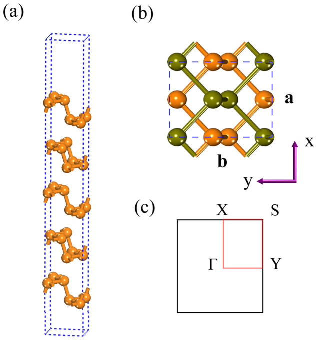
As shown in Fig. 1, the coordination number of each phosphorus atom is three, and the phosphorus atoms are covalently bonded to form a puckered 2D honeycomb structure. The puckered layer is composed of top and bottom ridges along the zigzag direction (a), and each two ridges are connected with surface-normal P-P bonds forming graphene-like armchair lattice (b). The relaxed lattice constant for the 1 L phosphorene is a = 3.34 Å and b = 4.57 Å, in good agreement with previous study9. Similar to graphite, the multilayer BP is held together by van der Waals forces. Hereafter, for the bulk and few-layer BP, the structures are relaxed by using van der Waals corrected optB88 functional, which was shown to be the best estimation for the interlayer gap and binding energy in layered materials like graphene and BN among all the corrected functionals18. In the stacking direction, the ridges on the same side are directly atop each other, but there is a shift of a/2 between adjacent layers along the x direction. The cohesive energy Ecoh for the bilayer phosphorene is defined as (E2L − 2E1L)/8, where E1L and E2L are the total energy of the 1 L and 2 L phosphorene systems respectively, and 8 is the number of phosphorus atoms in the unit cell of 2 L BP. The calculated cohesive energy Ecoh is −55 meV/atom, which is comparable to those of h-BN and graphite (both are around −65 meV/atom)18.
Figure 1.
(a) Side view of the atomic structure of 5 L phosphorene. (b) Top view of bilayer phosphorene, where the atoms in different color representing atoms in different layers. (c) The 2D Brillouin zone for few-layer phosphorene.
To investigate the effect of different exchange-correlation functionals, we compare the band gap of single layer phosphorene using PBE, optB88, and HSE06 methods. The calculated values are 0.84 eV (PBE), 0.84 eV (optB88) and 1.52 eV (HSE06). The band gap calculated using HSE06 is consistent with the experimental observation of 1.45 eV9 and GW result of 1.6 eV13. Owing to the inaccurate description of the electron-electron exchange interaction of the PBE and optB88 approaches, they predict a much smaller band gap (by about 0.7 eV). To better describe the exchange interaction, the band structures for bulk BP and few-layer BP are calculated by using HSE06 hybrid functional starting with the relaxed structure by optB88.
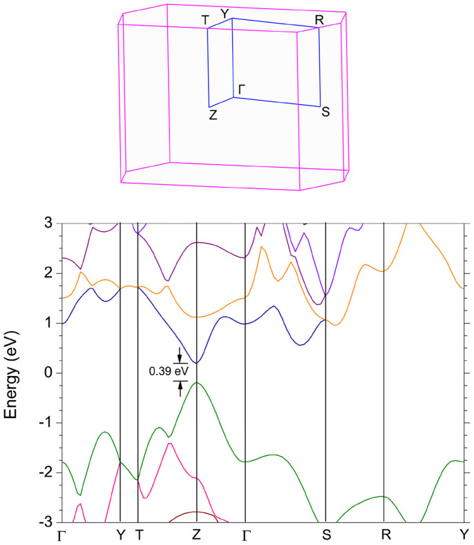
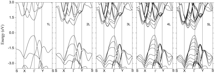
Figure 2 shows the band structure of bulk BP. A direct gap of 0.39 eV at Z point is revealed, which is in good agreement with previous experimental19 and theoretical20,21,22,23 works, thus validating the HSE06 functional in the description of band structure of BP. Figure 3 shows the band structures for 1 L to 5 L. Owing to the quantum confinement effect, the direct band gap at Γ point increases with reducing the thickness. For the bilayer case, the band gap is 1.02 eV, a large drop of 0.5 eV from the 1 L case (1.52 eV). The topology of the band structure for other few-layer phosphorene is similar to that of the 1 L case. For all the layers, there is a clearly asymmetric shape of the band dispersion around the Γ point along Γ-X and Γ-Y branches, suggesting a large anisotropic behavior of electronic structures of few-layer phosphorene, which is in strong contrast to the isotropic electronic structures of graphene, BN and MoS2 layers.
Figure 2. Band structure of the bulk BP calculated by the HSE06 method.
The 2D Brillouin zone is shown in the inset.
Figure 3. Band structures for different few-layer phosphorene systems obtained from HSE06 hybrid functional calculations.
Note that the direct band gap character is maintained for all thicknesses up to 5 L, in contrast to MoS2, which is of a direct band gap character only for monolayer3.
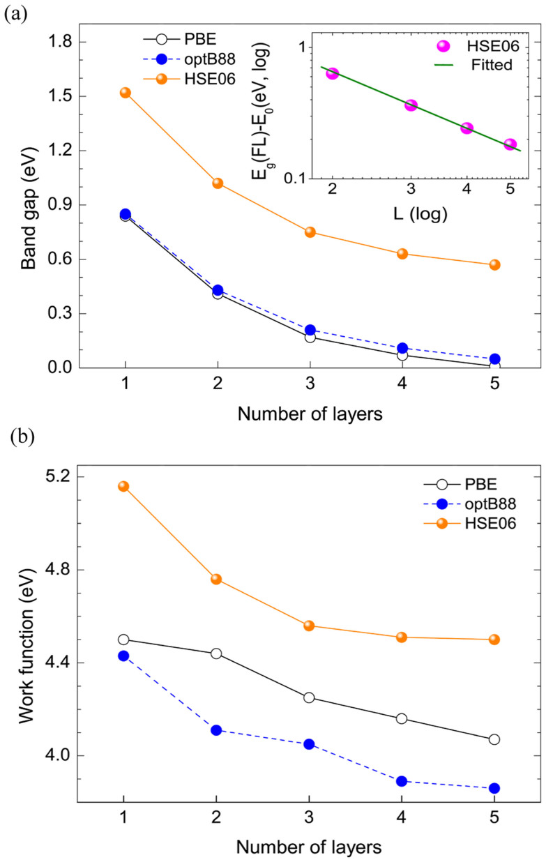
Fig. 4a shows the variations of the band gap with thickness from 1 L to 5 L. It is seen that there is a dramatic decrease in the band gap when the number of layer changes from 1 L to 3 L, whereas the value only decreases slightly when the number of layer is further increased. These results are in good agreement with previous studies9,24. By using the non-local correlation PBE and optB88 functional, we observe that although the values of calculated band gap are much smaller, the thickness dependence is consistent with that predicted by HSE06.
Figure 4.
Variation of the band gap (a) and work function (b) with the thickness of few-layer phosphorene. The inset of (a) shows the band gap versus the number of layers in the log-log scale.
A quantitative expression for layer-dependent band gap
It is well-known that quantum confinement is able to increase the band gap of low-dimensional systems, such as nanowires and nanotubes. For example, it was shown that when the diameter of a nanowire decreases, its band gap increases by following25,26,27, Eg = E0 + C/dα, where Eg is the band gap of the nanowire, E0 is band gap for the bulk material, d is the cylinder diameter of the nanowire, and C and α are fitting parameters. Studies by using first principles calculations and semi-empirical methods showed that the parameter α is between 1 and 1.4 for one-dimensional systems25,26,27. To explore the corresponding quantum confinement effect in few-layer phosphorene, we examine the relationship between the band gap and the number of layers based on HSE06 calculation. The calculation results are shown in the inset of Fig. 4a in the log-log scale. It is seen clearly that there is a notable linear dependence, suggesting that the band gap of few-layer phosphorene also follows the same relation with the number of layers, that is:
 |
where Eg is the band gap of few-layer phosphorene, E0 is the band gap for bulk BP, which is calculated to be 0.39 eV, n is the number of layers. The fitting parameters C and β are 1.62 eV and 1.4, respectively. It is worth noting that this relationship is obtained based on the fitting of the band gap values of few-layer phosphorene from 2 L to 5 L. We find that monolayer phosphorene does not follow the above relationship. The underlying reason may be due to the absence of interlayer coupling. Hence, this band gap expression is only applicable to few-layer phosphorene, in which the interlayer coupling plays the critical role. It is known that the band gap of few-layer phosphorene is usually difficult to measure experimentally. Since the number of phosphorene layers can be obtained by optical measurement15, the above expression provides a convenient formula to predict the band gap value of few-layer phosphorene.
Thickness dependent work function and band alignment
We calculate the work function by subtracting the Fermi energy from the electrostatic potential in the middle of vacuum28,29. Since this procedure can be affected by the chosen exchange-correlation functional, it is expected that the predictions by using these functionals can be different. Fig. 4b shows the variation of the work function with the number of layers. It is seen that the work function for 1 L phosphorene calculated by HSE06, PBE, and optB88 is 5.16, 4.50 and 4.43 eV respectively. Owing to the inaccuracy in considering the self-interaction of electrons by optB88 and PBE functionals, their predicted work functions are expected to be undervalued. Notably, there is a total reduction of the work function of 0.66, 0.43, and 0.57 eV for HSE06, PBE, and optB88, respectively, by increasing the number of layers from 1 L to 5 L. Based on the predictions by HSE06 approach, we see that the work function decreases rapidly from 1 L (5.16 eV) to 3 L (4.56 eV) by 0.6 eV, and then slowly from 3 L (4.56 eV) to 5 L (4.5 eV) by only 0.06 eV, showing the same trend as the band gap change as shown in Fig. 4a. This remarkable change in the work function with the number of layers suggests the possibility to tune the contact resistance by controlling the number of phosphorene layers and selecting suitable contact metals.
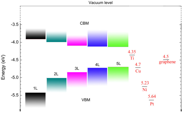
Figure 5 shows the alignment of valence band maximum (VBM) and conduction band minimum (CBM) with respect to the vacuum level for 1 L to 5 L based on the HSE06 calculation. It can be seen that the position of the VBM for 1 L is located at −5.43 eV, and for 3 L at −4.85 eV, and for 5 L at −4.70 eV; and the position of the CBM for 1 L is located at −3.91 eV, and for 3 L at −4.09 eV and for 5 L at −4.13 eV. These results clearly show that there is a rapid upward shift of the VBM and a slow downward shift of CBM. Hence, the adjustment of the VBM with the number of layers is much more intensive than that of the CBM. As an intrinsic p-type semiconductor, the strong layer number-dependent position of VBM in few-layer phosphorene offers a practical route to tune the Schottky barrier height, which can lead to more efficient hole injection and hole transport across the contact.
Figure 5. Variation of valence band maximum (VBM) and conduction band minimum (CBM) for few-layer phosphorene with the number of layers (from 1 L to 5 L) determined from HSE06 calculation.
The VBM and CBM are calculated with respect to the vacuum level. The value of the work function for graphene is taken from Ref. 1 and that for metals from Ref. 29.
Discussion
Doping has been widely used to control the electronic properties of semiconductors. A field effect transistor (FET) can be either n- or p-type, depending on whether electrons or holes are the majority carriers contributed by the dopants. Meanwhile, dopant can distort the lattice of a semiconductor, resulting in enhanced scattering and thus reduced carrier mobility. In recent years, a doping-free technique has been developed in nanoscale electronics, which allows carriers to be supplied directly from the metal electrodes30. For example, when a metal with a high work function is used as electrode, a p-type carbon nanotube FET can be achieved via the Ohmic contact between carbon nanotube valence band and metal30. Conversely, when a metal with a low work function is used as electrode, an n-type carbon nanotube FET can be obtained via the Ohmic contact between the carbon nanotube conduction band and metal. Thus it is the relative position between the conduction/valence band edge of semiconductor and the Fermi level of metal electrode that determines the fundamental characteristics of these FETs. In Fig. 5, for comparison, we also plot the work function of a few metals like Ti, Cu, Ni and Pt, which have been widely used as the electrodes. Remarkably, the tunable conduction/valence band edge of few-layer phosphorene with the number of layers potentially provides a practical means to enhance the performance of its contact with various metal electrodes. However, for real applications, the environmental effects due to impurity and substrate may alter the electronic properties and the work functions of few-layer phosphorene. In addition, as a layered nanomaterial, few-layer BP may suffer from uncertainties arising from the stacking disorder induced by the relative displacement and twisting between the layers. For example, previous study has shown that the stacking variation in bilayer phosphorene can greatly modify the band gap while the direct gap character seems to be unaffected11.
Fig. 3 and Fig. 5 clearly show the layer number-dependent band gap of few-layer phosphorene (from 1.52 to 0.57 eV by HSE06 method). Hence, few-layer phsophorene can be potentially used to construct multi-junction solar cells, which can significantly enhance the energy conversion efficiency by covering the full solar spectrum31. Recent experiment demonstrated that BP transistors indeed respond fast to excitation wavelength ranging from the visible region up to 940 nm32. Importantly, monolayer and few-layer phosphorene all exhibit a direct band gap character, which are in contrast to monolayer and few-layer TMD materials, which usually exhibit a thickness-induced direct-to-indirect transition3. This robust electronic character of monolayer and few-layer phosphorene is ideally suitable for those applications which demand both a high carrier concentration and a good light adsorption efficiency simultaneously.
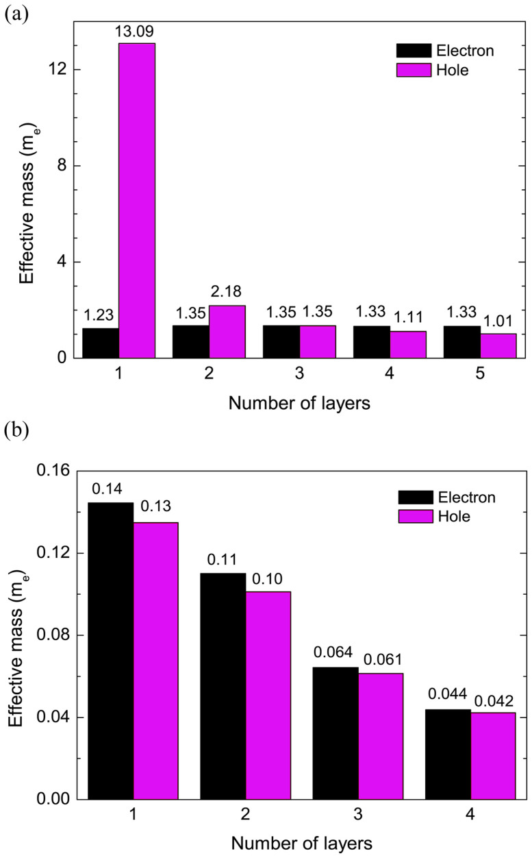
Finally, we examine the thickness-dependent behavior of the effective mass by using the formula  . It should be noted that the calculated effective masses from the HSE06 method is not plotted since it predicts an oscillating effective mass trend with the number of layers due to the substitution of part of the semi-local exchange-correlation functional with the Hartree-Fock exchange. Hence, here, the mass tensor is derived from the calculations by the PBE method. The obtained electron/hole masses along a and b directions are shown in Fig. 6. It is seen that there is a strong anisotropy between hole and electron masses along a and b directions. The electron mass along a (Γ-X) direction is significantly larger (by one order) than that along b (Γ-Y) direction for all the calculated layers. The electron mass of 1 L is 1.23 me along the Γ-X direction and 0.14 me along the Γ-Y direction, in agreement with previous study10. A similar behavior is also observed for holes. For 1 L, the anisotropy of hole mass is extraordinarily large: a two-order difference between the two directions. This strong orientation-dependent effective masses of electron/hole of 1 L phosphorene provides a plausible explanation for the large anisotropic conducting behavior reported recently9. Such strong in-plane anisotropic behavior, which is not found in other 2D materials like BN or MoS2, suggests possible novel applications for phosphorene.
Figure 6. Thickness-dependent effective masses for holes and electrons along zigzag (a) and armchair (b) direction in few-layer phosphorene.
It is interesting to note from Fig. 6a that there is a dramatic decrease of hole mass in 1 L phosphorene (13.09 me) to 2 L phosphorene (2.18 me) along a direction, suggesting a significant change of the band curvature due to the strong interlayer coupling. Since a decrease in the carrier mass generally implies a higher mobility, few-layer phosphorene is likely to perform better than monolayer phosphorene.
In summary, we have investigated the electronic properties of few-layer phosphorene by first-principles calculations. It is found that the band gap, band alignment, work function and carrier effective masses are all dependent on the number of layers. A simple expression is proposed to predict the variation of band gap with the number of phosphorene layers. Importantly, the varied band gap and robust direct band gap character in few-layer phosphorene provides a basis to fabricate multi-junction solar cells which can more effectively harvest solar energy. The layer number-dependent band alignment and work function offer a practical route to tune the Schottky barrier height, which can lead to more efficient hole injection and hole transport across the contact. There is a clear decreasing trend for carrier effective masses with increasing the number of layers, suggesting a higher mobility for multilayer phosphorene than monolayer phosphorene. This is especially true for the hole mass which exhibits a significant thickness dependence along the ridge direction due to the interlayer coupling and screening. In addition, few-layer phosphorene can have an enhanced carrier density and an improved structural stability due to the enhanced interlayer coupling and screening, it is expected that few-layer phosphorene will present abundant opportunities for a plethora of new electronic applications.
Methods
The atomic structure and the stacking order of few-layer phosphorene are shown in Fig. 1. In the present work, the number of few-layer phosphorene is denoted by nL, where n is the number of the monolayer phosphorene, and we consider 1 L to 5 L (0.66 nm to 2.8 nm). All our calculations are performed using the plane wave code Vienna ab initio simulation package (VASP)33 within the framework of density functional theory (DFT). Spin-restricted generalized-gradient approximation with the Perdew-Burke-Ernzerhof functional (PBE)34 and hybrid functionals (HSE06)35 are utilized, together with the projector augmented wave method. The thickness of the vacuum region is greater than 15 Å. The first Brillouin zone is sampled with a 12 × 10 × 1 Monkhorst-Pack grid and a kinetic energy cutoff of 500 eV is adopted. The PBE approach is well-known to have an inaccurate description of the dispersion force and thus a poor estimation of the interlayer distance. Here all the structures are relaxed by using the optimized Becke88 van der Waals (optB88-vdW) functional36. The lattice constant is relaxed until the stress exerted on the cell is less than 0.1 kbar and the forces exerted on the atoms are less than 0.01 eV/Å.
Author Contributions
Y.C. performed the first-principles calculations. G.Z. and Y.-W.Z. contributed to the discussion and writing of the manuscript. All authors reviewed the manuscript.
Acknowledgments
The authors gratefully acknowledge the financial support from the Agency for Science, Technology and Research (A*STAR), Singapore and the use of computing resources at the A*STAR Computational Resource Centre, Singapore.
References
- Lee E. J. H., Balasubramanian K., Weitz R. T., Burghard M. & Kern K. Contact and edge effects in graphene devices. Nat. Nanotech. 3, 486–490 (2008). [DOI] [PubMed] [Google Scholar]
- Ke Q., Tang C., Liu Y., Liu H. & Wang J. Intercalating graphene with clusters of Fe3O4 nanocrystals for electrochemical supercapacitors. Mater. Res. Express 1, 025015 (2014). [Google Scholar]
- Ellis Jason K., Lucero Melissa J. & Scuseria Gustavo E. The indirect to direct band gap transition in multilayered MoS2 as predicted by screened hybrid density functional theory. Appl. Phys. Lett. 99, 261908 (2011). [Google Scholar]
- Cai Y., Zhang G. & Zhang Y.-W. Polarity-Reversed Robust Carrier Mobility in Monolayer MoS2 Nanoribbons. J. Am. Chem. Soc. 136, 6269–6275 (2014). [DOI] [PubMed] [Google Scholar]
- Cai Y., Lan J., Zhang G. & Zhang Y.-W. Lattice vibrational modes and phonon thermal conductivity of monolayer MoS2. Phys. Rev. B 89, 035438 (2014). [Google Scholar]
- Li L. et al. Black phosphorus field-effect transistors. Nat. Nanotech. 9, 372 (2014). [DOI] [PubMed] [Google Scholar]
- Churchill Hugh O. H. & Jarillo-Herrero Pablo Two-dimensional crystals: Phosphorus joins the family. Nat. Nanotech. 9, 330–331 (2014). [DOI] [PubMed] [Google Scholar]
- Takahashi T., Tokailin H., Suzuki S., Sagawa T. & Shirotani I. Highly-angle-resolved ultraviolet photoemission study of a black-phosphorus single crystal. Phys. Rev. B 29, 1105–1108 (1984). [Google Scholar]
- Liu H. et al. Phosphorene: An Unexplored 2D Semiconductor with a High Hole Mobility. ACS Nano 8, 4033–4041 (2014). [DOI] [PubMed] [Google Scholar]
- Fei R. & Yang L. Strain-Engineering the Anisotropic Electrical Conductance of Few-Layer Black Phosphorus. Nano Lett. 14, 2884–2889 (2014). [DOI] [PubMed] [Google Scholar]
- Dai J. & Zeng X. C. Bilayer Phosphorene: Effect of Stacking Order on Bandgap and Its Potential Applications in Thin-Film Solar Cells. J. Phys. Chem. Lett. 5, 1289–1293 (2014). [DOI] [PubMed] [Google Scholar]
- Appalakondaiah S., Vaitheeswaran G., Lebègue S., Christensen N. E. & Svane A. Effect of van der Waals interactions on the structural and elastic properties of black phosphorus. Phys. Rev. B 86, 035105 (2012). [Google Scholar]
- Rudenko A. N. & Katsnelson M. I. Quasiparticle band structure and tight-binding model for single- and bilayer black phosphorus. Phys. Rev. B 89, 201408(R) (2014). [Google Scholar]
- Schottky W. Discrepencies in Ohm's laws in semiconductors. Phys. Z. 41, 570 (1940). [Google Scholar]
- Geim A. K. & Grigorieva I. V. Van der Waals heterostructures. Nature 499, 419–425 (2013). [DOI] [PubMed] [Google Scholar]
- Kang J., Tongay S., Zhou J., Li J. & Wu J. Band offsets and heterostructures of two-dimensional semiconductors. Appl. Phys. Lett. 102, 012111 (2013). [Google Scholar]
- Li Y., Xu C.-Y. & Zhen L. Surface potential and interlayer screening effects of few-layer MoS2 nanoflakes. Appl. Phys. Lett. 102, 143110 (2013). [Google Scholar]
- Graziano G., Klimeš J., Fernandez-Alonso F. & Michaelides A. Improved description of soft layered materials with van der Waals density functional theory. J. Phys. Condens. Matter 24, 424216 (2012). [DOI] [PubMed] [Google Scholar]
- Das S., Zhang W., Demarteau M., Hoffmann A., Dubey M. & Roelofs A. Tunable transport gap in phosphorene. 10.1021/nl5025535 (2014). [DOI] [PubMed]
- Xia F., Wang H. & Jia Y. Rediscovering black phosphorus as an anisotropic layered material for optoelectronics and electronics. Nat. Comm. 5, 4458 (2014). [DOI] [PubMed] [Google Scholar]
- Rudenko A. N. & Katsnelson M. I. Quasiparticle band structure and tight-binding model for single- and bilayer black phosphorus. Phys. Rev. B 90, 085402 (2014). [Google Scholar]
- Peng X., Wei Q. & Copple A. Strain-engineered direct-indirect band gap transition and its mechanism in two-dimensional phosphorene. Phys. Rev. B 90, 085402 (2014). [Google Scholar]
- Qiao J., Kong X., Hu Z.-X., Yang F. & Ji W. High-mobility transport anisotropy and linear dichroism in few-layer black phosphorus. Nat. Comm. 5, 4475 (2014). [DOI] [PMC free article] [PubMed] [Google Scholar]
- Du Y., Ouyang C., Shi S. & Lei M. Ab initio studies on atomic and electronic structures of black phosphorus. J. Appl. Phys. 107, 093718 (2010). [Google Scholar]
- Leu P. W., Shan B. & Cho K. J. Surface chemical control of the electronic structure of silicon nanowires: Density functional calculations. Phys. Rev. B 73, 195320 (2006). [Google Scholar]
- Yan J. A., Yang L. & Chou M. Y. Size and orientation dependence in the electronic properties of silicon nanowires. Phys. Rev. B 76, 115319 (2007). [Google Scholar]
- Yao D., Zhang G. & Li B. A Universal Expression of Band Gap for Silicon Nanowires of Different Cross-Section Geometries. Nano Lett. 8, 4557 (2008). [DOI] [PubMed] [Google Scholar]
- Cai Y. et al. Strain effects on work functions of pristine and potassium-decorated carbon nanotubes. J. Chem. Phys. 131, 224701 (2009). [DOI] [PubMed] [Google Scholar]
- Robinson J. A. et al. Contacting graphene. Appl. Phys. Lett. 98, 053103 (2011). [Google Scholar]
- Peng L.-M., Zhang Z., Wang S. & Liang X. A doping-free approach to carbon nanotube electronics and optoelectronics. AIP Advances 2, 041403 (2012). [Google Scholar]
- Polman A. & Atwater H. A. Photonic design principles for ultrahigh-efficiency photovoltaics. Nature Materials 11, 174–177 (2012). [DOI] [PubMed] [Google Scholar]
- Buscema M. et al. Fast and Broadband Photoresponse of Few-Layer Black Phosphorus Field-Effect Transistors. Nano Lett. 14, 3347–3352 (2014). [DOI] [PubMed] [Google Scholar]
- Kresse G. & Furthmüller J. Efficient iterative schemes for ab initio total-energy calculations using a plane-wave basis set. Phys. Rev. B 54, 11169 (1996). [DOI] [PubMed] [Google Scholar]
- Perdew J., Burke K. & Ernzerhof M. Generalized Gradient Approximation Made Simple. Phys. Rev. Lett. 77, 3865 (1996). [DOI] [PubMed] [Google Scholar]
- Heyd J., Scuseria G. E. & Ernzerhof M. Hybrid functionals based on a screened Coulomb potential. J. Chem. Phys. 118, 8207 (2003). [Google Scholar]
- Becke A. D. Density-functional exchange-energy approximation with correct asymptotic behavior. Phys. Rev. A 38, 3098 (1988). [DOI] [PubMed] [Google Scholar]


