Abstract
Bias-induced oxygen ion dynamics underpins a broad spectrum of electroresistive and memristive phenomena in oxide materials. Although widely studied by device-level and local voltage-current spectroscopies, the relationship between electroresistive phenomena, local electrochemical behaviors, and microstructures remains elusive. Here, the interplay between history-dependent electronic transport and electrochemical phenomena in a NiO single crystalline thin film with a number of well-defined defect types is explored on the nanometer scale using an atomic force microscopy-based technique. A variety of electrochemically-active regions were observed and spatially resolved relationship between the electronic and electrochemical phenomena was revealed. The regions with pronounced electroresistive activity were further correlated with defects identified by scanning transmission electron microscopy. Using fully coupled mechanical-electrochemical modeling, we illustrate that the spatial distribution of strain plays an important role in electrochemical and electroresistive phenomena. These studies illustrate an approach for simultaneous mapping of the electronic and ionic transport on a single defective structure level such as dislocations or interfaces, and pave the way for creating libraries of defect-specific electrochemical responses.
Electroresistance and memristance in nanoscale systems are now among the actively investigated topics in nanoscience and nanotechnology, this interest stemming from applications in non-volatile memories, reconfigurable logics1,2,3, memristive4,5 and neuromorphic electronics6,7. The hallmark of these behaviors is history-dependent responses, including hysteretic behaviors. To date, thousands of studies have been devoted for revealing the macroscopic mechanisms of electroresistive and memristive phenomena8,9,10,11. These phenomena in oxide materials is originated from the electronic field induced metal or oxygen ion dynamics, so in principle, the memristive functionalities derive from atomic scale phenomena. Actually, a number of microscopic studies have been carried out in both anion12,13,14,15 and cation2,16,17,18 mediated electroresistive phenomena as in the macroscopic scale. Multiple groups have explored these systems using conductivity mapping, delineating the spatial localization of the conductive regions19,20,21. In some cases, point I-V spectroscopies were used to extract local I-V curves22,23,24.
Among the local structures, lattice defects such as crystal interfaces and dislocations are expected to play especially significant role in atomic scale phenomena since their structures and compositions are different from bulk phase25,26,27 allowing them to act as high-speed ionic diffusion paths28,29,30,31, nucleation centers for new phases, or electronic conduction pathway. Indeed, dislocations and crystal interfaces are shown to control electroresistive phenomena25,26. Such electroresistive functionalities at local defects are widely studied, however, the detailed mechanisms are still elusive. The problem originates from the complex relationship between electronic conductivity and ionic dynamics. These two types of information cannot be separately obtained in ordinal microscopic technique such as local I-V.
To unravel the intertwined electronic, ionic, and electrochemical phenomena underpinning electroresistive switching, these functionalities must be observed simultaneously, but as separate information, in spatially resolved manner. Recently, electrochemical strain microscopy (ESM)32,33,34 has emerged as a powerful tool for spatially-resolved studies of electrochemical systems. ESM is based on the ionic dynamics induced strain, so the ionic phenomena could be observed separately from the electronic conductive phenomena. In this study, the information of both electronic and electrochemical phenomena are obtained by carrying out ESM voltage spectroscopy and local I-V spectroscopy in the first-order reversal curves (FORC) mode simultaneously35. This approach is applied to the epitaxial NiO, a well-known electroresistive material36,37,38,39. Dislocations and NiO/Pt hetero interfaces of various orientations are introduced into the NiO single crystalline thin film and their effect on the local electroresistive phenomena is revealed for the first time. Especially, NiO/Pt hetero interfaces are well known to enhance electroresistive functionalities40,41. By linking ESM I-V measurement to local structure and composition analysis using scanning transmission electron microscopy (STEM), electron energy loss spectroscopy (EELS) and energy dispersive X-ray spectroscopy (EDS), the relationship between the amount of ionic or vacancy motion, conductive path formation, atomic structure and local composition at the hetero interfaces and dislocations was revealed. Mechanisms for conductive path formation are discussed in terms of strain distributions and the proposed mechanisms are confirmed by finite element strain analysis.
Results
Structural and compositional analysis
In advance to the FORC-ESM analysis, defect structures in the (001) oriented NiO single crystalline thin film are defined using TEM, STEM and related spectroscopic techniques. A 100-nm-thick NiO thin film was deposited on a single crystalline Pt substrate using pulsed laser deposition (PLD). Edge-type dislocations were spontaneously introduced into the NiO film due to the lattice mismatch between the film and substrate of about 9%. The film deposition conditions were controlled so as to create Ni-deficient dislocations. In this state, the dislocations are ferromagnetic in contrast to the antiferromagnetic bulk42, indicative of a local deviation from the stoichiometry.
Typical bright field transmission electron microscopy (TEM) image is shown in Fig. 1a. The black dots indicated by the green arrows in TEM image are pure edge type dislocations. A square type structure is also observed in TEM image as shown by the blue arrow in Fig. 1a. These two types of defects are investigated using advanced TEM methods.
Figure 1. STEM-EELS analysis of a dislocation.

(a) TEM bright field image of NiO single crystalline film at the area including dislocations (green, thin arrows) and a square defect (a blue, thick arrow). (b) Atomic scale HAADF-STEM image of the dislocation core. The perpendicular symbol is showing the core of dislocation. (c) O-K edge EEL spectrum taken at bulk region and the dislocation core. An arrow is showing the pre-peak of O-K edge.
The atomic scale high-angle annular dark-field (HAADF) scanning TEM (STEM) image of a dislocation core viewed from [001] is shown in Fig. 1b. White dots in the image represent the atomic columns consisting of both Ni and O atoms. The Burgers vector of dislocations is determined to be b = a/2 [110], which is pure edge type and is the same vector with dislocations observed in the previous study42. This type of dislocations in NiO film is known to show Ni-deficient structure and exhibit ferromagnetic ordering. To confirm the composition at the dislocation core, electron energy loss spectroscopy (EELS) was carried out. Oxygen K edge EEL spectrum taken at the dislocation core and bulk region are compared in Fig. 1c. Pre-peak of the O-k edge around 528 eV exists only in the spectrum of dislocation core. This peak corresponds to the peak observed in Ni deficient type NiO43. So the dislocations in NiO/Pt are confirmed to be showing a Ni-deficient structure.
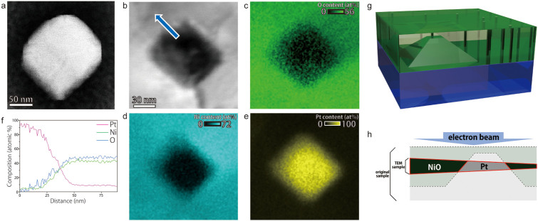
The square structures observed in TEM images are investigated by HAADF-STEM and STEM energy dispersive X-ray spectroscopy (EDS). Low-magnification HAADF-STEM image of the NiO/square structure interface is shown in Fig. 2a. In Fig. 2a, bulk NiO is darker and square structure is brighter. This means that the square structure includes a heavier element; Pt in this case. The contrast at the NiO/Pt interfaces changes gradually, so the interfaces are tilted relative to the electron beam incident direction [001]. Bright field STEM image and EDS chemical composition mappings are shown in Figs. 2b–e. These images clearly show that the square defect consists of pure Pt, with the composition changing gradually at the edges of the Pt square. This can be seen in the line profiles recorded along the arrow in Fig. 2b that are shown in Fig. 2f. The line profiles show that the composition gradually changes from Pt to NiO over a few tens of nm. This means that the NiO/Pt square interfaces are not parallel to the electron beam incident direction [001], so the 3-dimensional shape of the Pt square is that of a truncated pyramid as schematically shown in Fig. 2g. The Pt shape is confirmed by bright field TEM observations (see Supplementary S.1). Given that the surface of the pristine Pt single crystalline is flat with no pyramidal structures prior to the thin film deposition, the Pt pyramids must have formed during the thin film deposition process. In this study, NiO film was deposited by PLD followed by thermal annealing in air. Since thin film was deposited at room temperature and the thermal annealing process is carried out at 1373K, the Pt pyramid seems to have formed during thermal annealing. Apparently, annealing triggered redistribution of phases with minimization of interfacial energy and formation of the preferential NiO(111)/Pt(111) interfacial morphology40. The thickness of NiO film over the Pt pyramid could not be determined because there are some varieties in the size of Pt pyramid, but the thickness is more than a few nanometer as will be discussed in the ESM I-V analysis section. The NiO surface is flat even though the Pt pyramid is formed beneath the NiO film because the thermal annealing temperature is high enough for fast diffusing to flatten the rough surface44.
Figure 2. Chemical composition analysis of a square defect.
(a) HAADF-STEM image of a square defect. (b) Bright field STEM image of a square defect where the EDS mapping was carried out. (c) oxygen, (d) nickel and (e) platinum maps obtained by EDS. (f) Line profiles of chemical compositions extracted at the arrows shown in c. (g) A schematic of Pt pyramid in NiO single crystalline film. Upper green region is the NiO film and lower blue block is the single crystalline Pt substrate. Cylinders schematically show dislocations. (h) A schematic of thin foil for TEM and STEM observations with embedded Pt pyramids.
ESM I-V analysis
Here, spatially resolved ionic behavior in the NiO film with dislocations and Pt pyramids was explored using the ESM voltage spectroscopy45,46. Pt/Cr coated cantilevers were used for the ESM and I-V measurements, thus forming a Pt/NiO/Pt structure. This structure is known for its resistive switching and other electroresistive phenomena. The ESM employs detection of bias-induced reversible strains mediated by ionic motion to probe local electrochemical activity. An electric field is applied to a nanoscale area of the sample surface via an atomic force microscopy (AFM) tip in contact with the surface, leading to ion or vacancy migration. The ionic motion induces local chemical expansion strain, resulting in surface displacement detected by the AFM tip. Here, to maximize the sensitivity through the resonance enhancement and obviate topographic artifacts, the measurements were performed in the band excitation (BE) mode47,48.
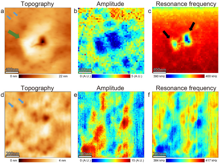
To explore the electrochemical activity on the pristine NiO surface, the ESM imaging was performed. The results are summarized in Fig. 3. In the topographic image of the NiO single crystalline film, two kinds of characteristic defect structures have been observed. The small pits observed both in Figs. 3a and d (see blue arrows), correspond to the dislocations42. The other defect type is associated with a squared hillock, as observed in Fig. 3a (see green arrow). The sample was set to the microscope so that the horizontal axis of the image becomes almost parallel to [010]. Though the sample set direction includes error of about 10 degree due to inaccuracy of sample handling and image drift, the square structures seem to be consist of four <110> edges from Figs. 3a and 5. The size of square defects is in the same order with the Pt pyramids observed in TEM images. Hence this square structure corresponds to the Pt pyramids existing beneath the NiO film. The hillocks are sometimes accompanied by large holes in the center. This is because of strain concentration at the NiO film over the top of Pt pyramids.
Figure 3. BE-ESM images of the NiO film with various types defects.
BE-ESM images of the region with both dislocations and square hills (a–c) and with dislocations only (d–f). a, d AFM topographic image. b, e Amplitude maps at the resonance frequency. c, f Resonance frequency map. Small (blue) arrows indicate dislocations and large (green) arrows indicate a square defect. The region shown by black arrows are showing reverse relationship between resonance frequency map and amplitude map compared to the other region.
Figure 4. Illustration of the FORC ESM and I-V method.
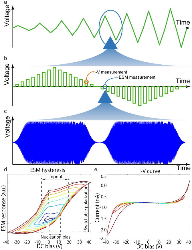
(a) A schematic of a bipolar FORC waveform. (b) A schematic of one triangular wave in the FORC measurements. Triangular waves were formed by a set of pulses, and ESM measurements were carried out in the pulse-off state, whereas I-V measurements were carried out in thepulse-on state. (c) A schematic of two consecutive BE waveforms. A selected number of sinusoidal waves with frequencies within a band centered on the resonance frequency are combined to construct the band excitation waveform. (d) Typical ESM hysteresis loops obtained by averaging the ESM responses for all 50 × 50 measured points in Fig. 5. Various parameters mapped in Fig. 5 are defined here. (e) Typical I-V hysteresis loops obtained by averaging the ESM responses for all 50 × 50 measured points in Fig. 5.
Figure 5. FORC ESM ionic transport maps.
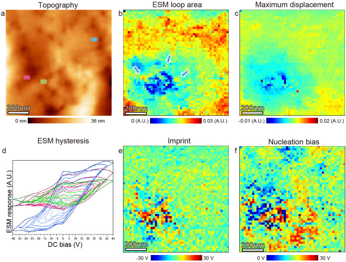
FORC ESM spatial maps of NiO film with dislocations and a square defect. (a) Topographic image of the measured region. Spatial maps of the ESM parameters: (b) ESM loop area (Arrows show the points with large response in the square defect), (c) maximum difference of the surface displacement, (e) imprint, and (f) nucleation bias. (d) ESM hysteresis loops extracted at the points shown by dots in a. Each loop is averaged for six points.
The response amplitude at the resonance frequency against an applied BE waveform with the AC amplitude of 3 V and DC offset of −20 V is mapped for both defects in Fig. 3b and Fig. 3e, respectively. The positive bias is defined to be the direction from the Pt substrate to the NiO film surface. Small ESM amplitude is observed at the dislocations and pyramids. The local variations of resonance frequency in Figs. 3c and f can be ascribed to the topographic effects. The BE waveform is used for reducing crosstalk effect between topography, amplitude, resonance frequency, phase and quality factor, however, the BE method cannot fully remove the crosstalk. In Fig. 3, almost features in amplitude maps correspond to those in resonance frequency maps, though the color contrast is opposite. So almost features in amplitude maps are corresponding with topographic effect, and it is hard to tell whether these features are according to topographic crosstalk or not. Only the region with large hole in Figs. 3a–c is showing positive correlation between resonance frequency and amplitude as indicated by black arrows in Fig. 3c and hence the amplitude response at these regions is not a topographic crosstalk.
The BE-ESM data provide some insight into the local ionic behavior of as-grown state. However, this information is limited and is insufficient to comprehensively characterize electroresistive phenomena associated with formation of conductive path or other ionic motion. Thus, to explore local probing of both ionic and electronic degrees of freedom, we use an approach based on multimodal probing of ionic and electronic behaviors by utilizing FORC method49.
Application of bias to the tip at very low voltages does not alter the chemical state of the system. Hence, the I-V curves are non-hysteric. However, for relatively high voltages, the electric field induces changes in chemical state of the system, and the hysteresis in I-V curves appears as long as the sample has conductivity. Thus, the FORC-based probing can provide insight into the local ionic (from ESM and IV) and electronic (from IV) behavior once both detection modalities are implemented in a single measurement. Here, a triangular voltage sweep consisting of many pulses on a timescale of about 2 ms (Figs. 4a and b) is used. Current was collected in the field-on state and the ESM response was collected in the field-off state by application of the exciting BE waveforms between these pulses (Fig. 4c). Eight triangular waveforms with increasing peak biases from 5 V to 40 V were applied for each point to get information about the history-dependent behavior through the FORC method. Fig. 4d displays hysteresis loops averaged over all of the 50 × 50 measurement points shown in Fig. 5, manifesting a clear loop opening at high biases, which means electroresistive phenomena and ionic motion certainly occurred in the measured region.
Here, the FORC ESM method is applied to an area with both the dislocation pits and a Pt pyramid (Fig. 5a). Shown in Figs. 5b and c are spatial maps of the ESM loop area (the area under the ESM hysteresis loop) and the maximum difference of surface displacement. Both of the spatial maps show low responses at the Pt pyramid. The definitions of parameters (except for loop area) are shown in Fig. 4d. By analyzing individual ESM hysteresis loops in the bulk, the defect interior and the corner of the Pt pyramid as shown in Fig. 5d, the characteristic responses at the square defect is revealed. Specifically, the square defect shows asymmetric hysteretic behavior in contrast to the bulk region with dislocations showing symmetric hysteretic behavior. The ESM loop area and maximum difference of surface displacement are smaller at the Pt pyramid. However, by focusing the area over the Pt pyramid, the corners of the Pt pyramid show relatively larger response, as indicated by the arrows in Fig. 5b. Figs. 5e and f also show similar behavior. Thus the obtained FORC ESM loops provide insight into ionic activity on the NiO surface and defects and its evolution with bias. We further note that in all cases the observed dynamics is reversible. One-time events like tip-induced electroforming can be readily observed as jump-like changes of contrast in ESM associated with formation of large-scale topographic features, and were avoided here.
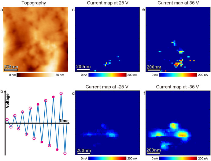
To gain insight into history-dependent electronic behaviors, the FORC I-V spectroscopy49 was realized concurrently with ESM. In this, current was measured in bias-on state during pulsed triangular voltage sweep as shown in Fig. 4b. Current maps at several peak biases are shown in Fig. 6. The triangular voltage sweeps were carried out with gradually increasing peak biases from 5 V to 40 V in 8 sweeps for each point, and the current maps are sampled at the each peak of the triangular waveforms as shown in Fig. 6b. Conductive spots are clearly formed in the maps of negative voltages. In particular, the conductive spots are formed only at four locations, which correspond to the corners of the Pt pyramid. The current maps at positive voltages are also showing conductive spots, and the positions of conductive points in both positive and negative biases are almost overlapping. The corners of the Pt pyramids also show specific contrasts in the ESM loop area map in Fig. 5b, allowing us to conclude that ESM loop area map reflect ionic dynamics during conductive path formation.
Figure 6. Current conductivity maps at selected peak biases.
Current maps recorded simultaneously with FORC ESM shown in Fig. 5. (a) Topographic image of the measured region. (b) A schematic of the applied voltage waveform envelope. Current maps in (c–f) are obtained at the peak biases highlighted by filled circles. Current maps at the peak biases highlighted by open circles are not shown here. Current maps peak biases are: (c) 25 V, (d) −25 V, (e) 35 V, (f) −35 V.
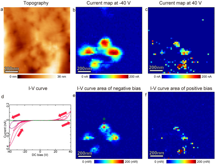
Interestingly, hysteretic electrochemical phenomena are observed in the I-V loops at all conductive spots. I-V loop area and current maps are compared in Fig. 7. Large values in I-V loop area maps (Figs. 7b and c) correspond to large loop opening in I-V loop (Figs. 7e and f), indicative of the degree of conduction hysteresis. Hysteretic phenomena in I-V spectroscopy are mainly associated with the ion or vacancy motion, and here a pronounced ion or vacancy motion is observed at the points of high conductivity. The combination of ESM and I-V spectroscopy techniques, thus, revealed that the ionic mobility is not directly connected to the formation of the conductive spots, suggesting the presence of other factors, and the phenomenon is quite complex because the electronical and electrochemical phenomena appear to be intermixed. The fact that the resistivity is very high at low voltage means there are a few nanometer of NiO film over the top of Pt pyramid. This is because if the thickness of film is less than a few nanometer, the conductivity at around Pt pyramid must be much higher and I-V curve must be more linear according to the direct contact between Pt coated tip and Pt substrate or tunneling effect between them.
Figure 7. I-V loop opening at the conductive points.
Current maps and spatial maps of I-V loop area simultaneously obtained with Fig. 5 and Fig. 6. (a) topographic image of the measured region. (b) Current map at −40 V. (c) Current map at 40 V. (d) Individual I-V loops extracted from the encircled point in e. (e) I-V loop area map calculated for negative branch of I-V loop. (f) I-V loop area map calculated for positive branch of I-V loop.
Finite element modeling
The NiO/Pt interfaces form a bi-axial strain field, which becomes quite complex in the vicinity of Pt pyramids. Here, to explore the effect of strain field on ionic dynamics, we performed finite element calculations. For the calculations, we used the model with one Pt pyramid consist of 4 equivalent {111} and (001). The model also include the region without Pt pyramid, where 100 nm thickness NiO is deposited on flat Pt (001). To represent the static strain field caused by lattice mismatch between the substrate and the film, we used the difference of thermal expansion coefficient for Pt and NiO. We are assuming the phenomena at room temperature, but to introduce the stress consistent with the lattice mismatch, we have “virtually” heated the sample. This virtual heating does not affect the calculation result, except for introducing stress. The heating temperature was determined to be the lattice mismatch is 9%, which is the lattice constant difference between NiO and Pt. Here, we assumed there is no stress relief in the film because of the following reasons. Usually, the strain in the film is relieved by introducing dislocations, grain boundaries and other lattice defects. The NiO film used in this study is single crystal, so including no grain boundaries. Also, no other two dimensional lattice defects are observed in TEM images. So the strain relief should accompanies dislocations, however, by taking the dislocations existing in the NiO film into account, there are still strain consistent with the lattice mismatch of about 8.8%. Hence the dislocation density is not high enough to relief the strain and we need to consider the lattice mismatch in full.
In the calculations, we considered volume change associated with the defect concentration and thermal strain. Under the existence of charged point defects, electric potential and elastic strain energy must be considered in thermodynamic potential in addition to the chemical potential and the activity. By considering the thermodynamic equilibrium across bulk region and the region with strains, the charges originating from the dominant defects can be represented by the defect concentrations (see supplementary information S3). The positive charge concentration cv and the negative charge concentration ce are defined as50:
 |
where  are the oxygen vacancy and extra electron concentrations in bulk,
  and
and  are the partial molar volumes for oxygen vacancy and extra electron, respectively, R is the gas constant, T is temperature, σx, σy and σz are the stress tensor components, F is the Faraday constant and Δϕ0 is the surface potential. The details of parameters are provided in the supplementary information S.1.
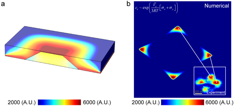
Calculated stress map in the vicinity of the Pt pyramid is shown in Fig. 8a. The strain in NiO around the top facet of the Pt pyramid is much larger than in the bulk region. The extra electron density map at the surface calculated from the stress map and eq. (1) is shown in Fig. 8b. The figure clearly shows that the extra electrons preferentially concentrate at the corners of the top facet of the truncated Pt pyramid. This simulation image matches well with the experimental current map shown as the inset in Fig. 8b.
Figure 8. Strain and carrier density analysis around the Pt pyramid.
(a) 3D strain map around the Pt pyramid calculated by finite element method. (b) Extra electron density map at the surface. The inset and arrows.
Discussions
In contrast to the simple strain distributions around dislocations in the bulk NiO, Pt pyramids form complicated strain field over their tops. The strain around a pure edge-type dislocation can be expressed by a simple plane strain condition. On the other hand, Pt pyramids has four facets and one top plane, and each of these form a Pt/NiO with plane strain due to the lattice mismatch. As a result, a volumetric strain is formed in NiO over the top of the truncated Pt pyramid. Flexibility against an applied stress of a region with volumetric strain is much different from that of a region with plane strain. Regions with plane expansive strain allow for stress relaxation in the mechanically unimpeded direction so long as the Poisson's ratio of NiO is positive52. On the other hand, under volumetric strain, the strain-induced lattice volume change cannot be compensated by mechanical effects, necessitating the vacancy redistribution. Usually lattice shrinks in NiO under positive bias, as positive bias-induced oxygen ions concentration compensates oxygen vacancies, and expands under negative bias35,52,53. These analyses can rationalize why ESM is sensitive to the positive bias and insensitive to the negative bias at the region with volumetric expansive strain and show asymmetric ESM hysteresis in Fig. 5d.
The conductive paths formation can be explained by the amount of strain and the geometry of Pt pyramids. Each face of the pyramids forms expansive strain in the NiO thin film according to the large lattice mismatch between NiO and Pt. The large stresses concentrate at the corners of Pt pyramids. According to the eq. (1), oxygen vacancies and extra electrons concentrate at the region with large strain as far as the eq. S1 in the supplementary information is dominating the defect chemistry in NiO. Furthermore, the voltage concentration occurs at the sharp corners of Pt pyramids. Thus the conductive paths are formed by oxygen vacancies and extra electrons concentration at the corners of Pt pyramids. The proposed mechanisms are confirmed by finite element method calculations. Large stress is applied at the corners of Pt pyramid. Subsequently, oxygen vacancies and extra electrons concentrate at the corners as shown in Fig. 8b.
After the bud for the conductive paths formation is sprout, the conductive paths formation was observed by both ESM in Fig. 5 and I-V in Fig. 7. Hysteresis opened only in the high voltage about −20 or 30 V in I-V, though that opens from low voltage around 10 V in ESM. These results are implying that the ionic motion is started from much lower voltage than the conductive path formation35. The conductive paths are formed by gradual ionic motion started from low voltage, not by abrupt change at a specific voltage.
Conclusions
In summary, the multimodal multidimensional FORC ESM I-V method is applied to the various defects introduced single crystalline NiO. The method enabled us to directly monitor the complex phenomena of electronic and electrochemical behaviors during the formation of the conductive paths. Only the corners of the Pt pyramid underneath the NiO film show conductive path formation absent in the bulk region with Ni-deficient dislocations. The ESM response at the pyramidal defects is asymmetric, with the response being larger at the corner sites. Though the ESM response is asymmetric at the corners of the pyramidal defects, the I-V hysteresis loops were point symmetric. The asymmetry of hysteresis loops is explained by the complex strain field around the Pt pyramid. According to the finite element calculations, the conductive filament formations are induced by the oxygen vacancies and extra electrons concentration around the corners of Pt pyramid due to the large strain. The results are showing complex relationship between electrochemical and electronic behaviors. This high dimensional complexity might be the difficulty present in understanding the underlying mechanisms of electroresistive phenomena, and the method used in this study proved to be a strong tool for overcoming this difficulty.
More generally, combination of the AFM transport imaging methods with the STEM-based characterization of the defect structures will allow building libraries of electronic and ionic behavior for individual defect types. Subsequently, the partial AFM and STEM information will be sufficient to predict overall behavior of the system, model device operation, etc.
Finally, this study illustrates how single defective structures exhibit well-defined electroresistive phenomena. Recently, single defective structures were predicted to be the ultimately limit for nanometer or sub-nanometer scale devices for electronic or magnetic applications25,42. This study show the possibility to expand applications to the electroresistive or electrochemical fields.
Methods
Materials
A 100 nm thick (001)-oriented epitaxial NiO thin film was prepared by pulsed laser deposition on a Pt single crystalline substrate. The substrate temperature was fixed at 300 K, oxygen partial pressure was 1 × 10⁻⁵ Torr, and the laser fluence and frequency were set to 1.5 J cm−2 and 10 Hz, respectively. Following film deposition, the sample was annealed in air at 1,373 K for 0.5 h to improve crystallinity and stoichiometry45. X-ray diffraction studies and TEM observations confirmed the NiO films to be in an epitaxial single-crystal form and of high quality (see supplementary S.2).
AFM measurements
AFM studies were performed with a commercial system (Asylum Research Cypher and Bruker Multimode) controlled externally by a computer via custom-written LabVIEW and MATLAB codes. ESM imaging and FORC ESM were carried out using a BE centered around the resonance frequency of the cantilever in contact with the sample, about 300 ~ 380 kHz in this case. The BE waveform with 3 V amplitude was applied to a Pt/Cr coated probe (BudgetSensors Multi75E-G). Current was measured off of the bottom Pt electrode with the help of a current amplifier (FEMTO, DLPCA-200). Excitation generation and data acquisition was performed by National Instruments cards.
TEM and STEM observations
Conventional TEM observations were performed using a JEM-2010HC (JEOL). High resolution ADF-STEM observations and EELS (Gatan Model 756 Enfina) analysis were conducted with an ARM-200F (JEOL) equipped with an aberration corrector (CEOS). EDS mapping and related bright field-STEM observations are carried out with EM-002BF (JEOL) equipped with twin EDS system (Noran voyger). All TEMs and STEMs were operated at 200 kV. The thin foils for TEM observations were prepared by wedge polishing including no ion milling process.
Finite element calculations
The strain map and the charge concentration map were calculated by finite element methods as described in ref. 47. Further details and parameters are described in the supplementary information S.4.
Author Contributions
I.S., Y.K. and S.V.K. proposed the concept. Y.K., S.J., E.S. and A.K. developed the measurement technique and analysis tools. I.S. and Y.K. performed experiments. I.S. prepared samples. A.T., E.R. and V.S. performed finite element calculations. T.Y., N.S., Y.I. and S.V.K. designed and directed the entire study. I.S., Y.K., N.S. and S.V.K. wrote the manuscript. All authors read and commented on the manuscript.
Supplementary Material
Supplementary information
Acknowledgments
This study was supported in part by the Grant-in-Aid for Scientific Research on Innovative Areas "Nano Informatics" (grant number 25106003) from JSPS. I.S. was supported as JSPS research fellow. N.S. acknowledges support from JST-PRESTO and JSPS KAKENHI Grant number 2368093. The AFM portion of this research was conducted at the Center for Nanophase Materials Sciences (Y.K., S.V.K., E.S., S.J.), which is sponsored at Oak Ridge National Laboratory by the Scientific User Facilities Division, Office of Basic Energy Sciences, U.S. Department of Energy under proposal number CNMS2012-230. STEM/EELS was carried out in the research Hub for Advanced Nano Characterization, the University of Tokyo, under the support of "Nanotechnology Platform" (project No.12024046) by MEXT.
References
- Sawa A. Resistive switching in transition metal oxides. Mater. Today 11, 28–36 (2008). [Google Scholar]
- Waser R., Dittmann R., Staikov G. & Szot K. Redox-Based Resistive Switching Memories - Nanoionic Mechanisms, Prospects, and Challenges. Adv. Mater. 21, 2632–2663 (2009). [DOI] [PubMed] [Google Scholar]
- Waser R. & Aono M. Nanoionics-based resistive switching memories. Nature Mater. 6, 833–840 (2007). [DOI] [PubMed] [Google Scholar]
- Strukov D. B., Snider G. S., Stewart D. R. & Williams R. S. The missing memristor found. Nature 453, 80–83 (2008). [DOI] [PubMed] [Google Scholar]
- Broghetti J. et al. ‘Memristive’ switches enable ‘stateful’ logic operations via material implication. Nature, 464, 8733–876 (2010). [DOI] [PubMed] [Google Scholar]
- Jo S. H. et al. Nanoscale Memristor Device as Synapse in Neuromorphic Systems. Nano Lett. 10, 1297–1301 (2010). [DOI] [PubMed] [Google Scholar]
- Thomas A. Memristor-based neural networks. J. Phys. D: Appl. Phys. 46, 093001 (2013). [Google Scholar]
- Schulman A., Rozenberg M. J. & Acha C. Anomalous time relaxation of the nonvolatile resistive state in bipolar resistive-switching oxide-based memories. Phys. Rev. B 86, 104426 (2012). [Google Scholar]
- Ielmini D. & Cagli C. Size-Dependent Retention Time in NiO-Based Resistive-Switching Memories. IEEE Electron Dev. Lett. 31, 353–355 (2010). [Google Scholar]
- Bi G. & Poo M. Synaptic Modification by Correlated Activity: Hebb's Postulate Revisited. Annu. Rev. Neurosci. 24, 139–166 (2010). [DOI] [PubMed] [Google Scholar]
- Seo K. et al. Analog memory and spike-timing-dependent plasticity characteristics of a nanoscale titanium oxide bilayer resistive switching device. Nanotechnology 22, 254023 (2011). [DOI] [PubMed] [Google Scholar]
- Kwon D. H. et al. Atomic structure of conducting nanofilaments in TiO2 resistive switching memory. Nature Nanotechnol. 5, 148–153 (2010). [DOI] [PubMed] [Google Scholar]
- Yoo I. K. et al. Fractal Dimension of Conducting Paths in Nickel Oxide (NiO) Thin Films During Resistance Switching. IEEE Trans. Nanotechnol. 9, 131–133 (2010). [Google Scholar]
- Fujii T., Arita M., Hamada K., Takahashi Y. & Sakaguchi N. In-situ transmission electron microscopy of conductive filametns in NiO resistance random access memory and its analysis. J. Appl. Phys. 113, 083701 (2013). [Google Scholar]
- Yang Y. et al. Observation of conducting filament growth in nanoscale resistive memories. Nature Commun. 3, 732 (2012). [DOI] [PubMed] [Google Scholar]
- Terabe K., Hasegawa T., Nakayama T. & Aono M. Quantized conductance atomic switch. Nature 433, 47–50 (2005). [DOI] [PubMed] [Google Scholar]
- Hasegawa T., Terabe K., Tsuruoka T. & Aono M. Atomic Switch: Atom/Ion Movement Controlled Devices for Beyond Von-Neumann Computers. Adv. Mater. 24, 252–267 (2012). [DOI] [PubMed] [Google Scholar]
- Nayak A. et al. Controlling the Synaptic Plasticity of a Cu2S Gap-Type Atomic Switch. Adv. Funct. Mater. 22, 3606–3613 (2012). [Google Scholar]
- Kim Y. S. et al. Resistive switching behaviors of NiO films with controlled number of conducting filaments. Appl. Phys. Lett. 98, 192104 (2011). [Google Scholar]
- Son J. Y. & Shin Y. H. Direct observation of conducting filaments on resistive switching of NiO thin films. Appl. Phys. Lett. 92, 222106 (2008). [Google Scholar]
- Yun J. B. et al. Random and localized resistive switching observation in Pt/NiO/Pt. Phys. Stat. Sol. 1, 280–282 (2007). [Google Scholar]
- Lee M. H. et al. Scanning probe based observation of bipolar resistive switching NiO films. Appl. Phys. Lett. 97, 062909 (2010). [Google Scholar]
- Lee M. H. et al. Surface redox induced bipolar switching of transition metal oxide films examined by scanning probe microscopy. Appl. Phys. A 102, 827–834 (2011). [Google Scholar]
- Nardi F. et al. Switching of nanosized filaments in NiO by conductive atomic force microscopy. J. Appl. Phys. 112, 064310 (2012). [Google Scholar]
- Szot K., Speier W., Mihlmayer G. & Waser R. Switching the electrical resistance of individual dislocations in single crystalline SrTiO3. Nature Mater. 5, 312–320 (2006). [DOI] [PubMed] [Google Scholar]
- Lenser Ch. et al. Identification of screw dislocations as fast-forming sites in Fe-doped SrTiO3. Appl. Phys. Lett. 102, 183504 (2013). [Google Scholar]
- Shibata N. et al. Nonstoichiometric dislocation cores in alpha-alumina. Science 316, 82–85 (2007). [DOI] [PubMed] [Google Scholar]
- Arredondo M. et al. Direct Evidence for Cation Non-Stoichiometry and Cotrell Atmospheres Around Dislocation Cores in Functional Oxide Interfaces. Adv. Mater. 22, 2430–2434 (2010). [DOI] [PubMed] [Google Scholar]
- Hojo H. et al. Atomic Structure of a CeO2 Grain Boundary: The Role of Oxygen Vacancies. Nano Lett. 10, 4668–4672 (2010). [DOI] [PubMed] [Google Scholar]
- Love G. R. Dislocation pipe diffusion. Acta Metal. 12, 731–737 (1964). [Google Scholar]
- Luther L. C. Diffusion along dislocation. J. Chem. Phys. 43, 2213–218 (1965). [Google Scholar]
- Balke N. et al. Real Space Mapping of Li-ion Transport in Amorphous Si Anodes with Nanometer Resolution. Nano Lett. 10, 3420–3425 (2010). [DOI] [PubMed] [Google Scholar]
- Kalinin S. et al. Li-ion dynamics and reactivity on the nanoscale. Mater. Today 14, 548–557 (2011). [Google Scholar]
- Jesse S. et al. Electrochemical strain microscopy: Probing ionic and electrochemical phenomena in solids at the nanometer level. MRS Bulletin 37, 651–658 (2012). [Google Scholar]
- Kim Y. et al. Correlative Multimodal Probing of Ionically-Mediated Electromechanical Phenomena in Simple Oxides. Sci. Rep. 3, 2924 (2013). [DOI] [PMC free article] [PubMed] [Google Scholar]
- Kinoshita K., Tamura T., Aoki M., Sugiyama Y. & Tanaka H. Bias polarity dependent data retention of resistive random access memory consisting of binary transition metal oxide. Appl. Phys. Lett. 89, 103509 (2006). [Google Scholar]
- Kim D. C. et al. Electrical observations of filamentary conductions for the resistive memory switching in NiO films. Appl. Phys. Lett. 88, 202102 (2006). [Google Scholar]
- Lee S. R. et al. Resistive memory switching in epitaxially grown NiO. Appl. Phys. Lett. 91, 202115 (2007). [Google Scholar]
- Sullaphen J., Bogle K., Cheng X., Gregg J. M. & Valanoor N. Interface mediated resistive switching in epitaxial NiO nanostructures. Appl. Phys. Lett. 100, 203115 (2012). [Google Scholar]
- Huang Y. C. et al. Improvement of resistive switching in NiO-based nanowires by inserting Pt layers. Appl. Phys. Lett. 101, 153106 (2012). [Google Scholar]
- Lee S. R. et al. Investigation of Interface Formed between Top Electrodes and Epitaxial NiO Films for Bipolar Resistance Switching. Jpn. J. Appl. Phys. 49, 031102 (2010). [Google Scholar]
- Sugiyama I. et al. Ferromagnetic dislocations in antiferromagnetic NiO. Nature Nanotechnol. 8, 266–270 (2013). [DOI] [PubMed] [Google Scholar]
- Koyama Y., Mizoguchi T., Ikeno H. & Tanaka I. Electronic structure of lithium nickel oxide by electron energy loss spectroscopy. J. Phys. Chem. B 109, 10749–10755 (2005). [DOI] [PubMed] [Google Scholar]
- Joshi U. S., Takahashi R., Matsumoto Y. & Koinuma H. Structure of NiO and Li-doped NiO single crystalline thin layers with atomically flat surface. Thin Solid Films 486, 214–217 (2005). [Google Scholar]
- Balke N. et al. Nanoscale mapping of ion diffusion in a lithium-ion battery cathode. Nature Nanotechnol. 5, 749–754 (2010). [DOI] [PubMed] [Google Scholar]
- Kumar A., Ciucci F., Morozovska A. N., Kalinin S. V. & Jesse S. Measuring oxygen reduction/evolution reactions on the nanoscale. Nature Chem. 3, 707–713 (2011). [DOI] [PubMed] [Google Scholar]
- Jesse S., Kalinin S. V., Proksch R., Baddorf A. P. & Rodriguez B. J. The band excitation method in scanning probe microscopy for rapid mapping of energy dissipation on the nanoscale. Nanotechnol. 18, 435503 (2007). [Google Scholar]
- Jesse S. & Kalinin S. V. Band excitation in scanning probe microscopy: sines of change. J. Phys. D: Appl. Phys. 44, 464006 (2011). [Google Scholar]
- Evgheni S. et al. Probing Local Ionic Dynamics in Functional Oxides at the Nanoscale. Nano Lett. 13, 3455–3462 (2013). [DOI] [PubMed] [Google Scholar]
- Sheidon B. W. & Shenoy V. B. Space Charge Induced Surface Stresses: Implications in Ceria and Other Ionic Solids. Phys. Rev. Lett. 106, 216104 (2011). [DOI] [PubMed] [Google Scholar]
- Park G. S. et al. Observation of electric-field induced Ni filament channels in polycrystalline NiOx film. Appl. Phys. Lett. 91, 222103 (2007). [Google Scholar]
- Groppo E. et al. Growth of NiO on Ag(001): Atomic Environment, Strain, and Interface Relaxations Studied by Polarization Dependent Extended X-ray Absorption Fine Structures. J. Phys. Chem. B 107, 4597–4606 (2003). [Google Scholar]
- Lee S. R. et al. Role of oxygen vacancies formed between top electrodes and epitaxial NiO films in bipolar resistance switching. Curr. Appl. Phys. 12, 369–372 (2012). [Google Scholar]
Associated Data
This section collects any data citations, data availability statements, or supplementary materials included in this article.
Supplementary Materials
Supplementary information


