Abstract
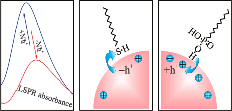
Nanoparticles exhibiting localized surface plasmon resonances (LSPR) are valuable tools traditionally used in a wide field of applications including sensing, imaging, biodiagnostics and medical therapy. Plasmonics in semiconductor nanocrystals is of special interest because of the tunability of the carrier densities in semiconductors, and the possibility to couple the plasmonic resonances to quantum confined excitonic transitions. Here, colloidal Cu2–xSe nanocrystals were synthesized, whose composition was shown by Rutherford backscattering analysis and electron dispersive X-ray spectroscopy, to exhibit Cu deficiency. The latter results in p-type doping causing LSPRs, in the present case around a wavelength of 1100 nm, closely matching the indirect band gap of Cu2–xSe. By partial exchange of the organic ligands to specific electron trapping or donating species the LSPR is fine-tuned to exhibit blue or red shifts, in total up to 200 nm. This tuning not only provides a convenient tool for post synthetic adjustments of LSPRs to specific target wavelength but the sensitive dependence of the resonance wavelength on surface charges makes these nanocrystals also interesting for sensing applications, to detect analytes dressed by functional groups.
Keywords: colloidal nanocrystals, plasmon resonance, ligand exchange, interfacial charge transfer
1. Introduction
Localized surface plasmon resonances (LSPRs) arise from resonant oscillations of free charges in the presence of light. Nanoparticles exhibiting LSPRs are highly attractive due to strong local field enhancements,1−3 causing amplified scattering and absorbance of light.1−3 These properties have been widely utilized in biology and biomedicine, for instance, for molecule specific imaging and for the diagnosis of diseases like cancer,4−8 for photothermal therapy,4−6,9 or for real-time optical sensing with zeptomole sensitivity.10 While traditionally for such purposes nanoparticles made of various noble-metals have been used, whose LSPRs are predominantly found in the visible spectral region,4,11,12 in the last years, efforts have been made toward the synthesis of heavily doped metal-oxides and semiconductors exhibiting plasmonic response.6,13−19 The key advantage of using semiconductors for nanoplasmonics is that their free carrier concentrations, and thus their LSPRs, can be tuned by doping, or in device structures even by applied electric fields.20 As shown by the pioneering work of J. M. Luther et al.,13 in quantum dots of the semiconductor dicopper(I) sulfide (Cu2–xS) high p-type self-doping is achieved due to numerous copper-deficient stoichiometries. In their material, the LSPRs were found close to wavelengths of 2 μm, and the resonance wavelengths could be slightly tuned by postsynthetic oxidation of the nanocrystals. While the reversibility of the postsynthetic tuning of the LSPRs by oxidation/reduction was demonstrated subsequently for Cu2–xSe as well as for Cu2–xTe,16,18 here we expand the methods to tune the LSPRs by a further tool, namely ligand exchange. In contrast to the case of Ag nanoparticles, where the length of the alkyl chains of the ligands was varied to tune the LSPR by changing the dielectric function of the surrounding medium,10 in this work, the electron trapping/donating functional head groups are the key parts of the ligands, which are exchanged in order to control the hole concentration in the nanocrystals. This concept is demonstrated here for the established Cu2–xSe nanocrystals,17 providing a tunability of the LSPR over a range of approximately 200 nm around a center wavelength of 1100 nm. This LSPR closely matches to the indirect band gap of Cu2Se, making coupling of plasmonic near-fields to excitonic transitions straightforward.
2. Experimental Section
2.1. Chemicals
Copper chloride (CuCl, 99.995+%), 1-dodecanethiol (DDT, CH3(CH2)11SH, 98+%) and technical oleylamine (TOA, CH3(CH2)7CH=CH(CH2)8NH2, 70%) were received from Aldrich; elemental selenium (Se, 99.999%) and 1-dodecylphosphonic acid (DDPA, CH3(CH2)11PO(OH)2, 95%) were obtained from Alfa Aesar. Oleylamine (OA, 80–90% of C18 chains) was bought from Acros Organics. Absolute ethanol (ACS grade) and n-hexane, toluene and chloroform were supplied by Merck and VWR Chemicals, respectively. All chemicals were used as received.
2.2. Synthesis
The synthesis of Cu2–xSe nanocrystals was performed by modifying the procedure introduced by the Swihart group.17 Briefly, the reactions were performed in OA with a total amount of 35 mL. The injection solution consisted of 0.5 mmol (49.4 mg) of copper chloride and 10 mL of OA mixed together within a glovebox at room temperature. Then the flask was connected to an argon filled Shlenk line, and the mixture was heated to 130 °C for 1 h. The color of the mixture changed within this time from deep blue to clear yellow. As the selenium precursor, an equimolar quantity of Se powder (39 mg) was mixed with 25 mL of OA, and the solution was heated up to 300 °C for 30 min, to form a clear solution. After the temperature was decreased to 260 °C, the hot metal precursor solution was injected. This lowers the temperature of the reaction mixture to 220 °C, which was found to be optimal for seed nucleation and nanocrystal growth.17 The yellow colored solution turned black immediately after injection and after a growth time of 4 min, the growth was quenched by cooling down the reaction flask in a water bath. The crude solution was transferred to test tubes and 5 mL of toluene, and 7 mL of absolute ethanol was added to the mixtures. After centrifugation at 3000 rpm for 3 min, the blue supernatant was removed and the precipitates were redispersed in 5 mL of toluene, with dropwise addition of up to 20 μL of OA. Seven milliliters of ethanol was added to the solution, and the nanocrystals were again isolated by centrifugation. The washing procedure was repeated at least three times, yielding each time a clearer supernatant. Finally, the nanocrystals were redispersed in 4 mL of toluene and centrifuged at 1000 rpm for 1 min, to remove small amount of bulk and poorly stabilized nanocrystals. The supernatant was filtered through a 0.2 μm Polytetrafluoroethylene (PTFE) (VWR) filter. We checked that the syntheses modifications we made still provide the same LSPR properties as are described in ref (17). We also noticed that replacing OA by TOA essentially does not affect the obtained LSPR properties of copper(I) selenide nanocrystals.
2.3. Ligand Exchange
To partly exchange the nanocrystal ligands, 200 μL of colloidal solution containing about 4 mg of nanocrystals was mixed with 3 mL of 0.1–20 mM DDT or 1–200 mM DDPA in toluene. The colloidal solution was sonicated for several minutes to accelerate OA ligand removal and attachment of thiolic or phosphonic ligands.
2.4. Characterization
UV–vis-near-infrared (UV–vis-NIR) absorbance was measured in a quartz cuvette with an optical path length of 10 mm by using a Cary 5E UV–vis-NIR spectrophotometer. Scanning electron microscopy (SEM) was carried out on a ZEISS 1540XB machine, operating at 3 kV. Transmission electron microscopy (TEM) was performed with a JEOL-2011 FasTEM instrument, operated at a 100 kV acceleration voltage, to visualize the nanocrystals and to obtain electron diffraction patterns of selected areas. In addition, electron dispersive X-ray spectroscopy (EDXS) mapping was performed with a FEI OSIRIS scanning transmission electron microscopy (STEM) instrument operated at 200 kV. Quantitative analysis of EDXS spectra was done by the Cliff–Lorimer method. For quantitative analysis of elemental concentrations Rutherford backscattering spectrometry (RBS) using 2 MeV He+ ions was employed. Samples for TEM and RBS/SEM measurements were prepared by drop casting of diluted nanocrystal solution on carbon coated copper grids and silicon wafers, respectively.
3. Results and Discussions
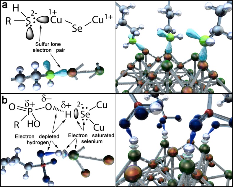
The general idea of this work is to tune the LSPRs in heavily doped copper(I) chalcogenide semiconductor nanocrystals by attachment of carrier trapping or donating ligands. Hole accepting ligands were previously identified by static and dynamic photoluminescence quenching experiments performed with CdSe based nanocrystal quantum dots.21−23 For CdSe, a ligand exchange from trioctylphosphine to thiol molecules resulted in an effective luminescence quenching, which was attributed to the removal of photogenerated holes from the nanocrystals toward the ligands. Analogous to the case of the thiol–CdSe interface24 in the copper(I) chalcogenide, the thiol molecule will be attached to the nanocrystals surfaces via donating the sulfur lone electron pair to the copper cation. This donation results in formation of a coordinate bond between the sulfur atoms of the thiol ligands and the Cu+ atoms of the nanocrystal surface (sketched in Figure 1a). Then the nanocrystals surface hole states from the Cu atoms became passivated, which altered the total nanocrystal surface charge. As a consequence, the average electron density in the nanocrystal is increased, which is equivalent to a decrease of the average nanocrystal hole density. Considering once again the situation of luminescent CdSe nanocrystals, we find also a case where the opposite can be achieved. Ultrasmall CdSe nanocrystals are reported to exhibit pronounced defect emissions from surface trap states, which can be altered by the attachment of phosphonic acid ligands.25 According to the density functional theory study of ligand bindings on CdSe surfaces, acidic ligands can coordinate through the hydroxyl hydrogen to the electron-rich surface sites.26 The phosphonic/phosphoric acids and their derivatives form strong intramolecular hydrogen bonds, leading easily to polarized O–H groups,27,28 which bind to the electron-rich Se atoms on the nanocrystals surface. In both possible cases, the dipole–dipole hydrogen bond as well as in the polarized proton dative bond, the electrons from the surface Se will be attracted toward the hydrogen (Figure 1b) and thus become trapped between nanocrystal and ligand, forming a surface trap state. Thus, the phosphonic acids exhibit an experimentally proven electron withdrawing nature,25 which again changes the surface charge and thus increases the overall nanocrystals hole concentration.
Figure 1.
Schematic presentation of the charge trapping/donating ligands, attached to the Cu2–xSe nanocrystal surfaces. (a) Thiolic and (b) phosphonic ligands. Besides the ball-and-stick model of the nanocrystal and the ligands, the tentative shapes of the relevant electron wave functions also are shown.
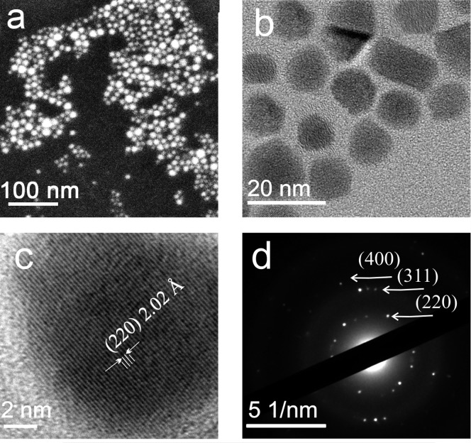
The LSPRs in semiconductor nanocrystals depend strongly on variations of the synthetic conditions, such as molar ratios of precursors, reaction temperatures and choice of reaction and postreaction solvents. Thus, as starting material we have chosen here heavily self-doped p-type Cu2–xSe, for which synthetic recipes, delivering nanocrystals with strong near-infrared LSPRs absorption due to cation deficiencies, are well established.6,14 The as-synthesized nanocrystals have a mean size of 9.2 ± 2 nm, and are slightly irregular in shape (Figure 2). Their crystalline structure is revealed by high resolution TEM. In the high resolution image in Figure 2c lattice fringes are resolved, whose distance of 2 Å closely matches to the (220) lattice planes of Berzelianite (a cubic crystal with the space group Fm3m).17 This assignment is further confirmed by the diffraction reflexes observed in the selected area electron diffraction pattern in Figure 2(d), which can also be unambiguously indexed to specific lattice plane distances of the cubic Cu2Se crystal structure.17
Figure 2.
Properties of the Cu2–xSe nanocrystals. (a,b) Representative SEM and TEM images. (c) Monocrystalline nature of the nanocrystals is revealed by the high resolution TEM image and by (d) the selected area electron diffraction pattern.
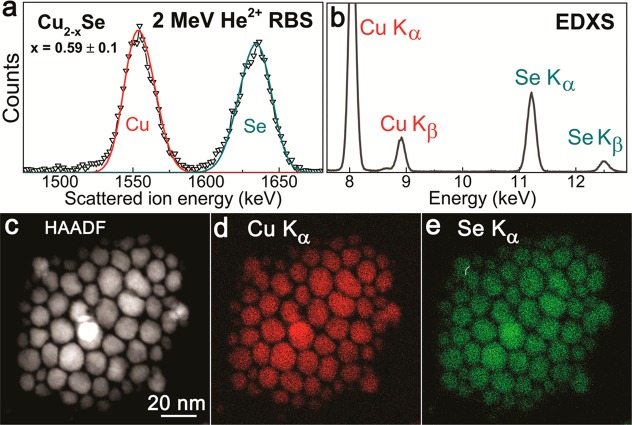
To test the nanocrystals composition, elemental analysis was performed on several submonolayer thick samples prepared on Si substrates by means of RBS. The spectrum in Figure 3a exhibits distinct peaks that can by simple scattering kinematics associated with Cu and Se. A fit to the peak area permits us to determine the relative concentrations of Cu and Se without the need for reference samples, by making use of well-established scattering cross sections. All RBS spectra clearly confirm the desired Cu deficiency and a substoichiometric Cu content Cu2–xSe with an average x = 0.6 ± 0.1 is deduced by fits of the data (see solid lines in Figure 3 calculated by SIMNRA.29 To study the particle-to-particle homogeneity of the nanocrystals, in addition, EDXS mapping was performed by STEM. The images of the Se Kα and Cu Kα maps (Figure 3b–d), show that all nanocrystals, even though they vary substantially in size, are of homogeneous composition. From the EDX spectrum in Figure 3b, the k-factor method (Cliff–Lorimer) for the Cu and Se K-lines provides 62.7 ± 1.9 wt % Cu and 37.3 ± 1.2 wt % Se, which coincides almost perfectly with Cu2–xSe, with x = 0. This Cu content is in disagreement with the value obtained by RBS; however, the EDXS spectra reveal next to the L- and K-lines of Cu and Se also lines of S, Cl and Ni. These additional lines originate either from residuals of the precursors, or from artifacts, provided by scattering at the TEM grid or microscope parts. Measurements on empty Cu grid supported TEM substrates and on SiN TEM grids revealed always the presence of Ni and Cu signals, which, when subtracted from the data given in Figure 3c, provide substantial reduced Cu contents, corresponding to x = 0.1–0.3. Thus, the EDXS confirms the desired Cu deficiency in the nanocrystals.
Figure 3.
Elemental analyses of the Cu2–xSe nanocrystals. (a) Experimental RBS spectra (open triangles) and simulations (solid lines). (b–e) EDXS spectrum and elemental maps of the nanocrystals.
Most important for plasmonic nanocrystals are their optical properties. Thus, optical absorbance measurements have been performed on the nanocrystals kept in toluene (Figure 4). For the as-synthesized sample, a pronounced LSPR peak is observed with its maximum at a wavelength of 1100 nm, which closely matches the results shown in ref (17), for nanocrystals synthesized in the same way. Thus, the same tentative band diagram, as it was suggested in ref (19), can be used for interpretation of the absorption features in Figure 3. According to ref (30), Cu1.85Se exhibits two interband optical transitions, a direct transition at 2.1 eV (590 nm) and an indirect transition at 1.3 eV (950 nm). Thus, the absorption minimum at 600 nm, followed by smaller wavelength by an absorption onset, is caused by the direct band gap and the fundamental absorption of Cu2–xSe. The much weaker absorbance due to the indirect band gap is hidden under the much more pronounced absorbance of the plasmonic peak, caused by the collective oscillations of the free holes in the valence band under light excitation. To partially exchange the nanocrystal ligand shell, DDT was added in low concentrations to the toluene solution. The addition of 0.1 mM DDT resulted already in a significant alteration of the LSPR peak (Figure 4), which is found to become reduced in intensity and red-shifted in wavelength. We should note that shortening the ligands alkyl length, from OA to DDT the (CH)n chain is reduced from 18 to 12, would result in a blue shift of the LSPR, caused by a change of the dielectric function of the medium surrounding the nanocrystals. This fact has been used previously to detect the formation of a monolayer of small-molecules adsorbed on Ag nanoparticles with zeptomole sensitivity.10 The observed red shift is thus not due to the change of the ligands alkyl group, but rather due to the ligands functional group. As discussed above, the thiol is providing electrons to the nanocrystals surface, which is effectively reducing the overall averaged hole concentration in the nanocrystal, resulting in the observed red shift. This shift could be further enhanced by increasing the DDT concentration and for 1 mM DDT the red shift amounts to 200 nm. This tuning range, obtained by postsynthetic ligand treatments, is as large as that previously obtained during synthesis by change of the synthetic conditions.17,18 Furthermore, by changing the type of ligands from electron donating to electron withdrawing ones, the tuning range could be even increased. Treating the nanocrystal solution with DDPA, which has the same alkyl length as DDT, indeed provides blue shifts up to 50 nm. To obtain these blue shifts, however, much larger concentrations of DDPA are required than as for DDT. Concentrations substantially above 50 mM are not feasible to tune the LSPR further, because, at these concentrations, the nanocrystals suffer from etching.
Figure 4.
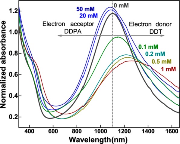
Cu2–xSe nanocrystals, tuning the plasmon resonance by ligand attachment. Absorbance spectra obtained in solution without and with various concentrations of DDPA and DDT ligands.
The observed LSPRs are directly correlated to the nanocrystals hole concentrations and the latter can be extracted from the experimental results by making use of the well-known relations13 for the LSPR angular frequency
| 1 |
and bulk plasmon frequency
| 2 |
Taking into account the dielectric permittivity of toluene as medium (εm) and the effective mass of holes (mh) for Cu2–xSe from ref (31), the hole density (Nh) can be evaluated (γ is the experimentally determined width of the LSPR). These evaluation show that the hole density in the as synthesized Cu2–xSe is approximately 1.26 × 1021 cm–3 and it was altered by +7% and −17% by the attachment of electron tapping and donating ligands, respectively (Table 1). It should be noted that the LSPR frequency for nanocrystals, which are small enough to be described in the static dipole approximation, as is described by eqs 1 and 2, does not depend on the nanocrystal dimensions. Thus, the observed quality factor is probably not suffering substantially from the finite size and shape distribution of the nanocrystal batches synthesized here, but it is rather determined by the nanocrystals surface properties, damping the LSPR resonance by surface scattering of free carriers.13 The latter will depend on the nanocrystals ligand shell, which is shown above to be a powerful tool to tune the nanocrystals carrier concentration and LSPR. In fact, the observed quality factors between 2 and 3 are comparably advantageous to those observed in doped tungsten oxide nanocrystals,32 exhibiting LSPRs at approximately the same wavelengths with quality factors below 2, and are slightly smaller as the values obtained in Au nanorods with appropriate aspect ratios to exhibit LSPRs around 1000 nm.11
Table 1. Parameters Deduced from Fits of the Cu2–xSe Nanocrystals Plasmon Resonances.
| sample | λsp (nm) | ωsp (s–1) | γ (s–1) | ωp (s–1) | Np (cm–3) | h/NC | Δh/NC |
|---|---|---|---|---|---|---|---|
| Cu2–xSe-DDPA | 1075 | 1.74 × 10¹⁵ | 5.58 × 10¹⁴ | 4.41 × 10¹⁵ | 1.35 × 10²¹ | 433 | 29 |
| Cu2–xSe | 1102 | 1.70 × 10¹⁵ | 4.83 × 10¹⁴ | 4.26 × 10¹⁵ | 1.26 × 10²¹ | 404 | |
| Cu2–xSe-DDT | 1271 | 1.48 × 10¹⁵ | 6.34 × 10¹⁴ | 3.88 × 10¹⁵ | 1.04 × 10²¹ | 336 | –68 |
The ligand induced shift of the LSPR frequency allows us also to evaluate the efficiency of the obtained ligand exchange. While for the as synthesized nanocrystal, the number of holes per NC is on the order of 400 (Table 1); the number of ligands bound to the nanocrystal surface, about 4 of them are attached per square nanometer,10 is approximately 1000. Assuming that the increase/decrease of free holes per nanocrystal (Δh/NC) due to the treatment with DDPA/DDT is solely ascribed to the electron withdrawing/donating nature of each ligand, only less than 7% of the surface ligands need to be changed to obtain the observed shift of the LSPR resonance. Assuming that shifts as small as 1 nm could be experimentally easily resolved, even the attachment of one single electron donating/accepting ligand to the nanocrystals surface could be detected by the shift of the plasmon resonance. This points toward a possible applicability of such plasmonic semiconductor nanocrystals, namely for sensing of analytes with functional groups.
4. Conclusions
In contrast to metal nanoparticles, heavily doped semiconductor nanocrystals exhibiting LSPRs offer the possibility to tune the optical response by control of their carrier density. Here, the carrier density is controlled by a partial ligand exchange, performed in solution. By attachment of electron trapping or donating ligands, the LSPR was tuned over approximately 200 nm. This is demonstrated for Cu2–xSe nanocrystals, which are well-known to exhibit LSPRs due to p-type doping provided by a Cu deficiency. These results show (i) the sensitivity of the LSPRs to the nature of the functional groups of the attached ligands, which could be used also for sensing of analytes, (ii) the possibility to tune the LSPRs after the synthesis to the desired wavelengths and (iii) the feasibility to have materials whose plasmonic and excitonic optical transitions closely match each other.
Acknowledgments
O.A.B acknowledges the support from the ÖAD-GmbH in form of a “Stipendium der Stipendienstiftung der Republik Österreich”. This work was supported by the Austrian Science Fund FWF via a SFB project IR-ON (F25) and project J3317-N27. W.H. gratefully acknowledges use of the services and facilities of the “Energie Campus Nürnberg” and financial support through the “Aufbruch Bayern” initiative of the state of Bavaria. H.G. gratefully acknowledges the group of C. Feldmann, KIT for the use of the FEI Tecnai Osiris microscope.
Author Contributions
The paper was written through contributions of all authors. All authors have given approval to the final version of the paper.
The authors declare no competing financial interest.
References
- Willets K. A.; Van Duyne R. P. Localized Surface Plasmon Resonance Spectroscopy and Sensing. Annu. Rev. Phys. Chem. 2007, 58, 267–297. [DOI] [PubMed] [Google Scholar]
- Hao E.; Schatz G. C. Electromagnetic Fields around Silver Nanoparticles and Dimers. J. Chem. Phys. 2004, 120, 357–366. [DOI] [PubMed] [Google Scholar]
- Chen Y.; Ming H. Review of Surface Plasmon Resonance and Localized Surface Plasmon Resonance Sensor. Photonic Sens. 2012, 2, 37–49. [Google Scholar]
- Jain P. K.; Huang X.; El-Sayed I. H.; El-Sayed M. A. Noble Metals on the Nanoscale: Optical and Photothermal Properties and Some Applications in Imaging, Sensing, Biology, and Medicine. Acc. Chem. Res. 2008, 41, 1578–1586. [DOI] [PubMed] [Google Scholar]
- Gong J.; Li G.; Tang Z. Self-Assembly of Noble Metal Nanocrystals: Fabrication, Optical Property, and Application. Nano Today 2012, 7, 564–585. [Google Scholar]
- Liu X.; Swihart M. T. Heavily-Doped Colloidal Semiconductor and Metal Oxide Nanocrystals: An Emerging New Class of Plasmonic Nanomaterials. Chem. Soc. Rev. 2014, 43, 3908–3920. [DOI] [PubMed] [Google Scholar]
- Xiong B.; Zhou R.; Hao J.; Jia Y.; Hea Y.; Yeung E. S.. Highly Sensitive Sulphide Mapping in Live Cells by Kinetic Spectral Analysis of Single Au-Ag Core-Shell Nanoparticles. Nat. Commun., 2013, 4. DOI: 10.1038/ncomms2722. [DOI] [PubMed] [Google Scholar]
- Liu X.; Lee C.; Law W.-C.; Zhu D.; Liu M.; Jeon M.; Kim J.; Prasad P. N.; Kim C.; Swihart M. T. Au–Cu2–xSe Heterodimer Nanoparticles with Broad Localized Surface Plasmon Resonance as Contrast Agents for Deep Tissue Imaging. Nano Lett. 2013, 13, 4333–4339. [DOI] [PubMed] [Google Scholar]
- Hessel C. M.; Pattani V. P.; Rasch M.; Panthani M. G.; Koo B.; Tunnell J. W.; Korgel B. A. Copper Selenide Nanocrystals for Photothermal Therapy. Nano Lett. 2011, 11, 2560–2566. [DOI] [PMC free article] [PubMed] [Google Scholar]
- McFarland A. D.; Van Duyne R. P. Single Silver Nanoparticles as Real-Time Optical Sensors with Zeptomole Sensitivity. Nano Lett. 2003, 3, 1057–1062. [Google Scholar]
- Eustis S.; El-Sayed M. A. Why Gold Nanoparticles are More Precious than Pretty Gold: Noble Metal Surface Plasmon Resonance and its Enhancement of the Radiative and Nonradiative Properties of Nanocrystals of Different Shapes. Chem. Soc. Rev. 2006, 35, 209–217. [DOI] [PubMed] [Google Scholar]
- Mock J. J.; Barbic M.; Smith D. R.; Schultz D. A.; Schultz S. Shape Effects in Plasmon Resonance of Individual Colloidal Silver Nanoparticles. J. Chem. Phys. 2002, 116, 6755–6759. [Google Scholar]
- Luther J. M.; Jain P. K.; Ewers T.; Alivisatos A. P. Localized Surface Plasmon Resonances Arising from Free Carriers in Doped Quantum Dots. Nat. Mater. 2011, 10, 361–366. [DOI] [PubMed] [Google Scholar]
- Comin A.; Manna L. New Materials for Tunable Plasmonic Colloidal Nanocrystals. Chem. Soc. Rev. 2014, 43, 3957–3975. [DOI] [PubMed] [Google Scholar]
- Liu X.; Wang X.; Swihart M. T. Cu2–xS1–ySey Alloy Nanocrystals with Broadly Tunable Near-Infrared Localized Surface Plasmon Resonance. Chem. Mater. 2013, 25, 4402–4408. [Google Scholar]
- Saldanha P. L.; Brescia R.; Prato M.; Li H.; Povia M.; Manna L.; Lesnyak V. Generalized One-Pot Synthesis of Copper Sulfide, Selenide-Sulfide, and Telluride-Sulfide Nanoparticles. Chem. Mater. 2014, 26, 1442–1449. [Google Scholar]
- Liu X.; Wang X.; Zhou B.; Law W.-C.; Cartwright A. N.; Swihart M. T. Size-Controlled Synthesis of Cu2-xE (E = S, Se) Nanocrystals with Strong Tunable Near-Infrared Localized Surface Plasmon Resonance and High Conductivity in Thin Films. Adv. Funct. Mater. 2013, 23, 1256–1264. [Google Scholar]
- Kriegel I.; Jiang C.; Rodríguez-Fernández J.; Schaller R. D.; Talapin D. V.; da Como E.; Feldmann J. Tuning the Excitonic and Plasmonic Properties of Copper Chalcogenide Nanocrystals. J. Am. Chem. Soc. 2012, 134, 1583–1590. [DOI] [PubMed] [Google Scholar]
- Scotognella F.; Della Valle G.; Kandada A. R. S.; Zavelani-Rossi M.; Longhi S.; Lanzani G.; Tassone F.. Plasmonics in Heavily-Doped Semiconductor Nanocrystals. Eur. Phys. J. B, 2013, 86. DOI: 10.1140/epjb/e2013-40039-x. [DOI] [Google Scholar]
- Llordés A.; Garcia G.; Gazquez J.; Milliron D. J. Tunable Near-Infrared and Visible-Light Transmittance in Nanocrystal-in-Glass Composites. Nature 2012, 500, 323–326. [DOI] [PubMed] [Google Scholar]
- Jiang Z.-J.; Leppert V.; Kelley D. F. Static and Dynamic Emission Quenching in Core/Shell Nanorod Quantum Dots with Hole Acceptors. J. Phys. Chem. C 2009, 113, 19161–19171. [Google Scholar]
- Liu I.-S.; Lo H.-H.; Chien C.-T.; Lin Y.-Y.; Chen C.-W.; Chen Y.-F.; Su W.-F.; Liou S.-C. Enhancing Photoluminescence Quenching and Photoelectric Properties of CdSe Quantum Dots with Hole Accepting Ligands. J. Mater. Chem. 2008, 18, 675–682. [Google Scholar]
- Mohamed N. B. H.; Haouari M.; Zaaboub Z.; Nafoutti M.; Hassen F.; Maaref H.; Ouada H. B.. Time Resolved and Temperature Dependence of the Radiative Properties of Thiol-Capped CdS Nanoparticles Films. J. Nanopart. Res., 2014, 16. DOI: 10.1007/s11051-013-2242-9. [DOI] [PMC free article] [PubMed] [Google Scholar]
- Liang Y.; Thorne J. E.; Parkinson B. A. Controlling the Electronic Coupling between CdSe Quantum Dots and Thiol Capping Ligands via pH and Ligand Selection. Langmuir 2012, 28, 11072–11077. [DOI] [PubMed] [Google Scholar]
- Schreuder M. A.; McBride J. R.; Dukes A. D. III; Sammons J. A.; Rosenthal S. J. Control of Surface State Emission via Phosphonic Acid Modulation in Ultrasmall CdSe Nanocrystals: The Role of Ligand Electronegativity. J. Phys. Chem. C 2009, 113, 8169–8176. [Google Scholar]
- Rempel J. Y.; Trout B. L.; Bawendi M. G.; Jensen K. F. Density Functional Theory Study of Ligand Binding on CdSe (0001), (000-1), and (11-20) Single Crystal Relaxed and Reconstructed Surfaces: Implications for Nanocrystalline Growth. J. Phys. Chem. B 2006, 110, 18007–18016. [DOI] [PubMed] [Google Scholar]
- Leuchs M.; Zundel G. Polarizable Acid-Acid and Acid-Water Hydrogen Bonds with H3PO2, H3PO3, H3PO4, and H3AsO4. Can. J. Chem. 1979, 57, 487–493. [Google Scholar]
- Vilčiauskas L.; Tuckerman M. E.; Bester G.; Paddison S. J.; Kreuer K.-D. The Mechanism of Proton Conduction in Phosphoric Acid. Nat. Chem. 2012, 4, 461–466. [DOI] [PubMed] [Google Scholar]
- Mayer M. SIMNRA, A Simulation Program for the Analysis of NRA, RBS and ERDA. AIP Conf. Proc. 1999, 475, 541–544. [Google Scholar]
- Al-Mamun; Islam A. B. M. O.; Bhuiyan A. H. Structural, Electrical and Optical Properties of Copper Selenide Thin Films Deposited by Chemical Bath Deposition Technique. J. Mater. Sci.: Mater. Electron. 2005, 16, 263–268. [Google Scholar]
- Gorbachev V. V.; Putilin I. M. Some Parameters of Band Structure in Copper Selenide and Telluride. Phys. Status Solidi A 1973, 16, 553–559. [Google Scholar]
- Manthiram K.; Alivisatos A. P. Tunable Localized Surface Plasmon Resonances in Tungsten Oxide Nanocrystals. J. Am. Chem. Soc. 2012, 134, 3995–3998. [DOI] [PubMed] [Google Scholar]


