Abstract
Perovskite solar cells (PeSCs) have been considered one of the competitive next generation power sources. To date, light-to-electric conversion efficiencies have rapidly increased to over 10%, and further improvements are expected. However, the poor device reproducibility of PeSCs ascribed to their inhomogeneously covered film morphology has hindered their practical application. Here, we demonstrate high-performance PeSCs with superior reproducibility by introducing small amounts of N-cyclohexyl-2-pyrrolidone (CHP) as a morphology controller into N,N-dimethylformamide (DMF). As a result, highly homogeneous film morphology, similar to that achieved by vacuum-deposition methods, as well as a high PCE of 10% and an extremely small performance deviation within 0.14% were achieved. This study represents a method for realizing efficient and reproducible planar heterojunction (PHJ) PeSCs through morphology control, taking a major step forward in the low-cost and rapid production of PeSCs by solving one of the biggest problems of PHJ perovskite photovoltaic technology through a facile method.
Organic solar cells (OSCs)1,2,3, dye-sensitized solar cells (DSSCs)4,5, and organic/inorganic hybrid perovskite solar cells (PeSCs)6,7, have been intensively investigated as competitive to inorganic silicon solar cells due to their potential for cost-efficient, light-weight, and flexible device fabrication8,9,10. To date, power conversion efficiencies (PCEs) of over 10% have been achieved by synthesizing donor/acceptor semiconducting materials and optimizing the processing conditions in OSCs11 and by developing novel dyes and redox mediators in DSSCs12. However, despite this substantial progress, there are challenges for high efficiency, mainly ascribed to the strong exciton binding energy in OSCs and to the inefficient electron transport process13, as well as the poor stability due to the liquid electrolyte components in DSSCs14,15.
Meanwhile, hybrid solar cells employing organic/inorganic perovskite materials (e.g., CH3NH3PbI(3−x)Clx and CH3NH3PbI3) with direct bandgaps, high absorption coefficients, long exciton diffusion lengths, and excellent charge transport properties as light-harvesters and carrier conductors have been recently recognized as one of the promising next generation photovoltaics capable of resolving the aforementioned challenges16. By utilizing these superior properties, high-performance perovskite-based cells have been reported by several groups6,17,18. In particular, most state-of-the-art PeSCs with PCEs of >10% were realized by depositing perovskite materials onto a mesostructured TiO2 scaffold acting as the electron transport layer19,20,21.
After these successful demonstrations of mesostructured TiO2-based PeSCs, it was revealed that planar heterojunction (PHJ) architectured PeSCs are also possible due to the long carrier lifetimes and diffusion lengths of perovskite materials22,23. In particular, PHJ PeSCs can be more attractive for real applications, considering that mesostructured PeSCs have a disadvantage of the high temperature process necessary to obtain a high-quality and compact TiO2 layer, which can limit further applications, especially in flexible architectures6,20. To overcome this aspect, PHJ PeSCs were recently demonstrated with the exclusion of the mesoporous TiO2 layer, and comparable performances to those of TiO2-based PeSCs were realized in several groups18,19. Despite these successful demonstrations, there is a critical drawback in the field of PHJ perovskite photovoltaics; the uncontrolled precipitation of perovskite generates large morphological deviations, leading to large efficiency fluctuations in the resulting devices17,24. In particular, variable device performance has been regarded as the most urgent issue to be solved for the realization of reliable PeSCs25.
To solve this problem, diverse methods such as vacuum deposition, vapor-assisted solution processes, and sequential deposition have been employed19,26,27,28. However, the aforementioned methods are hard to facilitate the low-cost and rapid production of PeSCs because they require cost-intensive and time-consuming processing by vacuum deposition and vapor-assisted solution methods, respectively19,26. In particular, two-step sequential deposition methods have been largely successful for fabricating homogeneous perovskite thin-films; however, they also frequently result in peeling of the perovskite film during deposition29. Therefore, it is urgently necessary to develop a simple, fast, and efficient approach for fabricating uniform and complete perovskite films with enhanced controllability and high reproducibility for the commercial application of PeSCs.
In this study, we demonstrate highly efficient and reproducible CH3NH3PbI3-based PHJ PeSCs by using a small amount of N-cyclohexyl-2-pyrrolidone (CHP) additive as a morphology controller. Perovskite precursor in DMF solution, containing 5 vol% CHP, forms homogeneous nucleation sites and makes slow crystallization of perovskite structure due to the high boiling point and extremely low vapor pressure of CHP, respectively, thus finally enabling complete coverage of highly smooth film morphologies similar to that obtained by vacuum deposition method. In particular, the efficiencies of CHP:DMF-based PeSCs were dramatically increased to up to 10% with an extremely small standard deviation value of 0.14%, which is superior to that of PeSCs without CHP (the PCE of 3.63 ± 1.61%), in which an inhomogeneous and incomplete perovskite film leads to poor efficiency and high device-to-device deviation. This novel method for realizing uniform and full-coverage perovskite films by using a small amount of CHP as a morphology controller could be a facile way to improve both the efficiency and the reproducibility of PeSCs.
Results
Influence of the morphology controller on perovskite film formation
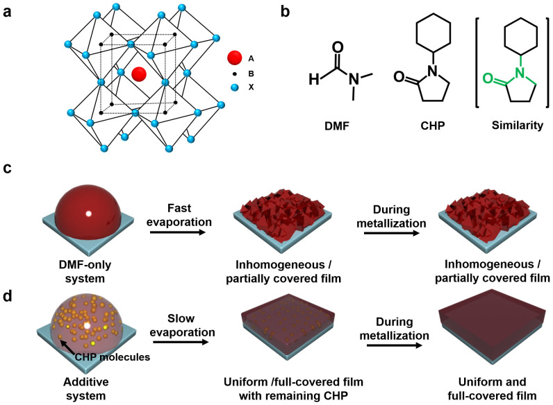
In Figure 1a, the unit cells of perovskite compounds are defined as crystals in the ABX3 structure, composed of corner-sharing BX6 octahedra and the A component on the corners of the lattice30. In the case of organometal trihalide perovskites, the unit cell consists of an A organic cation, a B metal cation, and an X halide anion. In this study, we used CH3NH3PbI3 with a tetragonal perovskite structure as a photoactive layer due to its faster production compared to MAPbI(3−x)Clx, where a long thermal treatment of approximately 1 h is needed to form the perovskite crystal17,31,32. As mentioned above, a high-quality perovskite film is extremely important in the planar architecture to achieve efficient and reproducible PeSCs24,25,32,33. Thus, we used CHP as a morphology controlling additive by simply adding it to the DMF solution. The chemical structures of CHP and DMF are depicted in Figure 1b.
Figure 1. Schematic illustration of the perovskite film formation.
(a) Illustration of the crystal structure of CH3NH3PbI3 perovskite and (b) chemical structures of DMF and CHP. Schematic illustration of perovskite film formation in (c) DMF only and in (d) a CHP additive system.
The concept of additive-aided morphology control is quite simple; however, we hypothesized that there would be several requirements for a morphology controller, as follows: First, the additive must have an extremely low vapor pressure than DMF (2.9 mmHg at room temperature) to minimize the rapid evaporation of solvent during the spinning process and a high boiling point to achieve uniform atmosphere during thermal annealing process which obtain a uniform and full-covered film. Second because the CH3NH3PbI3 crystal is formed by the reaction of equivalent molar ratios of methylammonium iodide and lead(II) iodide, enough solubility in both components is critical for ensuring monolithic CH3NH3PbI3 crystalline films. Third, the additive must exhibit high miscibility with the main solvent, such as DMF. Based on the above requirements, we chose CHP as an additive because it has a high boiling point of 286°C, an extremely low vapor pressure of 0.05 mmHg at room temperature, and high-miscibility with the conventionally used DMF solvent due to their structural similarity, as shown in Figure 1b. In addition, because both CH3NH3I and PbI2 are soluble in CHP at concentrations of up to 0.6 and 0.25 g/ml, respectively, which do not hinder the solubility of DMF. Therefore, CHP could be utilized as an efficient morphology controller by preventing changes in the CH3NH3PbI3 composition after deposition.
Following the above strategies, the steps of perovskite film formation in DMF-only and the DMF with CHP additive system are illustrated in Figure 1c and d. In general, due to the fast evaporation of DMF-only systems, the perovskite crystal forms too rapidly to control its morphology during the spinning process. As a result, an inhomogeneous and leaky film, which causes direct contact between the hole and electron extraction layers, is produced24. In the additive system, we hypothesized that the high boiling point and an extremely low vapor pressure of CHP would prevent the rapid crystal formation of CH3NH3PbI3 and produce homogeneous nucleation via the remaining CHP molecules in the film, thus finally producing a uniform and dense perovskite crystalline film through the evaporation of CHP during the metal deposition step, as shown in Figure 1d.
Thin-film morphology characterization
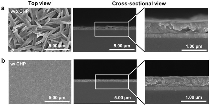
To evaluate the possibility of using additive-aided morphology control, we investigated the surface morphologies of the perovskite film by scanning electron microscopy (SEM), as shown in Figure 2. For the films processed from the DMF-only system, inhomogeneous and incomplete coverage of the perovskite films in the top-view SEM images and small and large pores inside the perovskite film in the cross-sectional SEM images can be easily observed due to the fast evaporation of the DMF solvent during the spinning process, which is indicative of the difficulty of obtaining perovskite films with good coverage and uniform thickness using a DMF-only system, as shown in Figure 2a.
Figure 2. Thin-film topology characterization.
Top-view and cross-sectional SEM images of the CH3NH3PbI3 films (a) without and (b) with the use of the CHP additive as a morphology controller.
On the other hand, for the films fabricated using the additive system, we can clearly observe high uniformity and 100% coverage of the perovskite films, as shown in the top-view SEM images in Figure 2b, which display a morphology highly similar to that of vapor-deposited films26. In particular, in the cross-sectional SEM images, it is obvious that the perovskite film thickness (~300 nm), which matched well with the exciton diffusion length of CH3NH3PbI322,23, could also be perfectly controlled in our system in comparison with the films processed without the use of CHP. In the previous researches, a similar strategy for controlling the rate of crystal formation of MAPbI(3−x)Clx by using 1,8-diiodooctane additive to achieve an improved film-morphology has been recently reported34. For MAPbI3 based solar cells, Xiao et al. published highly flat and continuous films using a one-step, solvent-induced, fast crystallization-deposition (FDC) method which is made by the spin-coating with a DMF solution of MAPbI3, then exposure to a second solvent, such as chlorobenzene35. In comparison with these papers, our morphology control-based technique via processing CHP additive have advantage of a more facile process with controlling crystallization to make well-documented perfectly covering perovskite films and morphologies similar to those achieved by vacuum deposition methods.
Structural and optical properties
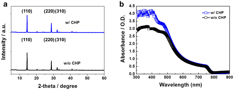
To investigate whether the morphology controller would influence the structural and optical properties of the resulting CH3NH3PbI3 film, we measured the X-ray diffraction (XRD) patterns and UV-vis spectra of the films, as shown in Figure 3. In Figure 3a, the CH3NH3PbI3 films with and without CHP gave quite similar XRD patterns at 14.08°, 28.70°, and 32.12°, corresponding to the (110), (220), and (310) planes, respectively. These three peaks, which originate from the CH3NH3PbI3 crystalline structure19, indicate the high crystallinity of the orthorhombic system. Using these facile and commercially attractive methods (which require only small amounts of additive), the absence of a PbI2 peak in the XRD patterns could be ascribed to the complete consumption of the precursors, comparable to the most reliable methods of vacuum deposition or vapor-assisted solution processing26. In addition, the crystallization of the CH3NH3PbI3 structure without CHP was evaluated, and similar XRD patterns were observed irrespective of the inclusion of the CHP additive.
Figure 3. Characteristics of the CH3NH3PbI3 perovskite thin-film.
(a) XRD patterns and (b) UV-vis spectra of the CH3NH3PbI3 films processed with and without the use of the the CHP additive.
Figure 3b shows the UV-vis spectra of the CH3NH3PbI3 films with and without the CHP additive cast onto glass/ITO/PEDOT:PSS substrates. The remarkable absorption decrease near 500 nm is characteristic of CH3NH3PbI3 films prepared using DMF solvent. As previously reported, CH3NH3PbI3 films have a shoulder band at ~480 nm and onset points near 790 nm that fit into the optical band gap (Eg) of CH3NH3PbI3 perovskite (Eg ≈ 1.5 eV)33,36. In particular, considering that both systems produced a similar film thickness, as discussed in our previous SEM results, the higher absorbance value of the film without CHP longer than 500 nm can be attributed to the formation of pin-holes and to the incomplete coverage of the perovskite film. In contrast, the CHP-based film showed a noise curve in the shorter wavelength than 500 nm which indicated higher optical density than equipmentally detectable value. Considering the similar film thicknesses, the difference in the UV-vis spectra is attributed to the perovskite film morphology19,33. These results are consistent with the SEM results of Figure 2.
Evaluation of photovoltaic performance
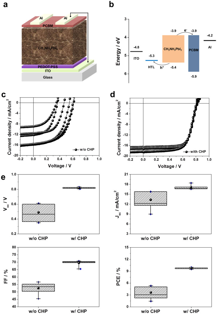
We evaluated the effects of the two different perovskite film morphologies on the cell performances in a device architecture consisting of ITO-coated glass/poly(3,4-ethylenedioxythiophene):poly(styrene sulfonic acid) (PEDOT:PSS) as the anode/hole transport layer, CH3NH3PbI3/(6,6)-phenyl C61-butyric acid methyl ester (PC61BM) as the perovskite planar heterojunction/electron transport layer, and an Al cathode electrode, as shown in Figure 4a. Here, PEDOT:PSS and PC61BM were chosen as the hole and electron transport layers, respectively, as their highest occupied molecular orbital (HOMO) and lowest unoccupied molecular orbital (LUMO) levels match well with the valence and conduction bands of CH3NH3PbI3, which allows for the efficient transport of holes and electrons toward PEDOT:PSS and PC61BM, respectively, as depicted in Figure 4b33,36. Figure 4c–d presents the current density-voltage (J-V) curves of cells prepared with and without the CHP additive, and the corresponding photovoltaic parameters are summarized in Table 1.
Figure 4. Schematics of the device, the photovoltaic performance and statistical analysis of the perovskite solar cells.
(a) Schematic device configuration of the CH3NH3PbI3-based perovskite solar cells and (b) the corresponding energy levels of each layer. The J-V curves of devices made (c) without and (d) with the use of the CHP additive. (e) Statistical analysis of the photovoltaic parameters of the CH3NH3PbI3 perovskite solar cells processed without and with the CHP additive. Note that top and bottom of the boxes is the 75–25 percentile and blue diamond symbols represent outliers in box plots.
Table 1. Summary of the photovoltaic parameters of the CH3NH3PbI3-based perovskite solar cells.
| Condition | Voc/V | Jsc/mAcm−2 | FF/% | PCE/% |
|---|---|---|---|---|
| w/o CHP | 0.49 ± 0.11 | 13.33 ± 2.85 | 52.53 ± 4.05 | 3.63 ± 1.61 (5.34) |
| w/CHP | 0.82 ± 0.01 | 17.10 ± 0.63 | 69.57 ± 1.50 | 9.74 ± 0.14 (10.00) |
Average and standard deviation values were obtained based on 18 cells from 6 different batches. For more accurate reproducibility tests, we fabricated the devices on different substrates and from different casting solutions.
As shown in Figure 4c, the devices without the CHP additive exhibited low performance characteristics: the average open-circuit voltage (Voc) = 0.49 V; the average short-circuit current density (Jsc) = 13.33 mA/cm2; the average fill factor (FF) = 52.53%; and the average PCE = 3.63%. In particular, a large deviation in the Voc and Jsc values, resulting in a wide spread in the device efficiencies, was clearly observed in the J-V curves. It has been proposed that inhomogeneous and incomplete perovskite film morphologies can lead to decreases in Voc and Jsc values due to the formation of low resistance shunting paths and to decreased light absorption in the PeSCs, respectively19,24,33. For these reasons, all photovoltaic parameters of cells without morphology controller showed a large variation, as shown in Figure 4e. In particular, we observed these morphologies in films prepared without the CHP additive (see SEM results of Figure 2) and thus concluded that the poor performance characteristics of the cells with a large device-to-device deviation arose from the undesirable perovskite film morphology.
On the other hand, as observed in Figure 4d, the PeSCs with the CHP additive showed excellent performance characteristics: the average Voc = 0.82 V; the average Jsc = 17.10 mA/cm2; the average FF = 69.57%; and the average PCE = 9.74%. In particular, the best performing device showed a PCE of 10%, a Jsc of 18.39 mA/cm2, a Voc of 0.81 V, and an FF of 67.15%, similar to the values of previously reported high-performance planar or meso-structured PeSCs19,20,26,28,36,37. Furthermore, as shown in Figure 4e, highly reproducible device performances were realized through the use of the CHP additive due to the achievement of fine film morphologies with perfect surface coverage, similar to that of films made by vacuum deposition methods. From these results, it is concluded that the performance as well as the reproducibility of PeSCs is critically affected by the perovskite film quality. Therefore, this new method for realizing uniform and full-coverage perovskite films by using a small amount of CHP as a morphology controller could be a facile way to improve both the efficiency and the reproducibility of PeSCs.
Other additives beside CHP have been tried as shown in Fig. 5. As other candidates, Dimethyl sulfoxide (DMSO, boiling point: 189°C, vapor pressure: 0.6 mmHg) and N-methyl-2-pyrrolidone (NMP, boiling point: 202°C, vapor pressure: 0.3 mmHg), which have higher boiling point and lower vapor pressure at room temperature than DMF solvent (boiling point: 153°C, vapor pressure: 2.9 mmHg) were investigated. As shown in Fig. 5, although DMSO and NMP additive systems exhibited better PCE values than non-additive system, CHP additive system showed much better PCE values than other additive systems. We believe that the reason for the higher performance in the additive systems is derived from the slower crystallization of perovskite layer than DMF-only system due to the lowest vapor pressure of CHP than DMSO and NMP additives.
Figure 5. Maximum PCE of perovskite solar cells with various additives.
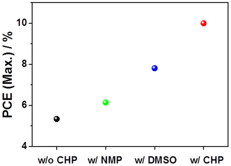
Evaluation of photovoltaic performances without CHP (5.34%), with NMP (6.14%), with DMSO (7.81%), and with CHP (10.00%) from left to right.
Discussion
In summary, we demonstrated high-performance PeSCs with superior reproducibility by incorporating a small amount of CHP additive as a morphology controller into the DMF solution. During film formation using the additive system, the high boiling point and an extremely low vapor pressure of CHP prevented the rapid crystal formation of CH3NH3PbI3 and produced homogeneous nucleation via the remaining CHP in the film, thus producing highly uniform and complete perovskite films similar to those achieved by vapor-deposition method. In this way, the problem of poor morphology can be solved, producing fully covered and highly smooth film morphologies. Using this promising technique, we further demonstrated that a high PCE of 10% as well as superior reproducibility with a performance deviation of 0.14% can be realized. On the basis of our results, we conclude that this new method for realizing efficient and reproducible PeSCs via a morphology controller represents a major step forward for the practical application of PHJ PeSCs because it solves one of the biggest problems of perovskite photovoltaics using a simple processing method.
Methods
Material preparations
All reagents were purchased from Sigma Aldrich and used without further purification. For preparation of the electron transport layer, PCBM (20 mg) was dissolved in anhydrous chlorobenzene (1 ml) at room temperature under constant stirring for 1 h in an N2-filled glove box. For the hole transport layer, commercially available AI 4083 PEDOT:PSS (Baytron P) was used. The CH3NH3I was synthesized according to a previous report33,36.
Fabrication of planar heterojunction PeSCs
ITO-coated glass substrates (18 Ohm/sq, Samsung Corning) were cleaned with de-ionized water, acetone, and isopropyl alcohol in a bath-type sonicator for 10 min each. The cleaned substrates were then dried in an oven at 100°C for 10 min, followed by oxygen plasma treatment for 15 min. The cleaned ITO-coated glass substrates were coated with a thin layer of PEDOT:PSS (~40 nm) fabricated by spin coating, followed by annealing at 110°C for 10 min in air. A perovskite solution composed of a 1:1 molar ratio (CH3NH3I:PbI2 = 0.395 g:1.145 g) dissolved in DMF solvent (2.225 ml) in an N2-filled glove box. Then, 0.95 ml of DMF-only solution was added into 50 μl CHP and the CHP/DMF mixed perovskite solution was deposited on top of the PEDOT:PSS layer for 90 s, followed by annealing at 100°C for 30 s in an N2-filled glove box. For perovskite films containing NMP or DMSO additives, each 50 μl of NMP or DMSO was added to the DMF-only perovskite solution. To form an electron transport layer (~60 nm), a PCBM solution was deposited on the prepared perovskite film at 1000 rpm for 30 s in an N2-filled glove box. Finally, the 100 nm thick Al electrodes were deposited using a thermal evaporator with a deposition rate of 5 Å/s at a pressure of ~10−7 torr.
Device measurement and characterization
The current density-voltage (J-V) characteristics of the CH3NH3PbI3-based cells were measured under simulated AM 1.5G conditions (100 mW/cm2) with a Keithley 2400 instrument calibrated with a Si reference cell (SRC-1000-TC-KG5-N, VLSI Standards. Inc.). (Photovoltaic performances were measured in air without any encapsulation.) UV-vis spectra of the perovskite thin-films were obtained using a Jasco V570 UV-vis/NIR spectrophotometer. The perovskite film morphologies were analyzed using a scanning electron microscope (SEM, HITACHI S-4700). X-ray diffraction (XRD) data of perovskite films were recorded using a Rigaku Micromax-002 diffractometer with CuKα (λ = 0.1542 nm) radiation.
Author Contributions
J.-M.Y., S.-S.K. and D.-Y.K. planned and supervised the project. Y.-J.J. and S.L. designed and performed the experiments. Y.-J.J. and S.L. analyzed and interpreted the data and wrote the manuscript. R.K. and J.-E.Kim interpreted the data. J.-S.Y. and S.-H.L. found the incorrect expressions. J.-M.Y. and S.L. synthesized the CH3NH3I. J.-M.Y. and D.-Y.K. contributed to discussions throughout the project. Y.-J.J. and S.L. contributed equally to this work.
Acknowledgments
This work was supported by the National Research Foundation of Korea(NRF) grant funded by the Korea government(MSIP) (NRF-2010-0029212) and the National Research Foundation of Korea (NRF) grant funded by the Korea government (MSIP) (No. 2012M2A2A6013183).
References
- Sariciftci N. S., Smilowitz L., Heeger A. J. & Wudl F. Photoinduced electron transfer from a conducting polymer to buckminsterfullerene. Science 258, 1474–1476 (1992). [DOI] [PubMed] [Google Scholar]
- Yu G., Gao J., Hemmelen J. C., Wudl F. & Heeger A. J. Polymer photovoltaic cells enhanced efficiencies via a network of internal donor-acceptor heterojucntions. Science 270, 1789–1791 (1995). [Google Scholar]
- Kim M. et al. Electrical performance of organic solar cells with additive-assisted vertical phase separation in the photoactive layer. Adv. Energy Mater. 4, 1300612 (2014). [Google Scholar]
- O'regan B. & Grfitzeli M. A low-cost, high-efficiency solar cell based on dye-sensitized. Nature 353, 737–740 (1991). [Google Scholar]
- Yella A. et al. Porphyrin-sensitized solar cells with cobalt (II/III)–based redox electrolyte exceed 12 percent efficiency. Science 334, 629–634 (2011). [DOI] [PubMed] [Google Scholar]
- Kim H.-S. et al. Lead iodide perovskite sensitized all-solid-state submicron thin film mesoscopic solar cell with efficiency exceeding 9%. Sci. Rep. 2, 591 (2012). [DOI] [PMC free article] [PubMed] [Google Scholar]
- Park N.-G. Organometal perovskite light absorbers toward a 20% efficiency low-cost solid-state mesoscopic solar cell. J. Phys. Chem. Lett. 4, 2423–2429 (2013). [Google Scholar]
- Gevorgyan S. A., Alstrup J. & Krebs F. C. A roll-to-roll process to flexible polymer solar cells: model studies, manufacture and operational stability studies. J. Mater. Chem. 19, 5442–5451 (2009). [Google Scholar]
- Na S.-I., Kim S.-S., Jo J. & Kim D.-Y. Efficient and flexible ITO-free organic solar cells using highly conductive polymer anodes. Adv. Mater. 20, 4061–4067 (2008). [Google Scholar]
- Hou S. et al. Flexible conductive threads for wearable dye-sensitized solar cells. J. Mater. Chem. 22, 6549–6552 (2012). [Google Scholar]
- You J. et al. A polymer tandem solar cell with 10.6% power conversion efficiency. Nat. Commun. 4, 1446 (2013). [DOI] [PMC free article] [PubMed] [Google Scholar]
- Yella A. et al. Molecular engineering of push–pull porphyrin dyes for highly efficient dye-sensitized solar cells: the role of benzene spacers. Angew. Chem. Int. Ed. 126, 3017–3021 (2014). [DOI] [PubMed] [Google Scholar]
- Blom P. W., Mihailetchi V. D., Koster L. J. A. & Markov D. E. Device physics of polymer: fullerene bulk heterojunction solar cells. Adv. Mater. 19, 1551–1566 (2007). [Google Scholar]
- Yanagida S., Yu Y. & Manseki K. Iodine/iodide-free dye-sensitized solar cells. Acc. Chem. Res. 42, 1827–1838 (2009). [DOI] [PubMed] [Google Scholar]
- Chung I., Lee B., He J., Chang R. P. & Kanatzidis M. G. All-solid-state dye-sensitized solar cells with high efficiency. Nature 485, 486–489 (2012). [DOI] [PubMed] [Google Scholar]
- Snaith H. J. Perovskites: the emergence of a new era for low-cost, high-efficiency solar cells. J. Phys. Chem. Lett. 4, 3623–3630 (2013). [Google Scholar]
- Ball J. M., Lee M. M., Hey A. & Snaith H. J. Low-temperature processed meso-superstructured to thin-film perovskite solar cells. Energy Environ. Sci. 6, 1739–1743 (2013). [Google Scholar]
- You J. et al. Low-temperature solution-processed perovskite solar cells with high efficiency and flexibility. ACS nano 8, 1674–1680 (2014). [DOI] [PubMed] [Google Scholar]
- Chen Q. et al. Planar heterojunction perovskite solar cells via vapor assisted solution process. J. Am. Chem. Soc. 136, 622–625 (2014). [DOI] [PubMed] [Google Scholar]
- Heo J. H. et al. Efficient inorganic-organic hybrid heterojunction solar cells containing perovskite compound and polymeric hole conductors. Nat. Photon. 7, 486–491 (2013). [Google Scholar]
- Wojciechowski K., Saliba M., Leijtens T., Abate A. & Snaith H. Sub 150° C processed meso-superstructured perovskite solar cells with enhanced efficiency. Energy Environ. Sci. 7, 1142–1147 (2014). [Google Scholar]
- Xing G. et al. Long-range balanced electron-and hole-transport lengths in organic-inorganic CH3NH3PbI3. Science 342, 344–347 (2013). [DOI] [PubMed] [Google Scholar]
- Stranks S. D. et al. Electron-hole diffusion lengths exceeding 1 micrometer in an organometal trihalide perovskite absorber. Science 342, 341–344 (2013). [DOI] [PubMed] [Google Scholar]
- Eperon G. E., Burlakov V. M., Docampo P., Goriely A. & Snaith H. J. Morphological control for high performance, solution-processed planar heterojunction perovskite solar cells. Adv. Funct. Mater. 24, 151–157 (2014). [Google Scholar]
- Conings B. et al. Perovskite-based hybrid solar cells exceeding 10% efficiency with high reproducibility using a thin film sandwich approach. Adv. Mater. 26, 2041–2046 (2013). [DOI] [PubMed] [Google Scholar]
- Liu M., Johnston M. B. & Snaith H. J. Efficient planar heterojunction perovskite solar cells by vapour deposition. Nature 501, 395–398 (2013). [DOI] [PubMed] [Google Scholar]
- Burschka J. et al. Sequential deposition as a route to high-performance perovskite-sensitized solar cells. Nature 499, 316–319 (2013). [DOI] [PubMed] [Google Scholar]
- Bi D. et al. Using a two-step deposition technique to prepare perovskite (CH3NH3PbI3) for thin film solar cells based on ZrO2 and TiO2 mesostructures. RSC Adv. 3, 18762–18766 (2013). [Google Scholar]
- Liang K., Mitzi D. B. & Prikas M. T. Synthesis and characterization of organic-inorganic perovskite thin films prepared using a versatile two-step dipping technique. Chem. Mater. 10, 403–411 (1998). [Google Scholar]
- Brivio F., Walker A. B. & Walsh A. Structural and electronic properties of hybrid perovskites for high-efficiency thin-film photovoltaics from first-principles. APL Mat. 1, 042111 (2013). [Google Scholar]
- Lee M. M., Teuscher J., Miyasaka T., Murakami T. N. & Snaith H. J. Efficient hybrid solar cells based on meso-superstructured organometal halide perovskites. Science 338, 643–647 (2012). [DOI] [PubMed] [Google Scholar]
- Docampo P., Ball J. M., Darwich M., Eperon G. E. & Snaith H. J. Efficient organometal trihalide perovskite planar-heterojunction solar cells on flexible polymer substrates. Nat. Commun. 4, 2761 (2013). [DOI] [PubMed] [Google Scholar]
- Jeng J. Y. et al. CH3NH3PbI3 perovskite/fullerene planar-heterojunction hybrid solar cells. Adv. Mater. 25, 3727–3732 (2013). [DOI] [PubMed] [Google Scholar]
- Liang P.-W. et al. Additive enhanced crystallization of solution-processed perovskite for highly efficient planar-heterojunction solar cells. Adv. Mater. 26, 3748–3754 (2014). [DOI] [PubMed] [Google Scholar]
- Xiao M. et al. A fast deposition-crystallization procedure for highly efficient lead iodide perovskite thin-film solar cells. Angew. Chem. 126, 10056–10061 (2014). [DOI] [PubMed] [Google Scholar]
- Sun S. et al. The origin of high efficiency in low-temperature solution-processable bilayer organometal halide hybrid solar cells. Energy Environ. Sci. 7, 399–407 (2014). [Google Scholar]
- Noh J. H. et al. Nanostructured TiO2/CH3NH3PbI3 heterojunction solar cells employing spiro-OMeTAD/Co-complex as hole-transporting material. J. Mater. Chem. A 1, 11842–11847 (2013). [Google Scholar]


