Abstract
Germanium-based materials and device architectures have recently appeared as exciting material systems for future low-power nanoscale transistors and photonic devices. Heterogeneous integration of germanium (Ge)-based materials on silicon (Si) using large bandgap buffer architectures could enable the monolithic integration of electronics and photonics. In this paper, we report on the heterogeneous integration of device-quality epitaxial Ge on Si using composite AlAs/GaAs large bandgap buffer, grown by molecular beam epitaxy that is suitable for fabricating low-power fin field-effect transistors required for continuing transistor miniaturization. The superior structural quality of the integrated Ge on Si using AlAs/GaAs was demonstrated using high-resolution x-ray diffraction analysis. High-resolution transmission electron microscopy confirmed relaxed Ge with high crystalline quality and a sharp Ge/AlAs heterointerface. X-ray photoelectron spectroscopy demonstrated a large valence band offset at the Ge/AlAs interface, as compared to Ge/GaAs heterostructure, which is a prerequisite for superior carrier confinement. The temperature-dependent electrical transport properties of the n-type Ge layer demonstrated a Hall mobility of 370 cm2/Vs at 290 K and 457 cm2/Vs at 90 K, which suggests epitaxial Ge grown on Si using an AlAs/GaAs buffer architecture would be a promising candidate for next-generation high-performance and energy-efficient fin field-effect transistor applications.
Shrinking the feature size of silicon (Si) metal-oxide-field-effect transistors (MOSFETs) has enabled the doubling of transistor densities every two years1,2 and has been central to the realization of cost-effective and powerful computing systems. Further downscaling of Si nanoscale transistor size for performance per function and lower supply voltage operation for lower dynamic/leakage power faces three critical issues: i) lower supply voltage leads to an increase in the leakage current of a transistor that degrades the switching current ratio between the ON and OFF states, ii) lower operating electric field results in lower carrier velocity and hence, less transistor ON current, and iii) lower gate voltage swing available to turn-off the transistor results in increased leakage power. Monolithic heterogeneous integration of new materials and novel device architectures on Si are required to continue transistor miniaturization and enable low-power (<0.5 V) transistor operation in order to reduce power consumption. One attractive approach is changing the transistor design, from planar to fin field-effect transistors (FinFETs), where the “fin” design allows the gate to control the channel from three sides as opposed to one3. Utilizing the benefits of high hole mobility along two (110) Ge sidewall surfaces, the FinFET design allows for the continued scaling of operating voltages below 0.5 V while maintaining transistor performance. Due to the increased electron and hole mobility, as compared to Si, Ge is an attractive candidate for the future generation of high-performance, low-power and high-speed nanoscale logic transistors.
While attempts have been made to obtain high-performance transistors using bulk Ge4,5,6, Ge directly deposited on Si7,8, Ge on graded Si1-xGex buffers9,10, Ge-on-insulator-on-Si (GeOI) by wafer bonding11, and compressively strained Ge quantum well on Si12, all of these methods have failed to achieve a high valence band offset required for carrier confinement to the active Ge channel, and elimination of parallel conduction within the buffer layer. There are no prior reports on the heterogeneous integration of epitaxial Ge on Si, through the use of a large bandgap III–V buffer architecture for FinFET applications where the epitaxial Ge thickness is the fin height. In order to achieve device-quality Ge epilayers on such a buffer, careful design of the various aspects of the buffer growth must be considered, including: i) buffer architecture selection and its impact on defect and dislocation propagation, ii) lattice-matched or strained Ge epilayer selection and its influence on fin height, and iii) valence band offset selection and its influence on carrier confinement within the active Ge epilayer. In this paper, we demonstrate an Si-compatible heterogeneous integration process of device-quality and low dislocation density epitaxial Ge layer on Si using a composite AlAs/GaAs metamorphic buffer, grown using solid source molecular beam epitaxy (MBE), and further, we comprehensively investigate the surface and interface properties, band alignment properties, and electrical transport properties of this structure. This study shows the suitability of the AlAs/GaAs metamorphic buffer approach for epitaxial Ge on Si by evaluating the band alignment properties at the Ge/AlAs heterointerface. The valence and conduction band discontinuities, ΔEV and ΔEC, at the Ge/AlAs heterojunction were larger than 0.5 eV and 1 eV, respectively, which is sufficient to serve as a blocking barrier for holes as well as a blocking barrier for electrons, in low-power device applications, i.e. if the driving voltage of the transistor is less than 0.5 V. Another fascinating role of the large bandgap AlAs buffer layer is to prevent a parallel conduction path to the active Ge channel, thus enabling an increase in transistor ON current when used in Ge FinFET device architectures. Moreover, the larger bandgap AlAs layer, when compared to GaAs13, will provide a higher ΔEV and hence increased carrier confinement in the active Ge layer. The importance of using wide bandgap materials for the buffer layer lies in reducing the residual carrier concentration, providing a high resistivity buffer for device isolation and reduced junction leakage, minimizing dislocation density at the end of buffer grading and virtual substrate formation, and maintaining a smooth surface template for active layer growth. In the past, Ge/AlAs or Ge/GaAs semiconductor heterojunctions and their band alignments have been of considerable interest14,15,16. Integrated on an Si substrate using a large bandgap buffer, they could enable the monolithic integration of electronics and photonics.
Structural analysis
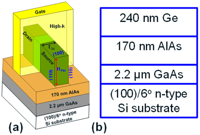
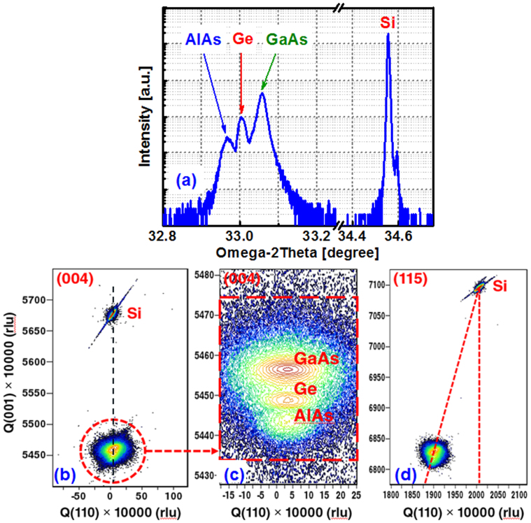
Figure 1a, b presents a schematic illustration of a 3-dimensonal Ge vertical FinFET device on an Si substrate using an AlAs/GaAs metamorphic buffer architecture, and the layer structure used for this study, respectively. The structural quality and the relaxation state of the 240 nm Ge/170 nm AlAs/2.2 μm GaAs/Si structure were evaluated using a high-resolution (004) x-ray rocking curve as shown in Fig. 2a, the structure of which is shown in Fig. 1b. The peak positions of Ge, AlAs, GaAs and the Si substrate are clearly visible in this figure. The angular separation, Δθ, between the (004) diffraction peaks of GaAs and Si resulting from the difference in lattice plane spacing Δd/d shows the full relaxation of the GaAs layer, which can serve as a “virtual” substrate for epitaxial Ge growth. Moreover, both the AlAs and Ge peak positions with respect to GaAs are indicative of the lattice matched nature of the layer structure, as expected. The entire layer structure was further investigated by triple axis x-ray diffraction measurements by collecting both (004) and (115) reciprocal space maps (RSMs), which can provide the perpendicular and parallel lattice constants of each layer, highlight defect induced broadening or mosaic spread, quantify the lattice tilt due to misfit dislocations, identify the degree of film relaxation, and precisely determine the position of each layer along the omega axis. The (004) RSM exhibited two distinct reciprocal lattice point (RLP) maxima corresponding to the Si substrate and the Ge/AlAs/GaAs epilayer, as shown in Fig. 2b. Precisely tuning the scan range of the triple axis diffractometer to match that of the epilayer peak positions allowed in the de-convolution of the individual epilayer peaks, i.e., the RLPs of Ge, AlAs, and GaAs shown in Fig. 2b become separate contours of intensity as shown in Fig. 2c. The intensity of the AlAs contour is lower due to the thickness of this layer used for this study. Figure 2d shows the (115) RSM of this structure where the Ge/AlAs/GaAs RLPs follow the relaxed line as indicated in the figure, implying that the buffer layer, AlAs/GaAs as well as the epilayer Ge are fully relaxed with respect to the Si substrate. The degree of relaxation of the Ge epilayer was evaluated by measuring the perpendicular lattice constant from (004) and the parallel lattice constant from (115) and it was found to be less than 5% with respect to the GaAs “virtual” substrate, owing to the lattice matching of the AlAs and GaAs layers. Such minimal relaxation is expected due to the quasi-lattice matched nature (~0.07% lattice mismatch) of the Ge/GaAs heterostructure. Furthermore, there is a minimal lattice tilt observed from the (004) RSM, as shown by a vertical line in the figure, which implies that the buffer layer, AlAs/GaAs and the Ge epilayer surfaces were parallel to the surface of (100)/6°-offcut Si substrate. The minimal lattice tilt aids prospective device engineering, allowing for the design of the carrier transport direction in future FinFET devices based on such material systems.
Figure 1. Schematic cross-section of the (a) Ge based nanoscale fin field-effect transistor structure on Si using a composite AlAs/GaAs metamorphic buffer architecture where the thickness of the Ge layer is the fin height and (b) the layer structure studied in this paper.
Figure 2. X-ray diffraction analysis of Ge on Si: (a) X-ray rocking curve from the 240 nm thick Ge grown on an Si substrate using an AlAs/GaAs buffer, (b) symmetric (004) reciprocal space map of the Ge/AlAs/GaAs/Si structure, (c) reciprocal lattice point of GaAs, Ge and AlAs layer precisely determined using triple axis proportional detector, and (d) asymmetric (115) reciprocal space map of the structure.
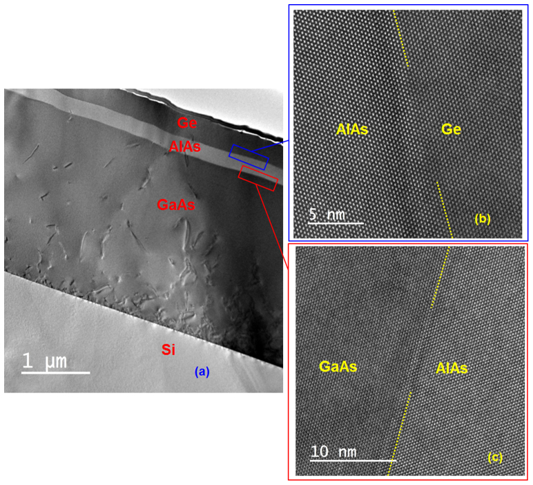
The structural quality and the defect properties of the structure were examined by cross-sectional transmission electron microscopy (TEM). Figure 3a shows the cross-sectional bright field TEM micrograph of the entire layer structure, showing the interfaces between Ge and AlAs, AlAs and GaAs, and GaAs and Si. The image of Fig. 3a shows a high contrast at each interface and the observed threading dislocation density (TDD) decreases along the growth direction, indicating that the bulk of the dislocations were confined within ~0.5 μm of the GaAs buffer layer. Beyond this region, the TDD decreases abruptly due to annihilation of dislocations with opposite Burgers vectors resulting in a “virtually” dislocation-free Ge channel layer. It can be also seen that the composite AlAs/GaAs buffer layer effectively accommodates the lattice mismatch between the active Ge layer and the Si substrate. The composite buffer provided a high-quality “virtual” substrate platform for the active Ge layer, which could be used to fabricate Ge-based FinFET devices. Further investigation of the Ge layer and each heterointerface was performed by recording high-resolution TEM micrographs of each interface. The relative long range uniformity of each interface is visible in the high-resolution TEM micrographs of the Ge/AlAs and AlAs/GaAs heterojunctions, as shown in Figures 3b and 3c, respectively. As shown in Fig. 3c, the active Ge channel layer is lattice matched with the AlAs metamorphic buffer and the lattice line is extended from the Ge layer to AlAs layer. No dislocations were observed at the heterointerface as well as within the Ge layer at this magnification, suggesting the lattice matched nature of the Ge, which is consistent with the results from the XRD analysis. The results from the TEM analysis indicate the high-quality of the film with atomic smoothness reflecting the overall defect-free active Ge channel layer. The TDD of this Ge layer is <107 cm−2 at this magnification. This optimization of the growth parameters in conjunction with the atomic scale imaging is a significant advancement towards demonstrating the correlated synthesis – structure – property behavior. The Ge layer in this structure can be used as the “fin” in a next-generation FinFETs, where the 240 nm Ge thickness serves as the fin height. Moreover, in the next generation nanoscale Ge FinFET transistor structure, a smooth and uniform AlAs layer is essential. This AlAs layer can also be used as an etch stop layer for fabricating nanoscale Ge FinFETs. In conjunction with the absence of defects inside the Ge layer at this scale (Fig. 3b, c), the intended property such as, the band alignment and the electrical transport properties, was obtained.
Figure 3.
Cross-sectional TEM micrographs: (a) Cross-sectional TEM micrograph of the entire Ge/AlAs/GaAs/Si structure, high-resolution TEM micrograph of (b) Ge/AlAs and (c) AlAs/GaAs heterointerfaces. Sharp heterointerfaces between Ge/AlAs and AlAs/GaAs were demonstrated.
Band alignment properties
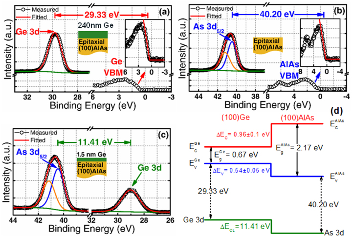
Quantification of the energy band alignment at the Ge/AlAs heterojunction is indispensable since a sufficient barrier for holes and electrons is needed for carrier confinement. The valence band offset, ΔEv, at the Ge/AlAs heterointerface was measured using x-ray photoelectron spectroscopy (XPS) to collect core level (CL) spectra and angle integrated photoelectron energy distribution curves for the valence band maxima (VBM). Using these methods, Ge 3d and As 3d CL spectra were recorded and the binding energy was corrected by adjusting the carbon 1 s CL peak position to 285.0 eV for each sample surface. Figures 4a, 4b, 4c, and 4d show XPS spectra of (a) Ge 3d core level  and VBM
  from a thick Ge epilayer, (b) As 3d
  core level and VBM
  from a thick AlAs layer, (c) Ge 3d core level and As 3d core level spectra from the interface of ~1.5 nm Ge on AlAs, and (d) the corresponding band alignment of the Ge/AlAs heterointerface, respectively. The Ge layer was thinned down carefully by a combination of wet etching and in-situ sputtering performed during the XPS measurement in order to acquire a precise signal from the Ge/AlAs interface. The ΔEv for the Ge/AlAs heterojunction was determined using the measured CL spectra from the following equation17,
 |
Figure 4. Band offsets using x-ray photoelectron spectroscopy: XPS spectra of (a) Ge 3d core level  and valence band maximum, VBM
  from thick Ge film, (b) As 3d
  core level and VBM
  from thick AlAs film, (c) As 3d, Ge 3d core levels from ~1.5 nm Ge/AlAs interface, and (d) energy-band alignment of the Ge/AlAs heterointerface, respectively.
Finally, the conduction band offset, ΔEc, for the Ge/AlAs heterojunction was calculated using the following equation,  , where
  and
and  are the bandgaps of AlAs and Ge, respectively. Using these measured data and the equation above, the measured value of ΔEv for Ge on AlAs was found to be 0.54 ± 0.05 eV and the calculated ΔEc was found to be 0.96 ± 0.05 eV, using the 2.17 eV bandgap of AlAs and 0.67 eV bandgap of Ge. We have carefully analyzed the interface between the AlAs and the Ge layer using high-resolution TEM, and have approximated the intermixing at the heterointerface to be 1.0–2.0 monolayers (ML). Although the atomic arrangement at this interface is not known experimentally, the microscopic arrangement of atoms in the 1.0–2.0 ML transition layer might affect the value of valence band offset. It has been reported18,19 that the interdiffusion affects the band offset modification at semiconductor heterojunctions and it was found that the ΔEv increases with the intermixing of 1.0 ML and then decreases with 2.0 ML of intermixing. In fact, the interdiffusion makes for a smooth interface, rather than an abrupt heterointerface, and resulting from interdiffusion, the ΔEv should reduce the barrier for carrier transport. In our case, the intermixing is about 1.0–2.0 ML and thus, the measured ΔEv in this present work is in the lower limit. Hence, these band alignment values are important design parameters for Ge-based nanoscale transistors at 0.5 V operation.
Electrical transport properties
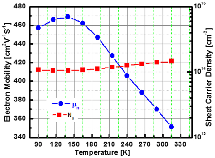
To further investigate the device-quality of the epitaxial Ge film on Si using an AlAs/GaAs composite buffer, the carrier mobility of the Ge film was measured using Hall measurement by the Van der Pauw method in a temperature range from 90 K to 315 K. Figure 5 shows the Hall mobility and carrier density as a function of measurement temperature. The Hall effect measurements were carried out to assess the quality and control of doping in the semiconductor layer with the Hall mobility as an important figure-of-merit. Additionally, the Hall mobility and the sheet carrier density as a function of measurement temperature are the most important design parameters for next generation nanoscale transistors. It is important that carrier freeze-out is minimal at lower temperatures, otherwise, the device will be normally ON during room temperature operation. The Hall mobility was measured to be ~370 cm2/Vs at 290 K for a sheet carrier concentration (n-type) of 1.4 × 1014 cm−2 and approximately 457 cm2/Vs at 90 K for a sheet carrier concentration of 1.1 × 1014 cm−2. This room temperature mobility value is in agreement with the Ge film grown on a (100)/2° GaAs substrate also utilizing a 170 nm AlAs buffer layer. The high mobility of Ge at this doping concentration on an Si substrate can be explained by a low dislocation density inside the Ge layer, which is supported by our structural results.
Figure 5. Hall mobility measurement: Hall mobility and the sheet carrier density as a function of the measurement temperature from 90 K to 315 K.
The mobility values are comparable with the bulk mobility values of Ge at this measured carrier concentration.
Discussion
In summary, the heteroepitaxial integration of Ge on Si using a large bandgap intermediate composite metamorphic AlAs/GaAs buffer architecture by solid source MBE opens up the opportunity for a new class of nanoscale transistors. We demonstrate that the GaAs, Ge and AlAs epilayer peaks were well defined, suggesting the suitability of epi-Ge as a channel material in next generation fin field-effect transistors heterogeneously integrated onto Si. Sharp heterointerfaces between the epitaxial Ge, AlAs, and the GaAs layers were achieved on Si. The valence band offset, ΔEV = 0.54 ± 0.05eV and conduction band offset, ΔEC = 0.96 ± 0.05eV were demonstrated at the Ge/AlAs heterointerface. Although band alignments of Ge/SiGe12 and Ge/Si12 have been reported for 0.5 V transistor operation, it is important to modulate and increase the valence band offset between Ge and the bottom barrier material (e.g., AlAs) in order to increase the carrier confinement inside the Ge channel. Here, we demonstrate a ΔEv of 0.54 eV at the Ge/AlAs heterointerface, which is almost 2× higher than the ΔEv of Si/Ge system12. Hall mobilities of greater than 370 cm2/Vs at 290 K were obtained from a 240 nm thick Ge layer at a ~1 × 1014 cm−2 sheet carrier density with minimal carrier freeze out at 90 K, demonstrating the effectiveness of the AlAs metamorphic buffer underneath the Ge layer grown on Si. The temperature dependent mobility peaked at about 125 K, with the mobility values comparable with those of bulk Ge for a similar doping concentration. This further demonstrates the effectiveness of the composite metamorphic buffer on Si, thereby paving the way for designing Ge-based nanoscale fin transistors and photonic devices.
Methods
Material Synthesis
The undoped epitaxial 80–240 nm thick Ge layers were grown using an in-situ growth process on GaAs and Si substrates using separate solid source molecular beam epitaxy growth chambers for the Ge and III–V materials, connected via an ultra-high vacuum transfer chamber. The growth temperature and growth rate of epitaxial Ge were 400°C and 0.1 Å/s, respectively. The details of the epitaxial Ge growth procedure on GaAs are reported elsewhere13. The GaAs nucleation and the buffer layer were grown on (100) Si substrates that are 6° off towards [110] direction using a two-step growth processes: i) low temperature <450°C and low growth rate 0.25Å/s and ii) high temperature ≥600°C and high growth rate 2.5 Å/s. The low temperature growth creates two-dimensional growth and the high temperature growth reduces the dislocations due to the lattice mismatch between the GaAs and the Si substrate. After the growth of the GaAs layer, a lattice matched large bandgap 170 nm AlAs layer was grown at a growth temperature of ≥600°C. After the growth of the AlAs layer inside the III–V compound semiconductors MBE chamber, the sample was cooled down to below 200°C. Thereafter, the AlAs/Ge/Si sample was transferred to a separate MBE growth chamber for Ge growth using an ultra-high vacuum transfer chamber ~5 × 10⁻¹⁰ torr. The base pressure of the Ge chamber was 4–5 × 10⁻¹¹ torr and ~2.4 × 10⁻⁹ torr during the Ge growth at 400°C at a growth rate of 0.1Å/s. After the Ge layer growth, the sample was slowly cooled down at 5°C/min ramp rate to prevent thermal cracking of the structure.
Microscopic and band alignment measurements
To determine the structural quality and the relaxation state of epitaxial Ge on Si using a composite AlAs/GaAs buffer layer, high-resolution triple axis x-ray rocking curves and reciprocal space maps were recorded by a Panalytical XpertPro system using both PIXel and proportional detectors. Cross-sectional high-resolution transmission electron microscopy (HR-TEM) was used to characterize the entire layer structure on Si and each interface. HR-TEM imaging was performed using a JEOL 2100 transmission electron microscope. For this purpose, the electron transparent foils of thin film cross-sections of Ge/AlAs/GaAs/Si were prepared by a standard polishing technique, i.e. mechanical grinding, dimpling and low temperature (~150 K) Ar+ ion beam milling. The band alignment between the Ge and AlAs layers was investigated using a PHI Quantera SXM XPS system with a monochromatic Al-Kα (energy of 1486.7 eV) x-ray source. The Ge 3d and As 3d5/2 core level (CL) binding energy spectra as well as Ge and As valence band binding energy spectra were collected with a pass energy of 26 eV and an exit angle of 45°. The binding energy was corrected by adjusting the carbon 1 s CL peak position to 285.0 eV for each sample surface. Curve fitting was performed by CasaXPS 2.3.14 using a Lorentzian convolution with a Shirley-type background. The CL energy position was defined to be the center of the peak width at half of the peak height. The VBM values were determined by linear extrapolation of the leading edge to the base line of the valence band spectra recorded for the 240 nm Ge and 170 nm AlAs layers. The VBM value is sensitive to the choice of points on the leading edge used to obtain the regression line. The uncertainty of ΔEv and ΔEc values were found to be in the range of 0.05–0.1 eV by the regressions analysis of selected data over the linear region.
Carrier transport measurement
Au/Ti (600Å/200Å) ohmic contacts required for the Hall mobility measurements were made on Ge/AlAs/GaAs/Si in a Kurt J. Lesker PVD 250 physical vapor deposition system. The four corner contacts were defined using positive photoresist and prebaked at ~85°C prior to the deposition of Au and Ti metals. The deposited contacts were annealed at 350°C for 4 minutes under a mixture of N2∶H2 (95∶5 volume ratio). The carrier density and the Hall mobility were measured as a function of temperature from 90 K to 315 K with a fixed magnetic field of 0.55T using an Ecopia HMS5000 Hall measurement system.
Author Contributions
M.H. conceived and supervised the research and helped Y.Z. and N.J. for epitaxial Ge growth on Si using AlAs/GaAs buffer. Y.Z. performed the x-ray measurement. M.C. performed the XPS measurement and data analysis. N.J. performed the Hall mobility measurement as a function of temperature. P.G. prepared the TEM sample and performed the imaging. M.H. wrote the paper. All authors discussed the results and commented on the manuscript.
Acknowledgments
This work is supported in part by Intel Corporation and National Science Foundation under grant number ECCS-1348653. Y. Z. acknowledges the financial support from NSF under grant number ECCS-1028494. P. G. acknowledges support from the National Science Foundation Graduate Research Fellowship under Grant Number DGE 0822220. The authors would like to acknowledge Dr. Niloy Mukherjee at Intel Corporation for technical discussion. The authors would also like to acknowledge NCFL-Institute for Critical Technology and Applied Sciences (ICTAS) and Virginia Tech Nanofabrication Facilities for materials characterization.
References
- Moore G. No Exponential is Forever: But “Forever” Can Be Delayed!. Solid-State Circuits Conference, 2003. Digest of Technical Papers. ISSCC. 2003 IEEE International 10-13 Feb. 2003, San Francisco, CA, IEEE, pp. 20–23 (2003) (10.1109/ISSCC.2003.1234194). [Google Scholar]
- International Technology Roadmap for Semiconductors. (2013); http://www.itrs.net/Links/2013ITRS/2013Chapters/2013PIDS_Summary.pdf (05/10/2014).
- Kavalieros J. T. et al. Tri-Gate Transistor Architecture with High-k Gate Dielectrics, Metal Gates and Strain Engineering. International Symposium on VLSI Technology, Systems, and Applications pp. 50–51 (2006). Honolulu, HI; IEEE (10.1109/VLSIT.2006.1705211); June 13th, 2006. [Google Scholar]
- Heyns M. et al. Advancing CMOS beyond the Si roadmap with Ge and III/V devices. Electron Devices Meeting (IEDM), 2011 IEEE International, 5–7 Dec. 2011, Washington, DC, IEEE, pp. 13.1.1–13.1.4 (2011) (10.1109/IEDM.2011.6131543). [Google Scholar]
- Mitard J. et al. Record ION/IOFF performance for 65 nm Ge pMOSFET and novel Si passivation scheme for improved EOT scalability. Electron Devices Meeting (IEDM), 2008 IEEE International 15–17 Dec. 2008, San Francisco, CA, IEEE, pp. 873–876 (2008) (10.1109/IEDM.2008.4796837). [Google Scholar]
- Zhang R., Iwasaki T., Taoka N., Takenaka M. & Takagi S. High-Mobility Ge pMOSFET with 1-nm EOT Al2O3/GeOx/Ge Gate Stack Fabricated by Plasma Post Oxidation. IEEE Transactions on Electron Devices 59, 335–341 (2012). [Google Scholar]
- Krishnamohan T., Krivokapic Z., Uchida K., Nishi Y. & Saraswat K. C. High-mobility ultrathin strained Ge MOSFETs on bulk and SOI with low band-to-band tunneling leakage: experiments. IEEE Transactions on Electron Devices 53, 990–999 (2006). [Google Scholar]
- Krishnamohan T. et al. High-mobility low band-to-band-tunneling strained-germanium double-gate heterostructure FETs: Simulations. IEEE Transactions on Electron Devices 53, 1000–1009 (2006). [Google Scholar]
- Ho B., Nuo X. & Tsu-Jae King L. pMOSFET performance enhancement with strained Si1-xGex channels. IEEE Transactions on Electron Devices 59, 1468–1474 (2012). [Google Scholar]
- Chleirigh C. N. et al. Thickness dependence of hole mobility in ultrathin SiGe-channel p-MOSFETs. IEEE Transactions on Electron Devices 55, 2687–2694 (2008). [Google Scholar]
- Hutin L. et al. GeOI pMOSFETs scaled down to 30-nm gate length with record off-state current. IEEE Electron Device Letters 31, 234–236 (2010). [Google Scholar]
- Pillarisetty R. et al. High mobility strained germanium quantum well field effect transistor as the p-channel device option for low power (Vcc = 0.5 V) III–V CMOS architecture. Electron Devices Meeting (IEDM), 2010 IEEE International 6–8 Dec. 2010, San Francisco, CA, IEEE, pp. 6.7.1–6.7. 4 (2010) (10.1109/IEDM.2010.5703312). [Google Scholar]
- Hudait M. K., Zhu Y., Jain N. & Hunter J. L. Jr Structural, Morphological, and Band Alignment Properties of GaAs/Ge/GaAs Heterostructures on (100), (110), and (111)A GaAs Substrates. Jr. J. Vac. Sci. Technol. B 31, 11206–11219 (2013). [Google Scholar]
- Franciosi A. & Van de Walle C. G. Heterojunction band offset engineering. Surf. Sci. Reports 25, 1–140 (1996). [Google Scholar]
- Van de Walle C. G. & Neugebauer J. Universal alignment of hydrogen levels in semiconductors, insulators and solutions. Nature 423, 626–628 (2003). [DOI] [PubMed] [Google Scholar]
- Yu E. T., Mccaldin J. O. & Mcgill T. C. Band Offsets in Semiconductor Heterojunctions. Solid State Physics 46, 1–146 (Academic, Boston, 1992). [Google Scholar]
- Kraut E. A., Grant R. W., Waldrop J. R. & Kowalczyk S. P. Precise Determination of the Valence-Band Edge in X-Ray Photoemission Spectra: Application to Measurement of Semiconductor Interface Potentials. Phys. Rev. Lett. 44, 1620–1623 (1980). [Google Scholar]
- Rodriguez-Hernandez P., Mujica A. & Munoz A. Interdiffusion effects in the band offset modification by intralayer deposition at semiconductor homojunctions. Physica B 185, 546–550 (1993). [Google Scholar]
- Biasiol G. et al. A. Microscopic capacitors and neutral interfaces in III–V/IV/III–V semiconductor heterostructures. Phys. Rev. Lett. 69, 1283–1286 (1992). [DOI] [PubMed] [Google Scholar]


