Abstract
This report is to address the question if black γ-polymorph of cesium tin tri-iodide (B-γ-CsSnI3) can be used as a solid-state hole-transport material in the conventional DSSCs with the N719 dye to replace the liquid electrolyte as reported by I. Chung et al. on Nature 485, 486, (2012). Here we demonstrate rigorously that B-γ-CsSnI3 is not energetically possible to collect photogenerated holes because of the large energy barrier at the interface of N719/B-γ-CsSnI3. Therefore, it cannot serve as a hole-transporter for the conventional DSSCs although it is a good hole-conducting material. A solution-based method was employed to synthesize the B-γ-CsSnI3 polycrystalline thin-films used for this work. These thin-films were then characterized by X-ray diffraction, Hall measurements, optical reflection, and photoluminescence (PL). Particularly, spatially resolved PL intensity images were taken after B-γ-CsSnI3 was incorporated in the DSSC structure to insure the material integrity. The means of ultraviolet photoemission spectroscopy (UPS) was used to reveal why B-γ-CsSnI3 could not act as the substitute of liquid electrolyte in the conventional DSSCs. For the completeness, other two related compounds, one is the yellow polymorph of CsSnI3 and other is Cs2SnI6 with tetravalent tin instead of double-valent tin in CsSnI3 were also investigated by UPS.
Over the last a few years, a rapid progress has been made on the power conversion efficiency (PCE) of the Gratzel type of solar cells by making use of low-cost, solution-processable perovskite semiconductors1,2,3,4,5,6,7,8. It was recently reported to be 15.4% for the CH3NH3PbI3 based Gratzel solar cells8, widely expected to be improved further and possibly exceeding 20% in near future, hence challenging the mature crystalline-silicon based solar cell technology. Although the perovskite material itself is relatively inexpensive, the reported devices7,8 commonly use an expensive organic hole-transport polymer, called spiro-OMeTAD, which has a commercial price that is more than 10 times that of gold or platinum. Several attempts have been made to discover other hole-transporters; most noticeable one was reported by In Chung et al.9 in which they claimed B-γ-CsSnI3 could be used as hole-transporting material in the conventional dye-sensitized DSSCs with the N719 dye. Their devices had an efficiency of 10.6% along with other improvements. CsSnI3 is a perovskite semiconductor10. If their claim could be rigorously verified, it would infer a great possibility of fabricating high performance perovskite based solar cells all by low-cost solution processes. Many research groups have been working hard to confirm their results; it apparently is fraught with many difficulties. In this communication, we demonstrate that B-γ-CsSnI3 is not possible to collect photogenerated holes energetically. Therefore, it cannot serve as a hole-transporter in the conventional DSSCs using the N719 dye as an absorption material, although it is generally a good hole-conducting material. With a motivation of verifying if B-γ-CsSnI3 can be served as a hole-collector as well as a hole-transporter, a reliable process is used to fabricate the conventional DSSCs with an obtainable PCE of 7.1%. A low-cost and solution-based method is then employed to synthesize B-γ-CsSnI3 thin-films. These thin-films are then characterized by X-ray diffraction (XRD), Hall measurements, and optical reflection, and PL spectroscopy before they are used to replace liquid electrolyte in DSSCs. Particularly, spatially resolved PL intensity images of photo-anode are used to insure the material integrity after B-γ-CsSnI3 has been blended into the DSSC structure (TiO2/N719/B-γ-CsSnI3). Ultraviolet photoemission spectroscopy (UPS) is used to manifest why B-γ-CsSnI3 cannot energetically collect the photogenerated holes generated in the N719 dye. To eliminate the possibility of B-γ-CsSnI3 being transformed into other compounds when it is blended into DSSCs, two related compounds, one is the yellow polymorph of CsSnI3 (Y-CsSnI3) and other is Cs2SnI6 with tetravalent tin instead of double-valent tin as in CsSnI3, are also investigated by UPS.
Results
XRD data of B-γ-CsSnI3, Y-CsSnI3, and Cs2SnI6
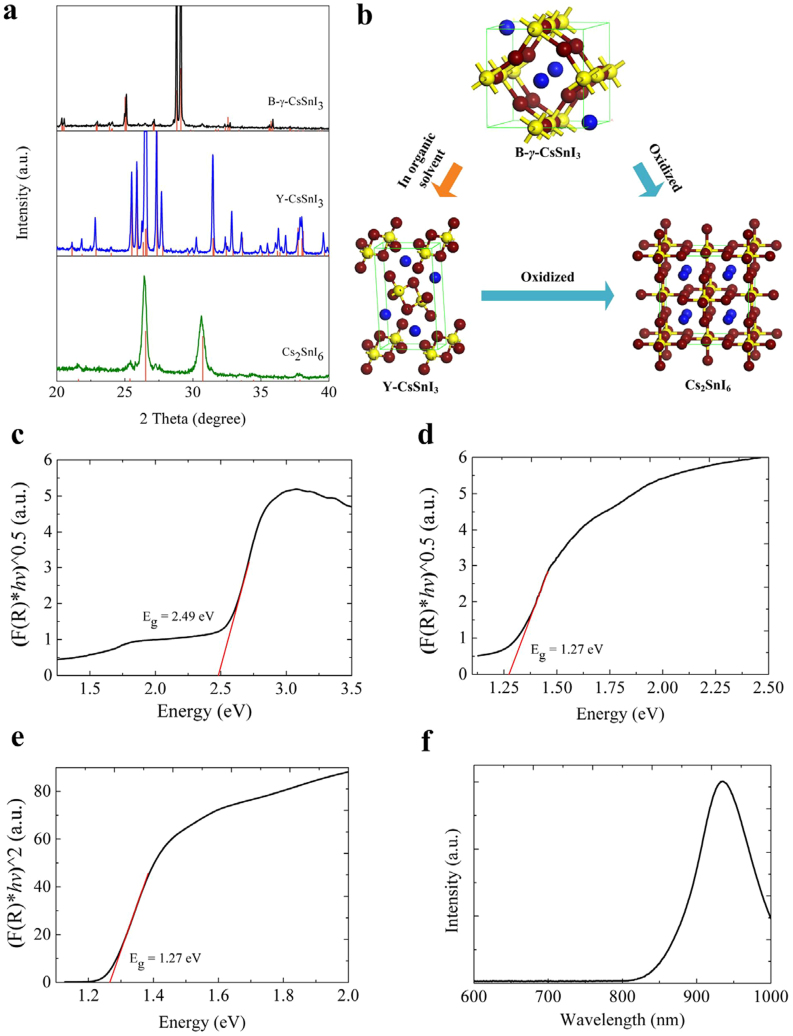
Figure 1 (a) shows the XRD patterns of B-γ-CsSnI3, Y-CsSnI3, and Cs2SnI6, from the top to bottom panel, respectively. It is shown that all of the characteristic XRD peaks match well to the theoretically generated positions and related strengths shown as straight lines for B-γ-CsSnI3, Y-CsSnI3, and Cs2SnI6. This match validates the simple solution method used to synthesize B-γ-CsSnI3 and other relevant methods to produce yellow polymorph of CsSnI3, Y-CsSnI3, and Cs2SnI6. It is generally known, however, that B-γ-CsSnI3 is not stable; when it is exposed to organic solvents; it undergoes a reconstructive phase transition to Y-CsSnI3 at room temperature. When B-γ-CsSnI3 or Y-CsSnI3 is being exposed to air, it will be oxidized in terms of tin atom and becomes Cs2SnI6. The atomic structures and relationship of the three related compounds are displayed in Figure 1 (b).
Figure 1. Atomic Structures and optical properties of B-γ-CsSnI3, Y-CsSnI3 and Cs2SnI6.
(a) The XRD patterns of B-γ-CsSnI3, Y-CsSnI3, and Cs2SnI6. (b) Schematic representation of the phase changing processes from B-γ-CsSnI3 to Y-CsSnI3 and then to Cs2SnI6, red balls present “I”, yellow balls present “Sn”, and blue balls stand for “Cs”. (c), (d) and (e) are UV-vis absorption spectra of Y- CsSnI3, Cs2SnI6, and B-γ-CsSnI3, respectively. (F(R)*hν)α is proportional to absorption coefficient, where F(R) is the Kubelka-Munk function of reflection spectrum, R(v). The exponent, α, is equal to 2 and 0.5 for direct and indirect band-gap semiconductor, respectively. (f) The PL spectrum of B-γ-CsSnI3 thin-film at room temperature.
Optical properties of B-γ-CsSnI3, Y-CsSnI3, and Cs2SnI6
The optical properties of B-γ-CsSnI3 were initially reported by K. Shum et al.10. It possesses a direct energy band-gap which was verified experimentally by the photoluminescence spectroscopy and theoretically by the first-principles calculations. The Kubelka-Munk analysis of the measured reflection spectrum from the synthesized thin-film yields an optical band-gap of 1.27 eV at room temperature, which is consistent with the reported value. Based on the first-principles simulations, Y-CsSnI3 and Cs2SnI6 are indirect band gap semiconductors. Their band gaps are 2.49 and 1.27 eV, respectively using the Kubelka-Munk analysis as shown in Figure 1 (c), and (d), respectively.
Electrical properties of B-γ-CsSnI3, Y-CsSnI3, and Cs2SnI6
In order to determine the unintentionally doped carrier density and type of B-γ-CsSnI3, Y-CsSnI3, and Cs2SnI6 in their thin-film format synthesized by the solution method, a Hall sample holder with flat top was designed and fabricated, which contains Ti pads embedded in SiO2 on Si substrate. The Hall data for a batch of B-γ-CsSnI3 samples with three thicknesses are summarized in the Table 1. The data consistently show that the B-γ-CsSnI3 semiconductor thin-film is of p-type with the carrier concentration of ~ 1019 cm−3. The mobility of holes at room temperature increases from ~ 3 to 20 cm2V−1s−1 as the film thickness increases from 150 to 600 nm. The unintentionally doped carrier density and type for Y-CsSnI3 and Cs2SnI6 thin-films are not determined due to the limited sensitivity of our Hall measurement apparatus.
Table 1. Summary of the Hall data taken from a batch of B-γ-CsSnI3 samples.
| Thickness (nm) | Mobility (cm2V−1s−1) | Carrier Density (1019cm−3) | Conduction Type |
|---|---|---|---|
| 150 | 2.66 ± 0.66 | 4.10 ± 0.27 | p |
| 300 | 4.78 ± 0.59 | 4.17 ± 0.17 | P |
| 600 | 19.59 ± 4.05 | 3.05 ± 0.53 | p |
Uniformity and quality examination of B-γ-CsSnI3 which has been infiltrated into photoanode
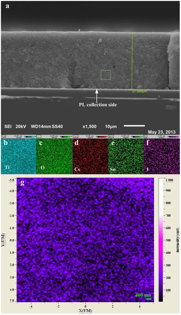
Since B-γ-CsSnI3 is subject to the structural change and oxidation when it is being exposed to air, it is essential to check the uniformity and quality of B-γ-CsSnI3 when it has been infiltrated into the nano-crystal layer of photoanode. This is being done by the energy dispersive spectroscopy in which individual atomic element can be mapped and by the photoluminescence spectroscopy by which the polycrystalline quality of B-γ-CsSnI3 can be characterized. Figure 2 (a) shows the cross-sectional scanning electron microscopy (SEM) image of the photoanode, with a thickness of ~ 27 micrometers. The element of Ti, O, Cs, Sn, and I were mapped out as shown in Figure 2 (b), (c), (d), (e), and (f), respectively. These element maps indicate that all three elements contained in B-γ-CsSnI3 are homogeneously permeated deep into the photoanode. In order to insure that the material infiltrated with the TiO2 nano-crystal network is indeed high quality polycrystalline B-γ-CsSnI3. A spatially resolved PL at the characteristic emission wavelength of B-γ-CsSnI3 at 950 nm was measured from the back side of the photoanode as shown in Figure 2 (g). This two-dimensional PL intensity image demonstrates that the spin-coated B-γ-CsSnI3 uniformly infiltrates into the nano-porous network of TiO2 layer and dose not turn to Y-CsSnI3 or Cs2SnI6 during the material processing.
Figure 2. Structural and material characterization of the B-γ-CsSnI3 coated photoanode (glass/TiO2/N719/B-γ-CsSnI3).
(a) Cross-sectional SEM image of the B-γ-CsSnI3 coated photoanode. The material uniformity is shown by the elemental mapping images of (b), (c), (d), (e), and (f) for Ti, O, Cs, Sn, and I atoms, respectively. (g) Spatially resolved PL centered at 950 nm emitted from B-γ-CsSnI3.
After the verification of uniformity and quality of B-γ-CsSnI3, a complete batch of DSSC devices filtrated with B-γ-CsSnI3 were tested under the photoexcitation power density of 100 mW per cm2 (AM 1.5). The measured I-V curves for all the tested devices in several batches show straight lines and pass though the zero point of the I-V coordinate, indicating the devices lack of photovoltaic effects.
UPS spectra of B-γ-CsSnI3, Y- CsSnI3, and Cs2SnI6
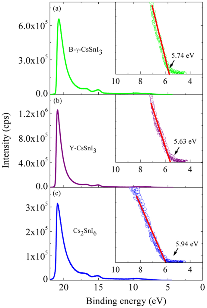
In order to resolve the discrepancy between our experimental results and the published results by Chung et al.9,11, we rely on the UPS method to accurately determine the position of valence band maximum, EVB, of B-γ-CsSnI3, which can directly reveal whether B-γ-CsSnI3 can collect the photogenerated holes in the N719 dye. It should be mentioned here that B-γ-CsSnI3 was determined as a p-type semiconductor in the bulk format by Chung et al.9 and confirmed by our work as described in this work in the thin-film format. Therefore, there is no question about whether B-γ-CsSnI3 is a good hole-conducting material or not. Figure 3 (a) shows the UPS spectrum of B-γ-CsSnI3, where the energy axis is calibrated with respect to the He-I photon energy of 21.21 eV. From this spectrum, the EVB of B-γ-CsSnI3 is determined to be −5.74 eV below the vacuum level which is different from the value of −4.92 eV claimed by the previous report9. With the energy band-gap of B-γ-CsSnI3, Eg = 1.27 eV as determined by the UV-vis reflection spectrum as shown in Figure 1 (e), the conduction band edge, ECB, in reference to the vacuum level for B-γ-CsSnI3 is located at −4.47 eV. In addition, the UPS spectra of Y-CsSnI3 and Cs2SnI6 have been taken and their values of EVB are indicated in Figure 3 (b) and (c), respectively.
Figure 3. UPS spectra of B-γ-CsSnI3, Y-CsSnI3, and Cs2SnI6.
As indicated in the insets, the value of EVB for B-γ-CsSnI3 Y-CsSnI3, Cs2SnI6 are – 5.74, - 5.63, and - 5.94 eV in reference to the vacuum level, respectively.
Determination of the HOMO and LUMO energy levels of the N719 dye
Figure 4 (a) shows the measured UPS pattern of N719. The HOMO energy level (vs vacuum) of N719 is −5.34 eV and the band gap is 2.33 eV as estimated from the UV-Visible absorption spectrum shown in Figure 4 (b). According to the values of HOMO and band gap, the LUMO energy level (vs vacuum) of N719 is −3.01 eV. In addition, the HOMO level was also measured electrochemically via cyclic voltammetry (CV) with ferrocence/ferrocenium (Fc/Fc+) as the internal standard, by using the onset potential of the first oxidation peak. Figure 4 (c) illustrates the CV scans of N719 with dimethylformamide (DMF) as a solvent. The onset potential of oxidation for N719 was measured to be 0.66 V (vs Ag/AgCl), corresponding to 0.57 V (vs Fc/Fc+). The HOMO level for N719 was then estimated to be −5.37 eV (vs vacuum) on the basis of a stable oxidation potential of −4.8 eV (below vacuum level) for Fc/Fc+. This value is in agreement with the value determined by the UPS method.
Figure 4. Experimental determination of the HOMO and LUMO energy levels of the N719 dye.
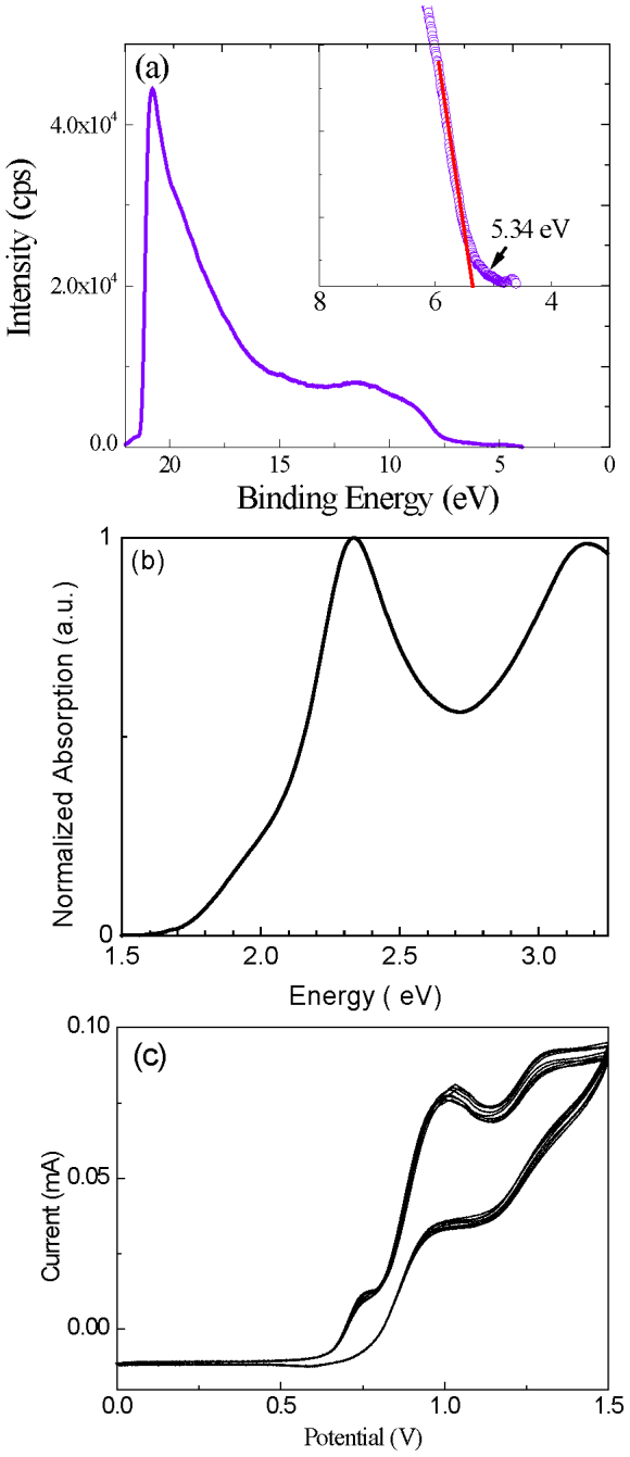
(a) UPS pattern of N719 indicating the HOMO energy level of −5.34 eV below the vacuum level, (b) Normalized UV-visible absorption spectrum of N719 in ethanol which provides an estimation of the band gap of N719, and (c) Cyclic voltammograms of the N719 dye in DMF measured at a scan rate of 50 mV/s.
Discussion
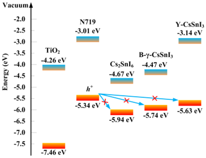
The UPS spectra of B-γ-CsSnI3, Y-CsSnI3, and Cs2SnI6 were measured from three batches of fresh samples to enhance the accuracy of extracted values of EVB. With the consideration of measurement variations, the EVB values for B-γ-CsSnI3, Y-CsSnI3, and Cs2SnI6 are −5.74 ± 0.12, −5.63 ± 0.08, and −5.94 ± 0.04 eV, respectively. To insure the consistency, the values of HOMO and LUMO for the N719 dye, were also measured by the UPS method to be −5.34 and −3.01 eV, respectively. These values were also experimentally confirmed by the CV measurements. They are in agreement with the reported values in the literature12,13. Figure 5 shows the energy band alignments of the TiO2, N719, B-γ-CsSnI3, Y-CsSnI3, and Cs2SnI6. Three conclusions can be drawn by inspecting this figure. First, there is a well-established energy barrier with a value of 0.40 eV at the interface of N719-dye and B-γ-CsSnI3. This value is much larger than the UPS experimental variations and can be considered to be reliable. With this large energy barrier, the photogenerated holes in the N719 dye cannot be collected into B-γ-CsSnI3, revealing the reason why the photovoltaic effects were absent in the TiO2/N719/B-γ-CsSnI3 structured DSSCs as described in the last section. Second, it is not possible to consider B-γ-CsSnI3 in the reported DSSCs by Chung et al.9 might be transformed to Y-CsSnI3 or Cs2SnI6 since the energy barriers at the interface of N719/Y-CsSnI3 and N719/Cs2SnI6 are 0.29, 0.60 eV, respectively, as also illustrated in Figure 5. Third, the value of HOMO for most dyes are below −5.5 eV, therefore, it is unlikely B-γ-CsSnI3 can be considered as a suitable candidate to replace the electrolyte in conventional DSSCs.
Figure 5. Energy band alignments of the TiO2, N719, B-γ-CsSnI3, Y-CsSnI3, and Cs2SnI6.
The energy barrier between N719 and B-γ-CsSnI3 is 0.40 eV, the photogenerated holes in the N719 dye are energetically impossible to be collected by B-γ-CsSnI3 as indicated by a red cross.
Methods
Method of synthesizing B-γ-CsSnI3, Y-CsSnI3, and Cs2SnI6
B-γ-CsSnI3 was prepared via a solution method. The CsI powders were first dissolved in N, N-dimethylformamide (DMF) to form a clear transparent solution. The milled SnI2 powders were added in to the CsI solution. The moral ratio of CsI and SnI2 was 1:1, and the concentration was 1 M. The mixed solution was stirred until forming a clear yellow solution which can be considered as the precursor solution of B-γ-CsSnI3. Finally, the precursor solution was spin-coated to a substrate and dried at 80°C, B-γ-CsSnI3 with metallic luster was formed. Y-CsSnI3 was transformed from B-γ-CsSnI3 in absolute ethanol. The B-γ-CsSnI3 powders were put in absolute ethanol and stirred until becoming a bright yellow suspension. The suspension was then dried at 50°C to remove absolute ethanol and Y-CsSnI3 poly-crystallites remained. All above process must be carried out under protection of N2 in a glove box with the water vapor and oxygen content under 1 ppm. To synthesize the Cs2SnI6 compound, B-γ-CsSnI3 or Y-CsSnI3 was placed in a drying oven in air; either of them would gradually turn to black Cs2SnI6.
Method of fabricating the conventional DSSCs with PCE > 7% as a reference platform
SnO2:F (FTO) transparent conducting oxide coated glasses were used as the electrode for collecting electrons. A thin TiO2 blocking layer was fabricated by spin-coating TiO2 sol onto the FTO substrate, and then dried at 80°C. The complex materials of the TiO2 sol consist of four components partitioned as follows14: Ti[(CH2)3CH3]4 : H2O : HCl : CH3CH2OH = 1 : 4 : 0.15 : 50. The P25 (TiO2) nano-particle paste was prepared as described in the literature15. The fabricated paste was screen printed onto the TiO2 blocking layer on the FTO substrate with an active area of 0.25 cm2, and then heat-treated at 200°C for 4 h before being calcined at 450°C for 4 h at a heating rate of 5°C/min. The sintered TiO2 mesoporous films deposited on FTO substrates were dyed by dipping in an absolute ethanol solution containing 0.5 mM cis-diisothiocyanato-bis(2,29-bipyridyl-4,49-dicaboxylato) ruthenium(II) bis(tetrabutylammonium) (N719) for 24 h at room temperature, followed by rinsing with ethanol and drying. The PCE of the DSSCs fabricated using above-described procedures with a traditional liquid electrolyte is above 7%.
Fabrication of the B-γ-CsSnI3 based solid-state DSSCs
Following the conventional DSSCs fabrication processes described in the last section up to the step of fabricating photoanode, then the CsSnI3 precursor solution was spin-coated in the dye adsorbed mesoporous TiO2 thin-film at 3000 r/min for 1 min and dried at 80°C for 30 min to form a network of B-γ-CsSnI3. (B-γ-CsSnI3 thin-films were also deposited by above spin-coating method.) The Pt counter electrodes were obtained by sputtering Pt onto the FTO substrates. The packaging processes of DSSCs described in Ref. 16 were used.
Description of other experimental apparatuses
The structural properties of B-γ-CsSnI3, Y-CsSnI3, and Cs2SnI6 were characterized by using a PANalytical XRD spectrometer (Model EMPYREAN) with Cu Kα radiation and operated at 40 kV and 100 mA from 10 to 80° in 2θ, and the scanning speed was 10° min−1 at a step of 0.02°. The UV-Vis reflection spectra of B-γ-CsSnI3, Y-CsSnI3, and Cs2SnI6 were characterized by ISR-3100 integrating sphere in SHIMADZU UV-3600 UV-VIS-NIR spectrophotometer. The PL spectra were taken from a Nanolog system from Horiba Jobin Yvon using a laser at 532 nm as the excitation source. The Hall data were tested by a HL 5500 Hall system. The morphological property and EDS mapping of photoanode were observed by a Hitachi S-4800 (Hitachi, Japan) field-emission scanning electron microscopy (FE-SEM). The spatially resolved PL intensity image was taken by a LabRam HR 800 laser confocal Raman spectrometer (Horiba Jobin Yvon). The current-voltage curves of DSSCs were recorded by a Keithley 2400 source-measure unit under the photoexcitation power density of 100 mW/cm2 (AM 1.5) using the Newport Solar Simulator. UPS spectra were taken in an ultrahigh vacuum chamber of ESCALAB 250Xi Ver 2 electron energy spectrometer with a base pressure of < 2 × 10⁻⁸ Pa. The samples were cleaned by argon-ion sputtering (2000 eV, 300 sec) to remove the surface contaminants. The excitation source for UPS measurements was He-I emission at 21.21 eV. The overall energy resolution is ~ 0.02 eV. Cyclic voltammetry experiments were carried out by a windows-based electrochemical station (CHI660E) in a three-electrode cell configuration consisting of a platinum working electrode, a platinum counter electrode, and a Ag/AgCl quasi-reference electrode with ferrocence/ferrocenium (Fc/Fc+) as the internal standard using a scan rate of 50 mV/s. The N719 dye was dissolved in DMF with a concentration of 0.01 M. The supporting electrolyte was 0.1 M tetrabutylammonium perchlorate (C16H36NClO4). All of the characterization measurements were carried out at ambient temperature.
Author Contributions
J.Z., Y.R. and K.S. jointly conceived the idea of this study. J.Z. assisted in designing the experiments and in analyzing the experimental data. C.Y. prepared the CsSnI3 precursor solution. L.W. assembled DSSCs. Y.L. performed the characterization experiments. J.Z. prepared the initial manuscript and K.S. revised it. Y.R. and K.S. co-supervised and coordinated this work. All authors discussed the results and commented on the manuscript.
Acknowledgments
This work was partially supported by Chinese Academic Sciences through the Action Plan for Solar Energy program and by New York State Foundation for Science, Technology, and Innovation (NYSTAR) through the Center of Advanced Technology (CAT) at the City University of New York. The work of K. S. was partially sponsored by Sun Harmonics.
References
- Jin H. H. et al. Efficient inorganic–organic hybrid hetero-junction solar cells containing perovskite compound and polymeric hole conductors. Nature photon. 7, 486–491 (2013). [Google Scholar]
- Jun H. N. et al. Chemical management for colorful, efficient, and stable inorganic−organic hybrid nanostructured solar cells. Nano Lett. 13, 1764–1769 (2013). [DOI] [PubMed] [Google Scholar]
- Lee M. M. et al. Efficient hybrid solar cells based on meso-superstructured organometal halide perovskites. Science 338, 643–647 (2012). [DOI] [PubMed] [Google Scholar]
- Ball J. M. et al. Low-temperature processed meso-superstructured to thin-film perovskite solar cells. Energy Environ. Sci. 6, 1739–1743 (2013). [Google Scholar]
- Burschka J. et al. Sequential deposition as a route to high-performance perovskite-sensitized solar cells. Nature 499, 316–319 (2013). [DOI] [PubMed] [Google Scholar]
- Kim H.-S. et al. High efficiency solid-state sensitized solar cell-based on submicrometer rutile TiO2 nanorod and CH3NH3PbI3 perovskite sensitizer. Nano Lett. 13, 2412–2417 (2013). [DOI] [PubMed] [Google Scholar]
- Kim H.-S. et al. Lead iodide perovskite sensitized all-solid-state submicron thin film mesoscopic solar cell with efficiency exceeding 9%. Sci. Rep. 2, 1–7 (2012). [DOI] [PMC free article] [PubMed] [Google Scholar]
- Liu M. et al. Efficient planar hetero-junction perovskite solar cells by vapor deposition. Nature 501, 395–398 (2013). [DOI] [PubMed] [Google Scholar]
- Chung I. et al. All-solid-state dye-sensitized solar cells with high efficiency. Nature 485, 486–489 (2012). [DOI] [PubMed] [Google Scholar]
- Shum K. et al. Synthesis and characterization of CsSnI3 thin films. Appl. Phys. Lett. 96, 221903 (2010). [Google Scholar]
- Chung I. et al. CsSnI3: semiconductor or metal? High electrical conductivity and strong near-infrared photoluminescence from a single material: High hole-mobility and phase-transitions. J. Am. Chem. Soc. 134, 8579–8587 (2012). [DOI] [PubMed] [Google Scholar]
- Hwang S. et al. A highly efficient organic sensitizer for dye-sensitized solar cells, Chem. Commun. 4887–4889 (2007). [DOI] [PubMed] [Google Scholar]
- Angelis F. D. et al. Absorption spectra and excited state energy levels of the N719 Dye on TiO2 in dye-sensitized solar cell models, J. Phys. Chem. C 115, 8825–8831 (2011). [Google Scholar]
- Que W. et al. Thin film TiO2 electrodes derived by sol-gel process for photovoltaic applications. J. Power Sources 159, 353–356 (2006). [Google Scholar]
- Ito S. et al. Fabrication of screen-printing pastes from TiO2 powders for dye-sensitized solar cells. Prog. Photovolt: Res. Appl. 15, 603–612 (2007). [Google Scholar]
- Ito S. et al. Fabrication of thin film dye sensitized solar cells with solar to electric power conversion efficiency over 10%. Thin Solid Films 516, 4613–4619 (2008). [Google Scholar]


