Abstract
Through introducing a probe layer of bis(4,6-difluorophenylpyridinato-N,C2)picolinatoiridium (FIrpic) between QD emission layer and 4, 4-N, N- dicarbazole-biphenyl (CBP) hole transport layer, we successfully demonstrate that the electroluminescence (EL) mechanism of the inverted quantum dot light-emitting diodes (QD-LEDs) with a ZnO nanoparticle electron injection/transport layer should be direct charge-injection from charge transport layers into the QDs. Further, the EL from QD-LEDs at sub-bandgap drive voltages is achieved, which is in contrast to the general device in which the turn-on voltage is generally equal to or greater than its bandgap voltage (the bandgap energy divided by the electron charge). This sub-bandgap EL is attributed to the Auger-assisted energy up-conversion hole-injection process at the QDs/organic interface. The high energy holes induced by Auger-assisted processes can be injected into the QDs at sub-bandgap applied voltages. These results are of important significance to deeply understand the EL mechanism in QD-LEDs and to further improve device performance.
Colloidal quantum dots (QDs) are a favored class of material, since they combine the properties of inorganic semiconductors, such as optical stability, narrow emission linewidth, and mechanical flexibility, with the functional physical properties of conventional inorganic semiconductors1,2,3,4,5,6,7, including solution processability and tunable bandgap. Owing to these unique features, QDs have been actively investigated to utilize in many optoelectronic devices, for example, down-converters in backlit displays8,9, light-emitting diodes (LEDs)10,11,12,13,14, lasers15, photodetectors16 and solar cells17,18,19. Among these potential applications, the high-performance electrically driving QD-LEDs has been of particular interest due to their potential impact on display and lighting technologies. Great effort has been devoted to achieving highly efficient QD-LEDs and there has been numerous progress in improving the device performance by optimizing both QD materials and device architectures20,21. Recently, some record performance parameters for QD-LEDs, such as high external quantum efficiency of approximately 18% and maximum luminance over 200000 cd/m2, have been reported with an inverted device structure14,20. In addition, Auger recombination, one of the most important exciton quenching processes, was also investigated in detail by adjusting the QD structures to explore its effect on the device performance21. The performance of QD-LEDs have been approached to that of organic LEDs (OLEDs) by now22,23. Although the steady and apparent progress — the external efficiency has been increased from less than 0.01% to 18% — in fabrication of efficient QD-LEDs has been reported, the physical nature of electroluminescence (EL) in QD-LEDs, to date, has not been understood clearly. In order to further improve the device performance, much intensive investigation should be deserved to explore the EL mechanism in QD-LEDs.
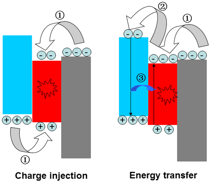
As is well-known, there are two mechanisms proposed to explain the EL processes in QD-LEDs11,12,13. For the first one, carriers transported through charge-transport layers are directly injected into QDs, where they can form excitons that then can radiatively recombine, as shown in Fig. 1 (left panel). The second one depends on the ability to form excitons on the organic molecules surrounding the QD film that then resonantly transfer the exciton energy to QDs. This work mechanism is schematically shown in Fig. 1 (right panel). Hereafter, we refer to the first mechanism as direct charge-injection type (DCI-type) and the second one as energy-transfer type (ET-type). In order to determine the work mechanism in inverted QD-LEDs, the following two demands must be met: (1) the EL must only originates from QDs; (2) the DCI and ET processes can be separately probed, i.e., a delicate design of the QD-LEDs should be implemented to preclude the involvement of these two processes.
Figure 1. The schematic work mechanism in QD-LEDs, direct charge-injection (left) and energy-transfer (right).
 charges injection into QDs,
  electrons injection into HTL, and
  energy transfer from HTL molecules to QDs.
For the inverted QD-LEDs, the DCI-type EL mechanism was proposed in recent reports14,20. But there is not any direct evidence to support this standpoint. In this study, we fabricated a set of inverted QD-LEDs with different thickness neat bis(4,6-difluorophenylpyridinato-N,C2)picolinatoiridium (FIrpic) layers to investigate the work mechanism. In these devices, FIrpic layer is used as a probe layer inserted at the exciton formation interface to monitor the position of exciton formation. The reason of adopting FIrpic as the probe layer is just because of its unique properties, including concentration quenching and similar highest occupied molecular orbital (HOMO) energy level to the hole transport layer (HTL) of 4, 4-N, N- dicarbazole-biphenyl (CBP). Due to the concentration quenching effect, the photoluminescence (PL) yield of neat FIrpic film is decreased by 80% compared to that of optimum guest:host system24. Also, as reported in OLEDs24, the efficiency of OLEDs is dramatically decreased due to the severely exciton quenching with increasing the FIrpic concentration in the host. Thanks to the property of concentration quenching, FIrpic layer at the exciton formation interface can be successfully used to probe the position of exciton formation by comparing the performance of QD-LEDs with and without FIrpic layer. According to our experiment results, the efficiencies of QD-LEDs are only reduced slightly with the introduction of neat FIrpic layer, which indicates that the EL process in our QD-LEDs does not originate from the ET-type mechanism. Otherwise, if the EL mechanism is ET from FIrpic to QDs, thus, the excitons will be first formed on FIrpic and the device efficiency will be dramatically decreased due to the exciton quenching in neat FIrpic layer. At last, the DCI-type mechanism is believed to be responsible to the EL process in the inverted QD-LEDs.
Results
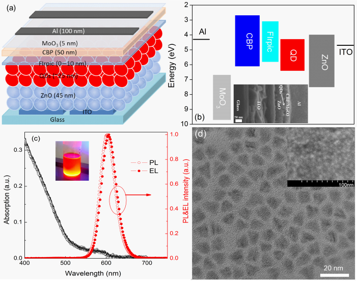
Figure 2a schematically shows the structure of the device with a FIrpic probe layer in the QD-LEDs. The QD emission layer is sandwiched between the ZnO nanoparticle electron transport layer (ETL) and CBP HTL for the control device. The FIrpic layer with different thicknesses is introduced at the QDs/CBP interface to probe the position of exciton formation by assessing the effect of FIrpic layer on device performances. As can be seen from Figure 2b, the exciton recombination zone should be located at QD/CBP or QD/FIrpic interface according to the energy alignment. The inset shows the cross-section SEM image of the device without a FIrpic layer. Figure 2c shows the absorption and PL spectra of the CdSe/CdS/ZnS QDs (in toluene) used in our devices, as well as the EL spectrum of QD-LEDs. The PL emission peak is located at 602 nm and the full-width at half-maximum (FWHM) is 42 nm. We can see that the EL spectrum is almost consistent with the PL one. The FWHM of EL spectrum is also 42 nm with a little redshift of 3 nm compared with the PL one. This well complete PL-EL spectral overlap demonstrates the efficient recombination of holes and electrons on the QDs in the QD-LED. The quantum yield of CdSe/CdS/ZnS QDs is ~60% in solid powder form measured by an integrating sphere. The TEM image of the CdSe/CdS/ZnS QDs is shown in Figure 2d. High crystallinity of individual QDs is obtained and the average diameter of the QDs is ~8.0 nm. The inset shows the top-view SEM image of ITO/ZnO/QDs and we can see the QDs on ZnO film are close-packed.
Figure 2.
(a) The structure schematic diagram of the QD-LEDs in our work. (b) The flat energy levels of the materials used in our study. Inset shows the cross-section SEM image of Device A. (c) The absorption and PL spectra of QDs used in our work. Inset represents the representative UV-illuminated photo of QDs dispersion in toluene. (d) The TEM image of QDs. Inset is the SEM image of sample with a structure ITO/ZnO/QDs.
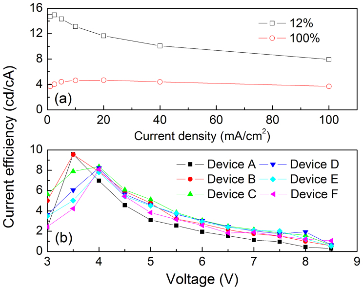
It is well-known that the excitons on QDs can be formed by either DCI into QDs from charge transport layers of ZnO and CBP or ET process from CBP to QDs. In order to determine the EL mechanism in inverted QD-LEDs, one and only method is to distinguish the DCI and ET processes by rationally designing device structure, such as changing the charge transporting layer surrounding the QD layer to adjust the DCI and ET processes. In the control device, replacing the CBP with other common used HTL materials will simultaneously affect the DCI and ET processes from HTL to QDs, by which we cannot precisely evaluate the influence of HTL on the DCI and ET processes. As a result, we cannot determine the EL mechanism in QD-LEDs. To overcome this issue, we insert a phosphorescent small molecule material of FIrpic between QDs and CBP layer due to the unique properties of FIrpic, including concentration quenching and moderate charge injection from FIrpic to QDs. Simultaneously, the ET process from Firpic to QDs is also inefficient as reported by Cheng25. Due to these properties, FIrpic offers a platform to investigate the EL mechanism in inverted QD-LEDs. More specifically, if the EL in the FIrpic-containing QD-LEDs originates from ET process, the device efficiency will be dramatically decreased due to the severe exciton quenching and inefficient ET processes in neat FIrpic layer. In contrary, if the EL mechanism in QD-LEDs is DCI-type, the introduction of FIrpic layer into the devices will have little effect on the efficiency due to the similar HOMO energy levels of CBP and FIrpic as seen in Figure 2b. Firstly, in order to demonstrate the exciton quenching (i.e., the concentration quenching) in neat FIrpic film, the FIrpic based OLEDs with a structure of ITO/PEDOT:PSS/CBP/Emission layer/TPBi/LiF/Al were fabricated. The detailed fabrication procedures are shown in the Methods. The emission layers are composed of CBP:FIrpic (12 wt%) and neat FIrpic for the two OLEDs, respectively. We can see from Figure 3a that the peak efficiency is decreased by 70%, from 15.0 cd/A for CBP:FIrpic based OLED to 4.6 cd/A for neat FIrpic layer based device. These results are in excellent agreement with the discussed in the Introduciton section.
Figure 3.
(a) The current efficiency-voltage characteristics of QD-LEDs; (b) The efficiency-current density curves of FIrpic based OLEDs.
The current efficiency-voltage properties of QD-LEDs with and without a FIrpic probe layer are shown in Figure 3b. As can be seen, the device efficiency is decreased slightly due to the introduction of FIrpic layer. The peak efficiency is decreased from 9.57 cd/A (control device) to 9.55 cd/A (1 nm FIrpic layer), 8.35 cd/A (2 nm FIrpic layer), 8.22 cd/A (5 nm FIrpic layer) 7.80 cd/A (7 nm FIrpic layer) and 8.08 cd/A (10 nm FIrpic layer), which indicates that the influence of FIrpic layer on the device efficiency is insignificant. These results reveal that the EL in these QD-LEDs should dominantly originate from DCI into QDs, not ET process. If the work mechanism in QD-LEDs is ET-type, thus, the excitons will be first formed on FIrpic molecules, then transfer their energy to QDs. According to the discussion above, around 80% of the excitons formed on FIrpic molecules can be quenched24, which will dramatically deteriorate the device performance. But it is not the case. The efficiencies of FIrpic-containing devices are only reduced slightly. For example, the device peak efficiency of Device D (with 5 nm FIrpic layer) is only decreased by less than 14% compared to that of the control device. This is a clear hint that the excitons are directly formed on QDs by DCI process. The larger reduction of efficiency for devices with a thick FIrpic layer should be due to the imbalanced charge injection into the QDs, which will be discussed thereinafter.
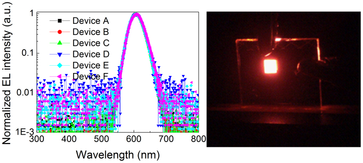
Figure 4 depicts the EL spectra of the QD-LEDs with and without FIrpic layer at an operation voltage of 5 V. Half-exponential coordinates are adopted to clearly exhibit EL components. We can see that the parasitic EL emission from the adjacent organic layers, which commonly occurs in QD-LEDs2, is not observed in our QD-LEDs. The pure QD emission at a peak wavelength of 605 nm with a FWHM of 42 nm illustrates the highly efficient radiative recombination of excitons in the QDs. Moreover, there is not any broadening feature or emission at the low-energy region in the EL spectra for each device, implying absence of emission from deep-level trap states. The EL peak wavelength is red-shifted (~3 nm) relative to the PL emission measured in toluene solution, which may be owing to the dot-to-dot interaction (e.g., Föster resonant energy transfer) in close packed solid films and the Stark effect induced by electric field. All of the results imply that the excitons are dominantly formed on QDs by the DCI processes.
Figure 4.
The left panel represents the EL spectra of QD-LEDs at the operating voltage of 4.5 V. All the EL spectra are shown in a half-exponential coordinates to clearly exhibit EL components; the right panel represents the image of Device B driven under operating voltage of 3.0 V.
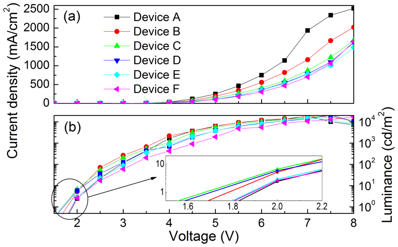
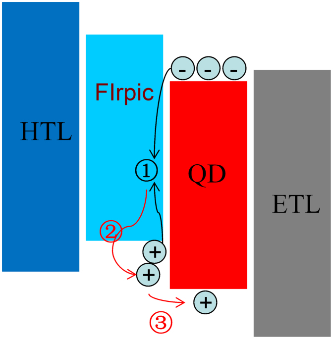
Figure 5a shows the current density-voltage characteristics of the QD-LEDs. The current density is decreased with inserting the FIrpic, the thicker FIrpic, and the larger reduction of current density, which should result from the following two aspects. One is the slightly higher HOMO level of FIrpic than that of CBP; and the other is the lower hole-mobility of FIrpic than that of CBP. These two effects together result in a little larger barrier to hole injection into the QDs than that of device without FIrpic, and hence reducing the current densities of the FIrpic-containing devices. Similarly, the luminance of the QD-LEDs at the same operating voltages is also decreased with increasing the thickness of FIrpic layer as shown in Figure 5b, which is ascribed to the reduction of the injected holes into the QDs. However, an unexpected phenomenon is observed that the turn-on voltage (Vth) is decreased with the introduction of the FIrpic layer. Here, we define the Vth of the QD-LEDs as the voltage at which the luminance of 0.5 cd/m2 was observed. The Vth of all the FIrpic-containing devices is less than that of the control device (1.60 V). The lowest Vth is obtained when the thickness of FIrpic is 2 nm for Device C, which is increased to 1.59 V for Device F with a 10 nm FIrpic layer. In fact, the photon energy of the QDs used in our devices is 2.0 eV, obtained from the PL spectrum peak value of 602 nm. Generally, the Vth should equal to or greater than the bandgap-voltage that is over 2.0 V for the QDs used in our devices. Surprisingly, the turn-on voltages for the QD-LEDs fabricated here are lower than the bandgap-voltage of the QDs. In other words, sub-bandgap driving-voltage QD-LEDs were achieved through an inverted device structure. Similar results were also reported by Mashford et al in the recent publication14, where they attributed this phenomenon to the Auger-assisted charge injection. Here, we illustrate this process in detail as depicted in Figure 6. Under forward bias in the inverted QD-LEDs, holes can be efficiently injected across the MoO3/CBP interface as reported by Lu group26. CBP is a very common hole transport material with a hole mobility of 1.0 × 10⁻³ cm2V−1s−1 and it allows the injected holes to be quickly transported to the CBP/QDs or FIrpic/QDs interface, then accumulated at this interface due to the large energy offset between the HOMO level of CBP (or FIrpic) and the valence band (VB) edge of the QDs (actually, the hole injection barrier between organic layer and QDs is larger than that depicted in Figure 2b due to the wide bandgap ZnS shells and insulated organic ligands outside the QDs). Similarly, electrons are efficiently injected into the conduction band (CB) of the QDs owing to negligible barrier between ZnO and the QDs as shown in Figure 2b. However, the large energy offset of −1.6 eV (~1.2 eV) between the lowest unoccupied molecular orbitals (LUMO) of CBP (FIrpic) and the CB of QDs leads to electron accumulation at the QDs/CBP (or QDs/FIrpic) interface. The electrons and holes form interfacial charge transfer (CT) excitons, or exciplex states upon the accumulation of charges at this interface. The energy relaxed from the recombination of these CT excitons is resonantly transferred to the proximal holes on the CBP (or FIrpic) molecules through an Auger process to produce holes with sufficiently high energy to be injected into the VB of QDs. Then, these injected holes radiatively recombine with the electrons in the CB of the QDs, resulting in emission of photons with energy equal to the badgap of the QDs. According to the Auger-assisted hole-injection mechanism, we can explain that the lower Vth for FIrpic-containing devices is due to the slightly larger barrier to hole-injection at the FIrpic/QDs interface compared to the CBP/QDs interface, which leads to more holes to be accumulated at FIrpic/QDs interface. As we know, a high charge density at the interface is in favor of Auger recombination process.
Figure 5.
(a) The current density-voltage and (b) luminance-voltage characteristics of the QD-LEDs.
Figure 6. The Auger-assisted energy up-conversion process at QD/organic interface:  recombination of interfacial charge transfer (CT) exciton,
  energy transfer from CT exciton to hole, and
  injection of high energy hole across the interface into QDs.
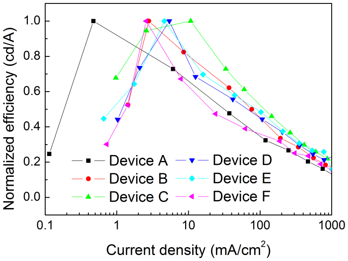
The introduction of FIrpic into the device not only decreases the Vth of the QD-LEDs, but also demonstrates that the concept — inserting a hole block layer to reduce the amount of holes injected into the QDs and consequently improving the charge balance in the QDs — is a good option. As shown in Figure 7, the normalized efficiency is shown as the function of applied current density. The results indicate that the efficiency roll-off of the devices with a FIrpic layer is reduced, which is ascribed to the improved charge balance. The efficiency roll-off of Device F is increased due to the unduly decrease of holes injected into QDs by the thick FIrpic layer, which degenerates the charge balance and efficiency roll-off. Additionally, the peak efficiency of the devices with FIrpic is decreased slightly, which is due to the exciton quenching induced by the accumulated holes at the FIrpic/QDs interface as proposed in our previous report27.
Figure 7. The efficiency versus current density characteristics of the QD-LEDs.
Discussion
Firstly, we present an analysis about the FRET process between the FIrpic molecules and QDs. Then, we discuss the factors limited the device efficiency and the approaches that can be used for obtaining highly efficient QD-LEDs. According to FRET theory, the Förster radius R0 is defined as the separation distance corresponding to 50% FRET efficiency, which can be expressed as:28
 |
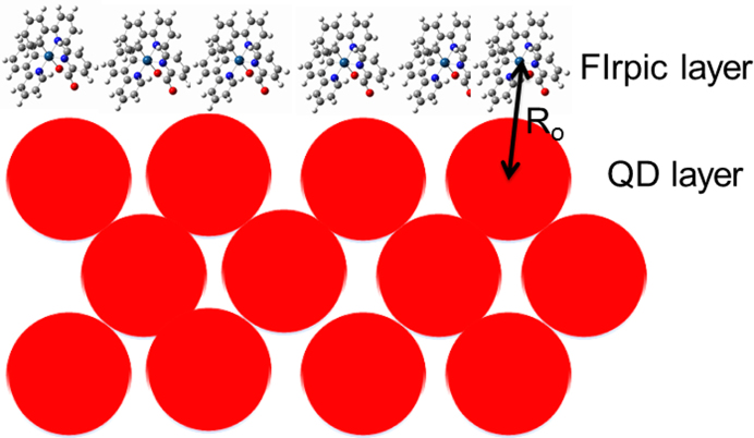
where QD is the quantum yield of the donor, NA is Avogadro's number, nD is the refractive index of the medium and the value of 1.8 is used for organic materials, κ is a parameter that depends on the relative orientation of the donor and acceptor dipoles. We used κ2 = 2/3 here for randomly oriented dipoles. J is the overlap integral. The Förster radius R0 is estimated to be 4.4 nm for FIrpic. As seen from Figure 8, R0 is roughly equal to the center-to-center distance between FIrpic molecule and the proximal QDs, which implies that the excitons formed on FIrpic molecules can be only transferred to the QDs near FIrpic owing to the large size of QDs (8.0 nm in diameter) and the non-planar structure of FIrpic. Therefore, the efficiency of ET from FIrpic to the QDs locating far away from the FIrpic/QDs interface is inefficient and can be negligible. The inefficient ET process will inevitably lead to an emission from FIrpic if the excitons are formed on FIrpic molecules. These results provide an indirect evidence to our standpoints that the work mechanism in inverted QD-LEDs is DCI-type, rather than ET-type.
Figure 8. Schematic packing diagram of FIrpic on QD film.
As proposed in OLEDs and inorganic LEDs, the energy level allignment and charge balance are the most important factors that influence the device performance. The barriers to charge injection into the emission layer are determined by the energy offset between the charge transport layer and QD emission layer. Reducing these barriers will decrease the accumulated charges at the emission heterojunction interfaces, hence widening the exciton recombination zone and decreasing the exciton quenching process, which is beneficial to achieve efficient QD-LEDs and reduce the efficiency roll-off. In addition, the charge balance in the emission layer is another important factor, which limits the device performance. An imbalanced charge injection into the emission layer will lead to a large efficiency roll-off. Balancing the charge (hole and electron) injection by optimizing the device structure and utilizing suitable electron/hole transport layers should be an available approach to improve the performance of the QD-LEDs.
In summary, we have demonstrated, for the first time, the EL mechanism in inverted QD-LEDs by inserting a phosphorescent probe layer of FIrpic between the HTL and QD emission layer. These results reveal that the EL in our inverted QD-LEDs dominantly originates from direct charge-injection into the QDs from the charge transport layer (HTL and ETL layers), but not from the ET process from organic charge transport layers (CBP or FIrpic layer) to QDs. Moreover, EL at sub-bandgap driving voltages was obtained, which is due to the Auger-assisted energy up-conversion hole-injection into the QDs. Our work offers a simple and reliable approach to investigate and understand the EL mechanism in inverted QD-LEDs. These results lay the foundation for rational design of QD-LED structure and further improving the device performances.
Methods
Preparation of CdSe/CdS/ZnS QDs and ZnO nanocarystals
CdSe/CdS/ZnS QDs were synthesized through the method similar to that reported in litherature20. 1 mmol of CdO, 4 mmol of OA and 20 ml of 1-ODE was heated to 300°C under Ar flow in a 100 ml flask. Then, 0.25 mL of TOP dissolving 0.25 mmol Se was injected and the reaction temperature was maintained at 300°C for the CdSe QDs growth with a diameter of 3.0 nm. Then, 0.75 mmol of decanethiol were injected dropwise to form CdS shell (1 nm thickness) on top of CdSe cores. At last, Zn(OA)2 and S dissolved in TBP were sequentially injected into the reactor to form ZnS outer shell (1.5 nm thickness) on top of CdSe/CdS QDs.
ZnO nanoparticles were prepared according to that reported in litherature20. At first, 1.23 g of Zn(Ac)2·2H2O was dissolved in 55 ml of methanol at room temperature. Then, 25 ml of a methanol solution containing 0.48 g of KOH was added dropwise at 60°C with magnetic stirring. The reaction mixture was kept at 60°C for 2 h under Ar atmosphere. The product appeared as white precipitate. After collecting by centrifugation, this white precipitate was washed with methanol. Finally, the precipitate was redispersed in butanol (~25 mg/ml).
Device Fabrication
The QD-LEDs consist of glass coated ITO/ZnO (45 nm)/QDs (~25 nm)/FIrpic (x nm)/CBP (45 nm)/MoO3 (5 nm)/Al (100 nm). The thicknesses of ZnO layer and QD layer is obtained by measuring the cross-section SEM of samples (ITO/ZnO and ITO/ZnO/QDs). The ZnO, QDs, CBP, and MoO3 are used as ETL, emission layer, HTL, and hole-injection layer, respectively. The thickness of FIrpic layer is varied from 0 nm to 10 nm for different devices, Device A (0 nm), Device B (1 nm), Device C (2 nm), Device D (5 nm), Device E (7 nm) and Device F (10 nm). Device A is a control device without the FIrpic interlayer. The organic LEDs with FIrpic as emission layer consist of ITO/PEDOT:PSS (25 nm)/CBP (10 nm)/CBP:FIrpic or neat FIrpic (30 nm)/1,3,5-tris(N-phenylbenzimidazole-2-yl)benzene (TPBi, 50 nm)/LiF(1 nm)/Al(100 nm). Before fabricating the devices, the ITO substrates were ultrasonically cleaned with a standard regiment of acetone, ethanol, deionized water, and isopropanol followed by an ex situ UV ozone treatment in air for 5 min. The ZnO nanoparticles were spin-coated onto the cleaned ITO substrates at 2000 rpm from a 25 mg/ml ZnO butanol solution and then annealed at 150°C for 30 min in a glove box (MBRAUN) to obtain a highly conductive layer with a thickness of about 45 nm. Until the ZnO coating substrates cooling to the room temperature, the QD layer was deposited on ZnO by spin-coating QD toluene solution (5 mg/ml) at 2000 rpm and then annealed at 70°C for 30 min in the same glove box (MBRAUN). The substrates were then quickly loaded into the vacuum chamber and the rest of the device fabrication was finished without breaking vacuum. All films were deposited at pressure below 4 × 10⁻⁶ Torr. Detailed processes of fabrication and measurement for QD-LEDs have been described in our previous papers13,29. CBP, FIrpic, and TPBi were purchased from LumTec and PEDOT:PSS was purchased from H. C. Starck. All the materials were used as received without any further purification. In the same vacuum chamber, the Al cathode lines with a width of 2.5 mm were deposited orthogonally to the 2 mm ITO anode lines to form a 5 mm2 active area.
Sample Characterization
The room temperature absorption spectrum was measured with an ultraviolet/visible spectrometer (UV 1700, Shimadzu) and the PL spectrum of the QDs in toluene was collected by a Hitachi F-4500 spectrophotometer under an excitation wavelength of 400 nm. The transmission electron microscopy (TEM) images were recorded on a Philips TECNAI G2. The morphology of QDs film on ZnO and cross-section image of device A were characterized by scanning electron microscope (SEM) (Hitachi S4800).
Author Contributions
W.Y.J. designed the experiments, analyzed the data, and wrote the manuscript. Q.Z., S.Q. and D.L. assisted in the quantum dot characterization. J.Z., L.Z. and P.J. gave some comments. All authors reviewed the manuscript and discussed the results.
Acknowledgments
This work was supported by the National Natural Science Foundation of China (Nos. 61205025, 11204298, 61275197, 61274126, 51103144, and 11274304), Project supported by State Key Laboratory of Luminescence and Applications, SKKLLA201303 and Hunan Provincial Applied Basic Research Base of Optoelectronic Information Technology, GDXX003.
References
- Brus L. E. Electron electron and electron-hole interactions in small semiconductor crystallites - the size dependence of the lowest excited electronic state. J. Chem. Phys. 80, 4403–4409 (1984). [Google Scholar]
- Colvin V. L., Schlamp M. C. & Alivisatos A. P. Light-emitting-diodes made from cadmium selenide nanocrystals and a semiconducting polymer. Nature 370, 354–357 (1994). [Google Scholar]
- Masumoto Y. & Sonobe K. Size-dependent energy levels of CdTe quantum dots Phys. Rev. B 56, 9734–9737 (1997). [Google Scholar]
- Zhao J., Bardecker J., Munro A., Liu M., Niu Y., Ding I., Luo J., Chen B., Jen A. & Ginger D. Efficient CdSe/CdS quantum dot light-emitting diodes using a thermally polymerized hole transport layer. Nano Lett. 6, 463–467 (2006). [DOI] [PubMed] [Google Scholar]
- Talapin D. V., Lee J., Kovalenko M. V. & Shevchenko E. V. Prospects of colloidal nanocrystals for electronic and optoelectronic applications. Chem. Rev. 110, 389–458 (2010). [DOI] [PubMed] [Google Scholar]
- Bae W. K., Kwak J., Park J. W., Char K., Lee C. & Lee S. Highly efficient green-light-emitting diodes based on CdSe@ZnS quantum dots with a chemical-composition gradient. Adv. Mater. 21, 1690–1694 (2009). [Google Scholar]
- Shen H., Wang S., Wang H., Niu J., Qian L., Yang Y., Titov A., Hyvonen J., Zheng Y. & Li L. S. Highly efficient blue-green quantum dot light-emitting diodes using stable low-cadmium quaternary-alloy ZnCdSSe/ZnS core/shell nanocrystals. ACS Appl. Mater. Interfaces 5, 4260–4265 (2013). [DOI] [PubMed] [Google Scholar]
- Lim J., Jun S., Jang E., Baik H., Kim H. & Cho J. Preparation of highly luminescent nanocrystals and their application to light-emitting diodes. Adv. Mater. 19, 1927–1932 (2007). [Google Scholar]
- Jang E., Jun S., Jang H., Lim J., Kim B. & Kim Y. White-light-emitting diodes with quantum dot color converters for display backlights. Adv. Mater. 22, 3076–3080 (2010). [DOI] [PubMed] [Google Scholar]
- Colvin V. L., Schlamp M. C. & Alivisatos A. P. Light-emitting diodes made from cadmium selenide nanocrystals and a semiconducting polymer. Nature 370, 354–357 (1994). [Google Scholar]
- Dabbousi B. O., Bawendi M. G., Onitsuka O. & Rubner M. F. Electroluminescence from CdSe quantum-dot/polymer composites. Appl. Phys. Lett. 66, 1316–1318 (1995). [Google Scholar]
- Shen H., Lin Q., Wang H., Qian L., Yang Y., Titov A., Hyvonen J., Zheng Y. & Li L. S. Efficient and bright colloidal quantum dot light-emitting diodes via controlling the shell thickness of quantum dots. ACS Appl. Mater. Interfaces 5, 12011–12016 (2013). [DOI] [PubMed] [Google Scholar]
- Ji W. Y., Jing P. T., Zhao J. L., Liu X., Wang A. & Li H. Inverted CdSe/CdS/ZnS quantum dot light emitting devices with titanium dioxide as an electron-injection contact. Nanoscale 5, 3474–3480 (2013). [DOI] [PubMed] [Google Scholar]
- Mashford B. S., Stevenson M., Popovic Z., Hamilton C., Zhou Z., Breen C., Steckel J., Bulović V., Bawendi M., Coe-Sullivan S. & Kazlas P. T. High-efficiency quantum-dot light-emitting devices with enhanced charge injection. Nat. Photon. 7, 407–412 (2013). [Google Scholar]
- Klimov V. I., Mikhailovsky A. A., Xu S., Malko A., Hollingsworth J. A., Leatherdale C. A., Eisler H.-J. & Bawendi M. G. Optical gain and stimulated emission in nanocrystal quantum dots. Science 290, 314–317 (2000). [DOI] [PubMed] [Google Scholar]
- Konstantatos G., Howard I., Fischer A., Hoogland S., Clifford J., Klem E., Levina L. & Sargent E. H. Ultrasensitive solution-cast quantum dot photodetectors. Nature 442, 180–183 (2006). [DOI] [PubMed] [Google Scholar]
- Semonin O. E., Luther J. M., Choi S., Chen H.–Y., Gao J., Nozik A. J. & Beard M. C. Peak external photocurrent quantum efficiency exceeding 100% via MEG in a quantum dot solar cell. Science 334, 1530–1533 (2011). [DOI] [PubMed] [Google Scholar]
- Ning Z., Zhitomirsky D., Adinolfi V., Sutherland B., Xu J., Voznyy O., Maraghechi P., Lan X., Hoogland S., Ren Y. & Sargent E. H. Graded doping for enhanced colloidal quantum dot photovoltaics. Adv. Mater. 25, 1719–1723 (2013). [DOI] [PubMed] [Google Scholar]
- Graetzel M., Janssen R. J., Mitzi D. B. & Sargent E. H. Materials interface engineering for solution-processed photovoltaics. Nature, 488, 304–312 (2012). [DOI] [PubMed] [Google Scholar]
- Kwak J. H., Bae W. K., Lee D. G., Park I., Lim J. H., Park M. J., Cho H. D., Woo H. J., Yoon D. Y., Char K. H., Lee S. H. & Lee C. H. Bright and efficient full-color colloidal quantum dot light-emitting diodes using an inverted device structure. Nano Lett. 12, 2362–2366 (2012). [DOI] [PubMed] [Google Scholar]
- Bae W. K., Park Y.-S., Lim J., Lee D., Padilha L. A., McDaniel H., Robel I., Lee C., Pietryga J. M. & Klimov V. I. Controlling the influence of Auger recombination on the performance of quantum-dot light-emitting diodes. Nat. Commun. 4, 2661 (2013). [DOI] [PMC free article] [PubMed] [Google Scholar]
- Matioli E., Brinkley S., Kelchner K., Hu Y., Nakamura S., DenBaars S., Speck J. & Weisbuch C. High-brightness polarized light-emitting diodes. Light Sci. Appl. 1, e22 (2012). [Google Scholar]
- Xiang C., Koo W., So F., Sasabe H. & Kido J. A systematic study on efficiency enhancements in phosphorescent green, red and blue microcavity organic light emitting devices. Light Sci. Appl. 2, e74 (2013). [Google Scholar]
- Kawamura Y., Goushi K., Brooks J., Brown J. J., Sasabe H. & Adachi C. 100% phosphorescence quantum efficiency of Ir(III) complexes in organic semiconductor films. Appl. Phys. Lett. 86, 071104 (2005). [Google Scholar]
- Cheng G., Lu W., Chen Y. & Che C-M. Hybrid light-emitting devices based on phosphorescent platinum(II) complex sensitized CdSe/ZnS quantum dots. Opt. Lett. 37, 1109–1111 (2012). [DOI] [PubMed] [Google Scholar]
- Liu Z. W., Helander M, G., Wang Z. B. & Lu Z. H. Band alignment at anode/organic interfaces for highly efficient simplified blue-emitting organic light-emitting diodes. J. Phys. Chem. C 114, 16746–16749 (2010). [Google Scholar]
- Ji W. Y., Tian Y., Zeng Q. H., Qu S. N., Zhang L. G., Jing P. T., Wang J. & Zhao J. L. Efficient quantum dot light emitting diodes by controlling the carrier accumulation and exciton formation. ACS Appl. Mater. Interfaces 6, 14001–14007 (2024). [DOI] [PubMed] [Google Scholar]
- Lakowicz J. R. Principles of fluorescence spectroscopy, 3rd ed.(Springer, Berlin, Heidelberg., 2006). [Google Scholar]
- Ji W. Y., Zhang L. T., Gao R. X., Zhang L. M., Xie W. F., Zhang H. Z. & Li B. Top-emitting white organic light-emitting devices with down-conversion phosphors: Theory and experiment. Opt. Express 16, 15489–15494 (2008). [DOI] [PubMed] [Google Scholar]


