Abstract
Deep-ultraviolet surface-enhanced Raman scattering (UV-SERS) is a promising technique for bioimaging and detection because many biological molecules possess UV absorption lines leading to strongly resonant Raman scattering. Here, Al nanovoid substrates are developed by combining nanoimprint lithography of etched polymer/silica opal films with electron beam evaporation, to give a high-performance sensing platform for UV-SERS. Enhancement by more than 3 orders of magnitude in the UV-SERS performance was obtained from the DNA base adenine, matching well the UV plasmonic optical signatures and simulations, demonstrating its suitability for biodetection.
Keywords: resonant Raman, nanobowls, stamps, polymer opals, adenine
Surface-enhanced Raman scattering is a powerful technique to probe small traces of substances via the strong concentration of electric fields on plasmonic substrates. Since its discovery in 1970,1−3 this technique has improved greatly and various plasmonic sensing platforms, ranging from colloidal nanocrystal aggregates4 to nanostructured surfaces5 have demonstrated its usability. To improve the sensitivity further, the most common route is to increase the electromagnetic field intensity in the plasmonic “hot spots”. However, fundamental constraints exist as a result of quantum tunnelling,6 besides the fabrication difficulties at this nanoscale. Another strategy is to identify electronic transitions in the analyte. Tuning the Raman excitation laser to an electronic absorption line increases the Raman scattering cross-section dramatically and leads to resonant Raman scattering, which can be amplified by thousands of times over the nonresonant scattering.7
Existing plasmonic substrates are, so far, mostly limited to the visible spectral range as the typical materials, gold and silver, absorb light at UV frequencies due to interband transitions. However, numerous molecules in biology and chemistry have absorption lines in the UV.8,9 Despite no commercial availability, a reliable sensing platform for this spectral range is highly desirable. Moreover, because 266 nm solid-state sources are becoming widely available, compact, and affordable, this will harness the growing interest in UV SERS.
Previous attempts for near UV-excitation (325 nm) used rhodium (Rh) and ruthenium (Ru)10 with limited success, whereas attempts in the deep-UV (244 nm) are rare. Palladium (Pd)11−13 and aluminum (Al)14−19 have effective plasmonic response in the UV. In particular, Al supports strong plasmons across a broad spectrum ranging from the deep-UV (244 nm) to the NIR, making it a rather universal plasmonic material, as recently demonstrated by Mogensen et al.20 So far, it remains challenging to fabricate colloidal Al nanoparticles (NPs).21−24 Although Al NPs can be formed by annealing Al films, their size distribution is very broad with irregular spacing.25 Using interference lithography, well-defined Al NP patterns can be generated on a developed substrate, which have been utilized as UV SERS substrates.18 However, such methods are expensive and are not scalable. Recently, however, we developed a nanovoid geometry that has been proved to be an excellent SERS substrate due to its effective plasmonic confinement,26,27 and have further shown that Al can be used in nanovoids to get strong enhancement (up to 100-fold) of Raman signals in the UV.16 The fabrication of the nanovoids is however complicated and involves colloidal self-assembly and electrochemical deposition methods. In this case the fabrication of well-ordered colloidal monolayers is particularly challenging as the optimal spheres are <200 nm diameter,28 which requires proper control of the assembly conditions at the air–water interface.16,29,30 It has been difficult to assemble spheres with sizes below 400 nm, as the capillary surface forces between the particles are too weak compared to Brownian motion to form an ordered monolayer at the air–water interface,31,32 and many defects are generated.
In this letter, we propose a facile and cost-effective route, which is suitable for the large scale fabrication of an Al sensing platform for UV-SERS. Large areas of Al nanovoids were fabricated via nanoimprint lithography. Rather than using the traditional self-assembled monolayer as a mask for colloidal lithography, our method starts from the fabrication of the colloidal stamp from polymer opal films (POFs) as shown in Scheme 1. We initially use silica core poly(methyl methacrylate-ethyl acrylate) shell particles (SiO2@PMMA@PEA) to fabricate the POFs using a custom-built roll-and-shear rig.33 Because of the soft and plastic polymeric shells, the hard silica cores rearrange into highly ordered arrays with the assistance of shearing while the polymer shells melt to form a PMMA/PEA matrix. Because the SiO2 sphere arrays are embedded inside this matrix, an additional milling process applied to the POFs can etch away the surface polymer layers to partially reveal the hard silica nanospheres. This highly ordered array of silica spheres in the surface layer is then used as a stamp for imprint lithography. The stamp is here imprinted onto a thin 50 nm film of polystyrene (PS), which is spin-coated on a Si wafer. A layer of 50 nm Al is evaporated onto the nanovoids via E-beam evaporation (Lesker) to form the film of Al nanovoids, which are then ready for further characterization and UV SERS measurement. The skin depth of aluminum in the UV range is <10 nm, so film thicknesses >10 nm support plasmonic activity without attenuation. Larger film thicknesses do not change the plasmonic properties.
Scheme 1. Fabrication Procedure of Al Nanovoids.
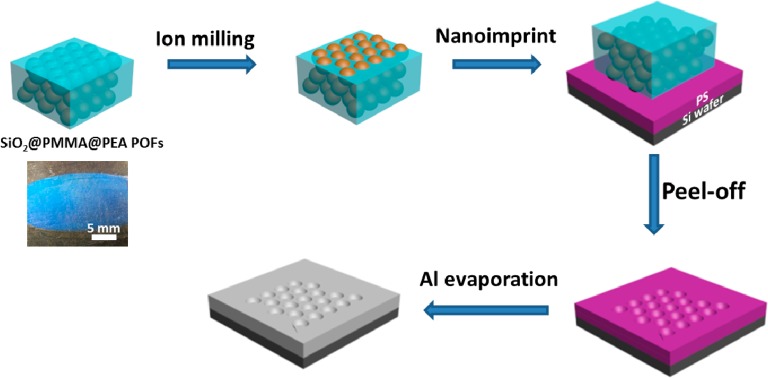
The preformed SiO2@PMMA@PEA opal films were ion-milled, followed by imprinting onto PS films. Al was consequently evaporated on the surface to form Al nanovoids.
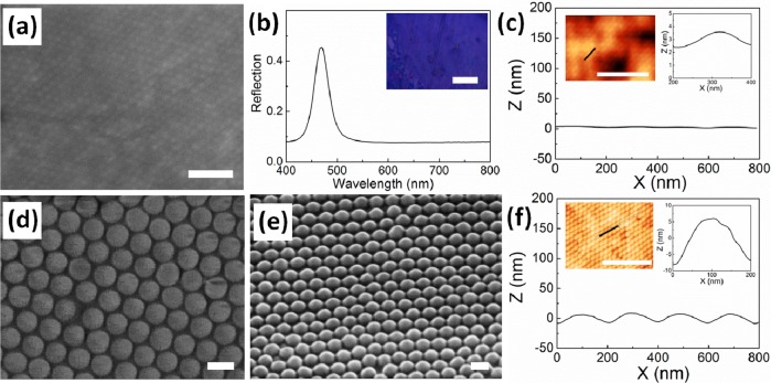
When embedded in the POFs, the morphology of the arrays of silica nanospheres can only be identified with difficulty (Figure 1a). The POFs presents a blue structural color (resonant at 480 nm) with maximum reflectivity of 35% (Figure 1b), which indicates very good ordering of the silica spheres throughout the 3D array. The AFM image (inset of Figure 1c) shows very low contrast because the surface of the POF remains covered with PMMA/PEA although ordered arrays can still be recognized. The height profile of the POF at this stage is very flat with a feature height of only 1–2 nm (right inset of Figure 1c).
Figure 1.
Surface morphology characterization of POFs (a–c) before and (d–f) after ion milling. (a) SEM image of SiO2@PMMA@PEA POFs, scale bar is 1 μm; and (b) the corresponding reflection spectra, inset is the optical image of the POFs, scale bar is 100 μm. (c) AFM characterization of the surface profile of the POFs with AFM image showing in the inset. Scale bar is 2 μm. Right Inset is zoomed region of the surface profile. (d, e) Top and tilted views (0°,30°) of the POFs after 3 min ion milling. Scale bars are 200 nm. (f) Corresponding AFM characterization as c after 3 min ion milling.
There are several routes to remove the polymer layers to reveal the surface profile of the silica spheres. Oxygen plasma cleaning was tested as a convenient way to remove the upper polymer layers on the surface. However, due to heating,34−36 the silica nanospheres were also disordered by the melting and deformation of the polymer as shown in the Supporting Information, Figure S1. Another surface etching technique is ion milling37 where Ar+ ions bombard and decompose the polymers. As this generates less heat the ordering of silica nanospheres is maintained. We therefore chose ion milling to etch away sufficient polymer to enhance the surface profile enough for imprinting. As ion milling also leads to the simultaneous etching of silica nanospheres, we limited the milling time to <4 min at a beam voltage of 500 V, for which the etching of polymer is faster than of silica. The resulted POFs after ion-milling are shown in Figure 1d (top view) and Figure 1e (30° tilted view). The surface morphology of the POFs was composed of partially embedded silica nanospheres with regular spacing, over very larger areas (>1 cm2). The AFM image in the inset of Figure 1f shows much higher image contrast compared to before etching (Figure 1c) and the surface profile shows the expected periodic corrugations of the surface height. The exposed face of the silica nanospheres is around 15 nm in height and 200 nm in diameter (right inset of Figure 1f).
The silica sphere arrays now form a rigid stamp suitable for nanoimprinting, despite their support on the underlying flexible polymer films. Compared to typical nanoimprinting with silica bead arrays in which transfer of the nanoparticles to the imprinted films is often seen, it is not observed here. The sticky layer of PMMA/PEA thus plays a key role in retaining the integrity of silica nanospheres within the POFs during imprinting, and thus the imprinting stamp can be used many times.
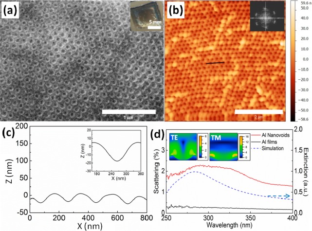
Regular arrays of Al nanovoids are generated after the imprinting and metal coating process (Figure 2a). The AFM image in Figure 2b confirms the ordered arrays of nanovoids with honeycomb-like arrangement, which is the negative print of the silica array on the POF stamp. The height profile in Figure 2c shows a 20 nm maximum depth across the 180 nm diameter of the nanovoids, which almost exactly matches (see the Supporting Information, Figure S3) the feature sizes of the original POF stamp (diameter 200 nm, 15 nm height in crest). Although the short-range order is very good with domain sizes of several microns, the long rang order is interspersed with occasional defects. These defects observable in the AFM image (Figure 2b) are of height ∼30 nm and occur on only <8% of sites introduced during the imprinting process. They originate both from flakes of PMMA/PEA detaching after etching the silica nanospheres in the POF stamps, and from defects of the stamps.
Figure 2.
(a) SEM and (b) AFM images of Al nanovoids. Scale bars are 1 and 2 μm, respectively. The inset in a shows the cm-sized imprinted nanovoid, scale bar is 5 mm. Inset in b is the fast Fourier transfer (FFT) of the AFM image, showing well-defined order. (c) Surface height profile of the nanovoids, inset is zoomed view. (d) Dark field scattering spectra of the Al nanovoids, showing experimental data (red line), simulation (blue dashed), and control for flat Al films (black solid line). Insets are the electric field profile of the Al nanovoids at the spectral peak.
To investigate the plasmonic scattering of the Al nanovoids in the UV spectral range, a dark field scattering measurement rig was constructed (see the Supporting Information, Figure S2). A UV light source is focused through an UV-transparent lens onto the surface of the sample and a 40× reflecting objective (NA = 0.5) collects the scattered light which is directed either to a camera for dark field imaging or to a spectrometer to record the scattering spectra (Figure 2d). A plasmonic-enhanced scattering peak is clearly seen around 290 nm for the films of Al nanovoids (red line), whereas no plasmonic scattering was seen from flat Al films (black line, a zoom-in figure is shown in Figure S4 in the Supporting Information). The simulated spectra (Lumerical FDTD) of Al nanovoids (blue dashed line) shows their first order resonance at 282 nm, which matches well with the experimental data. The additional shoulder around 330 nm in the experimental data likely stems from voids which are closer and plasmonically couple, red-shifting their modes. The optical field distribution on the patterned surface (TE and TM modes in inset of Figure 2d) both show strong electric fields concentrated within the nanovoids, which thus provides an ideal environment for UV-SERS measurements.
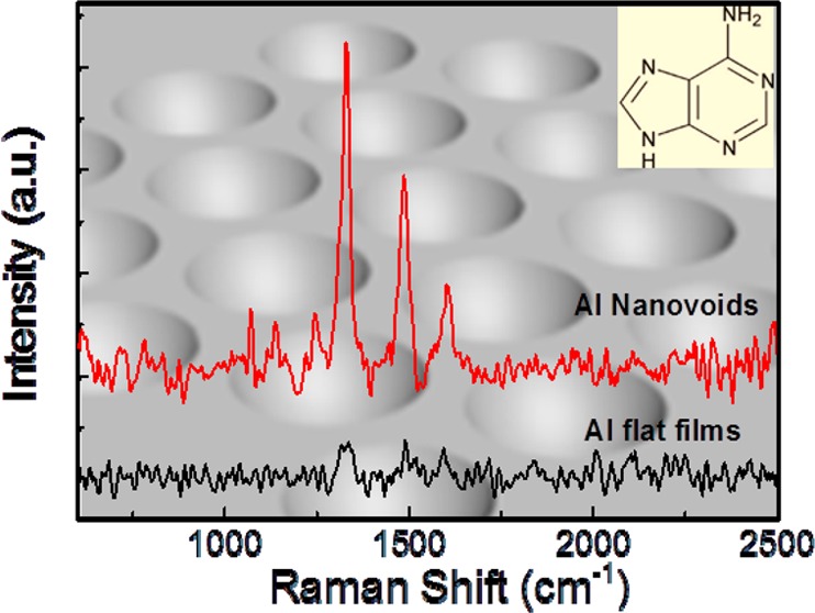
To investigate the potential for UV-SERS, we used adenine as a test molecule. An aqueous solution (1 mM) of adenine was drop-cast onto the nanovoid substrate which was subsequently covered by a quartz coverslip for UV-SERS measurements, forming a thin film of analyte solution on the substrate. The measurements were performed in the solution phase to reduce any molecular degradation, and simulate biochemical sensor conditions. The Raman signal was collected by a Raman system with an excitation laser at 244 nm with total integration time of 30 s (Renishaw). Since higher laser powers induce some photodegradation of the substrate, laser powers below 0.3 mW were used. The UV laser spot diameter was 5 μm. Given the lattice parameter of our array (∼200 nm), we estimate that a typical spectrum contains ∼500 nanovoids. At the pump wavelength (244 nm), both SERS and conventional Raman measurements are in the resonant Raman condition. The SERS enhancement factors quoted below are therefore stated on top of the electronic resonant enhancement. The adenine SERS and Raman spectra (Figure 3a) clearly show the four Raman peaks of adenine (1248, 1332, 1497, and 1620 cm–1) with intensity around 5 counts/mW/s for the 1332 cm–1 peak, while for the flat Al film these peaks are barely seen. Moreover, the UV-SERS signal is highly reproducible across the entire Al nanovoid substrate (see the Supporting Information, Figure S5), which reflects the uniformity of Al nanovoid arrays across the substrate. The relatively larger noise for UV SERS compared with our previous report16 is mainly due to the shorter accumulation time needed to avoid photodegradation of this molecular sample. To further confirm the key contribution from UV resonant plasmons, we checked with excitation wavelengths of 633 nm, and no SERS peaks were observed at all due to excitation far off resonance. The UV-SERS signal of 1 mM adenine obtained from these Al nanovoids is almost of the same intensity as the signals obtained from bulk adenine powder (Figure 3b). The powder form allows the most accurate estimation of the enhancement factors which are rarely stated in the literature in the deep-UV regime. Previous reports for Pd, Rh, and Ru provide only 2 orders of magnitude enhancement factors.10,11 Sigle et al.16 give enhancements of up to 6 orders of magnitude, but this is only given for the hot-spot region rather than averaged over the entire sample. A similar value inside a bow-tie antenna is given by Li et al.17 Here, we state a global enhancement value over the entire sample which we believe is more relevant for a sensing platform. Taking into account the adenine extinction coefficient and the corresponding optical penetration depth in the adenine crystals allows an estimate of the number of molecules in the probe volume. From an adenine extinction coefficient of 1.5 × 10⁴ M–1 cm–1 and molecule diameter of ∼2 nm, we estimate that the number of molecules in the powder form interacting with the laser is ∼4 × 10¹². This can be compared to the number of molecules contributing to the SERS signal (given by the molecular concentration of 1 mM, a void volume of 2 × 10⁶ nm3 and a total number of ∼500 probed voids, which gives 5.9 × 10⁸ molecules contributing to the SERS) and allows determination of the SERS enhancement factor (on top of resonant electronic enhancements always obtained at this wavelength). We estimate this enhancement to be ∼5 × 10³ averaged over the plasmonic surface, which is much higher than previously reported values on such large areas16,18 and is attributed to the near-defect-free fabrication of the surface. These results clearly demonstrate the capability of using aluminum for plasmonic UV-sensing platforms on a large scale.
Figure 3.
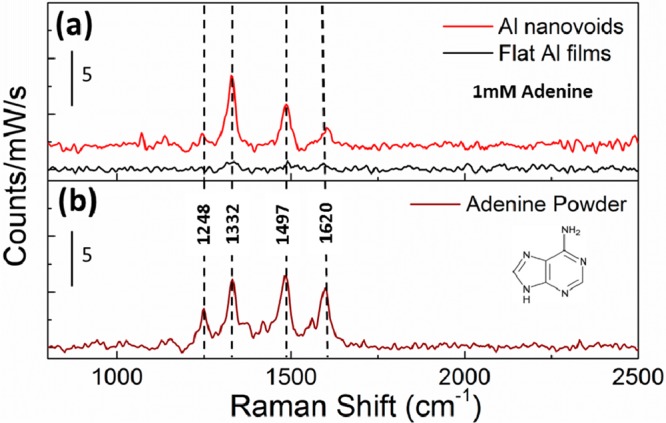
UV Raman spectra of adenine: (a) 1 mM of adenine aqueous solution on Al nanovoids (red line) and flat Al films (black line), (b) bulk adenine powders.
In conclusion, we have developed a large scale Al nanovoid-type substrate for UV-SERS detection based on simple nanofabricaton techniques, combining nanoassembly, ion milling, nanoimprinting and e-beam evaporation. The unique advantage of using nanoimprinting rather than colloidal lithography to generate these nanovoids is the much more facile and scalable fabrication, which produces stamps that can be reused many times and thus are suited for integrating into large-scale rollers in a roll-to-roll process. The well-developed polymer opal system makes the preparation of the colloidal stamps straightforward, enabled by the massive scalability and high quality of the POFs, as well as the intrinsically sticky polymer matrix, which maintains the integrity of the colloidal stamp. The nanovoid geometry is capable of generating concentrated plasmonic fields localized at the edge and interior of the nanovoids, which enhance the Raman signal of adenine more than 3 orders of magnitude compared to planar metal substrates. Such UV-SERS substrates are of great potential interest for the detection of various biomolecules in assays, and flow processes, as well as for environmental sensing and biomedical screening.
Acknowledgments
The authors acknowledge the financial support of PSi for this research.
Supporting Information Available
Experimental details, SEM image of SiO2@PMMA@PEA polymer opal films after oxygen plasma treatment, optical setup for the scattering measurement, surface profile comparison between the stamp and nanovoids, zoomed-in scattering spectra of flat Al films and UV SERS of many different spots. This material is available free of charge via the Internet at http://pubs.acs.org.
Author Contributions
The manuscript was written through contributions of all authors. All authors have given approval to the final version of the manuscript.
We acknowledge financial support from EPSRC grant EP/G060649/1, EP/I012060/1, EP/J007552/1, ERC grant LINASS 320503.
The authors declare no competing financial interest.
Supplementary Material
References
- Fleischmann M.; Hendra P. J.; McQuillan A. J. Raman Spectra of Pyridine Adsorbed at a Silver Electrode. Chem. Phys. Lett. 1974, 26, 163–166. [Google Scholar]
- Jeanmaire D. L.; Van Duyne R. P. Surface Raman Spectroelectrochemistry: Part I. Heterocyclic, Aromatic, and Aliphatic Amines Adsorbed on the Anodized Silver Electrode. J. Electroanal. Chem. Interfacial Electrochem. 1977, 84, 1–20. [Google Scholar]
- Albrecht M. G.; Creighton J. A. Anomalously Intense Raman Spectra of Pyridine at a Silver Electrode. J. Am. Chem. Soc. 1977, 99, 5215–5217. [Google Scholar]
- Grzelczak M.; Liz-Marzan L. M. Colloidal Nanoplasmonics: From Building Blocks to Sensing Devices. Langmuir 2013, 29, 4652–4663. [DOI] [PubMed] [Google Scholar]
- Hugall J. T.; Baumberg J. J.; Mahajan S. Surface-Enhanced Raman Spectroscopy of Cdse Quantum Dots on Nanostructured Plasmonic Surfaces. Appl. Phys. Lett. 2009, 95, 141111. [Google Scholar]
- Savage K. J.; Hawkeye M. M.; Esteban R.; Borisov A. G.; Aizpurua J.; Baumberg J. J. Revealing the Quantum Regime in Tunnelling Plasmonics. Nature 2012, 491, 574–577. [DOI] [PubMed] [Google Scholar]
- Asher S. A. UV Resonance Raman Spectroscopy for Analytical, Physical, and Biophysical Chemistry. Anal. Chem. 1993, 65, 201A–210A. [DOI] [PubMed] [Google Scholar]
- López-Díez E. C.; Goodacre R. Characterization of Microorganisms Using UV Resonance Raman Spectroscopy and Chemometrics. Anal. Chem. 2003, 76, 585–591. [DOI] [PubMed] [Google Scholar]
- Efremov E. V.; Ariese F.; Mank A. J. G.; Gooijer C. Strong Overtones and Combination Bands in Ultraviolet Resonance Raman Spectroscopy. Anal. Chem. 2006, 78, 3152–3157. [DOI] [PubMed] [Google Scholar]
- Ren B.; Lin X.-F.; Yang Z.-L.; Liu G.-K.; Aroca R. F.; Mao B.-W.; Tian Z.-Q. Surface-Enhanced Raman Scattering in the Ultraviolet Spectral Region: UV-SERS on Rhodium and Ruthenium Electrodes. J. Am. Chem. Soc. 2003, 125, 9598–9599. [DOI] [PubMed] [Google Scholar]
- Cui L.; Mahajan S.; Cole R. M.; Soares B.; Bartlett P. N.; Baumberg J. J.; Hayward I. P.; Ren B.; Russell A. E.; Tian Z. Q. Uv Sers at Well Ordered Pd Sphere Segment Void (SSV) Nanostructures. Phys. Chem. Chem. Phys. 2009, 11, 1023–1026. [DOI] [PubMed] [Google Scholar]
- Kämmer E.; Dörfer T.; Csáki A.; Schumacher W.; Da Costa Filho P. A.; Tarcea N.; Fritzsche W.; Rösch P.; Schmitt M.; Popp J. Evaluation of Colloids and Activation Agents for Determination of Melamine Using UV-SERS. J. Phys. Chem. C 2012, 116, 6083–6091. [DOI] [PMC free article] [PubMed] [Google Scholar]
- Cui L.; Wang A.; Wu D.-Y.; Ren B.; Tian Z.-Q. Shaping and Shelling Pt and Pd Nanoparticles for Ultraviolet Laser Excited Surface-Enhanced Raman Scattering. J. Phys. Chem. C 2008, 112, 17618–17624. [Google Scholar]
- Sands H. S.; Demangeot F.; Bonera E.; Webster S.; Bennett R.; Hayward I. P.; Marchi F.; Smith D. A.; Batchelder D. N. Development of a Combined Confocal and Scanning near-Field Raman Microscope for Deep UV Laser Excitation. J. Raman. Spectrosc. 2002, 33, 730–739. [Google Scholar]
- Taguchi A.; Hayazawa N.; Furusawa K.; Ishitobi H.; Kawata S. Deep-UV Tip-Enhanced Raman Scattering. J. Raman. Spectrosc. 2009, 40, 1324–1330. [Google Scholar]
- Sigle D. O.; Perkins E.; Baumberg J. J.; Mahajan S. Reproducible Deep-UV SERS on Aluminum Nanovoids. J. Phys. Chem. Lett. 2013, 4, 1449–1452. [DOI] [PubMed] [Google Scholar]
- Li L.; Fang Lim S.; Puretzky A. A.; Riehn R.; Hallen H. D. Near-Field Enhanced Ultraviolet Resonance Raman Spectroscopy Using Aluminum Bow-Tie Nano-Antenna. Appl. Phys. Lett. 2012, 101, 113116. [DOI] [PMC free article] [PubMed] [Google Scholar]
- Jha S. K.; Ahmed Z.; Agio M.; Ekinci Y.; Löffler J. F. Deep-UV Surface-Enhanced Resonance Raman Scattering of Adenine on Aluminum Nanoparticle Arrays. J. Am. Chem. Soc. 2012, 134, 1966–1969. [DOI] [PubMed] [Google Scholar]
- Dörfer T.; Schmitt M.; Popp J. Deep-UV Surface-Enhanced Raman Scattering. J. Raman. Spectrosc. 2007, 38, 1379–1382. [Google Scholar]
- Mogensen K. B.; Guhlke M.; Kneipp J.; Kadkhodazadeh S.; Wagner J. B.; Espina Palanco M.; Kneipp H.; Kneipp K. Surface-Enhanced Raman Scattering on Aluminum Using near Infrared and Visible Excitation. Chem. Commun. 2014, 50, 3744–3746. [DOI] [PubMed] [Google Scholar]
- Fernando K. A. S.; Smith M. J.; Harruff B. A.; Lewis W. K.; Guliants E. A.; Bunker C. E. Sonochemically Assisted Thermal Decomposition of Alane N,N-Dimethylethylamine with Titanium (IV) Isopropoxide in the Presence of Oleic Acid to Yield Air-Stable and Size-Selective Aluminum Core–Shell Nanoparticles. J. Phys. Chem. C 2008, 113, 500–503. [Google Scholar]
- Li H.; Meziani M. J.; Lu F.; Bunker C. E.; Guliants E. A.; Sun Y.-P. Templated Synthesis of Aluminum Nanoparticles: a New Route to Stable Energetic Materials. J. Phys. Chem. C 2009, 113, 20539–20542. [Google Scholar]
- Stratakis E.; Barberoglou M.; Fotakis C.; Viau G.; Garcia C.; Shafeev G. A. Generation of Al Nanoparticles Via Ablation of Bulk Al in Liquids with Short Laser Pulses. Opt. Express 2009, 17, 12650–12659. [DOI] [PubMed] [Google Scholar]
- Viau G.; Collière V.; Lacroix L. M.; Shafeev G. A. Internal Structure of Al Hollow Nanoparticles Generated by Laser Ablation in Liquid Ethanol. Chem. Phys. Lett. 2011, 501, 419–422. [Google Scholar]
- Maidecchi G.; Gonella G.; Proietti Zaccaria R.; Moroni R.; Anghinolfi L.; Giglia A.; Nannarone S.; Mattera L.; Dai H.-L.; Canepa M.; Bisio F. Deep Ultraviolet Plasmon Resonance in Aluminum Nanoparticle Arrays. ACS Nano 2013, 7, 5834–5841. [DOI] [PubMed] [Google Scholar]
- Baumberg J. J.; Kelf T. A.; Sugawara Y.; Cintra S.; Abdelsalam M. E.; Bartlett P. N.; Russell A. E. Angle-Resolved Surface-Enhanced Raman Scattering on Metallic Nanostructured Plasmonic Crystals. Nano Lett. 2005, 5, 2262–2267. [DOI] [PubMed] [Google Scholar]
- Cole R. M.; Baumberg J. J.; Garcia de Abajo F. J.; Mahajan S.; Abdelsalam M.; Bartlett P. N. Understanding Plasmons in Nanoscale Voids. Nano Lett. 2007, 7, 2094–2100. [Google Scholar]
- Edel J. B.; Kornyshev A. A.; Urbakh M. Self-Assembly of Nanoparticle Arrays for Use as Mirrors, Sensors, and Antennas. ACS Nano 2013, 7, 9526–9532. [DOI] [PubMed] [Google Scholar]
- Wang X. D.; Graugnard E.; King J. S.; Wang Z. L.; Summers C. J. Large-Scale Fabrication of Ordered Nanobowl Arrays. Nano Lett. 2004, 4, 2223–2226. [Google Scholar]
- Chen J.; Chao D.; Lu X.; Zhang W.; Manohar S. K. General Synthesis of Two-Dimensional Patterned Conducting Polymer-Nanobowl Sheet Via Chemical Polymerization. Macromol. Rapid Commun. 2006, 27, 771–775. [Google Scholar]
- Kralchevsky P. A.; Nagayama K. Capillary Interactions between Particles Bound to Interfaces, Liquid Films and Biomembranes. Adv. Colloid Interface Sci. 2000, 85, 145–192. [DOI] [PubMed] [Google Scholar]
- Li Q.; Jonas U.; Zhao X. S.; Kappl M. The Forces at Work in Colloidal Self-Assembly: A Review on Fundamental Interactions between Colloidal Particles. Asia Pac. J. Chem. Eng. 2008, 3, 255–268. [Google Scholar]
- Finlayson C. E.; Spahn P.; Snoswell D. R. E.; Yates G.; Kontogeorgos A.; Haines A. I.; Hellmann G. P.; Baumberg J. J. 3D Bulk Ordering in Macroscopic Solid Opaline Films by Edge-Induced Rotational Shearing. Adv. Mater. 2011, 23, 1540–1544. [DOI] [PubMed] [Google Scholar]
- Plettl A.; Enderle F.; Saitner M.; Manzke A.; Pfahler C.; Wiedemann S.; Ziemann P. Non-Close-Packed Crystals from Self-Assembled Polystyrene Spheres by Isotropic Plasma Etching: Adding Flexibility to Colloid Lithography. Adv. Funct. Mater. 2009, 19, 3279–3284. [Google Scholar]
- Ding T.; Wang F.; Song K.; Yang G.; Tung C.-H. Oxygen Plasma Etching-Induced Crystalline Lattice Transformation of Colloidal Photonic Crystals. J. Am. Chem. Soc. 2010, 132, 17340–17342. [DOI] [PubMed] [Google Scholar]
- Ding T.; Song K.; Yang G.; Tung C.-H. Tunable Fabrication of Two-Dimensional Arrays of Polymer Nanobowls for Biomimic Growth of Amorphous Calcium Carbonate. Macromol. Rapid Commun. 2012, 33, 1562–1567. [DOI] [PubMed] [Google Scholar]
- Howitt D. G. Ion Milling of Materials Science Specimens for Electron Microscopy: A Review. J. Electron. Microsc. Technol. 1984, 1, 405–414. [Google Scholar]
Associated Data
This section collects any data citations, data availability statements, or supplementary materials included in this article.


