Abstract
Comparison of resistive switching memory characteristics using copper (Cu) and aluminum (Al) electrodes on GeOx/W cross-points has been reported under low current compliances (CCs) of 1 nA to 50 μA. The cross-point memory devices are observed by high-resolution transmission electron microscopy (HRTEM). Improved memory characteristics are observed for the Cu/GeOx/W structures as compared to the Al/GeOx/W cross-points owing to AlOx formation at the Al/GeOx interface. The RESET current increases with the increase of the CCs varying from 1 nA to 50 μA for the Cu electrode devices, while the RESET current is high (>1 mA) and independent of CCs varying from 1 nA to 500 μA for the Al electrode devices. An extra formation voltage is needed for the Al/GeOx/W devices, while a low operation voltage of ±2 V is needed for the Cu/GeOx/W cross-point devices. Repeatable bipolar resistive switching characteristics of the Cu/GeOx/W cross-point memory devices are observed with CC varying from 1 nA to 50 μA, and unipolar resistive switching is observed with CC >100 μA. High resistance ratios of 102 to 104 for the bipolar mode (CCs of 1 nA to 50 μA) and approximately 108 for the unipolar mode are obtained for the Cu/GeOx/W cross-points. In addition, repeatable switching cycles and data retention of 103 s are observed under a low current of 1 nA for future low-power, high-density, nonvolatile, nanoscale memory applications.
Keywords: Memory, Resistive switches, GeOx, Copper, Aluminum, Solid electrolyte
Background
Recently, resistive switching memory devices involving different materials such as Pr0.7Ca0.3MnO3 (PCMO) [1], NiOx[2], SrTiO3[3,4], TaOx[5-8], HfOx[9,10], TiO2[11], ZrO2[12], Na0.5Bi0.5TiO3[13], and AlOx[14-16] are widely reported to replace conventional flash memory. On the other hand, conductive bridging resistive random access memory (CBRAM) involving the migration of cations (Ag+ or Cuz+, z = 1, 2) in solid electrolytes such as GexSe1-x[17-20], GeS2[21], Ta2O5[22], ZrO2[23-25], TiOx/ZrO2[26], GeSex/TaOx[27], HfO2[28], CuTe/Al2O3[29], Ti/TaOx[30], ZnO [31], SiO2[32], and GeOx[33] is also reported. In this case, the mobile Ag+ or Cuz+ ions play an important role in the formation and dissolution of metallic filament in the solid electrolytes. Although memory characteristics using different solid electrolytes have been reported, GeOx-based CBRAM devices in the cross-point structure are also a beneficial choice. Memory characteristics using GeOx film in a Cu/GeOx/Al structure were first reported by Beynon and El-Samanoudy in 1987 [34]. Their extended work was published in 1991 using a Cu/GeOx/Au structure [35]. Resistive switching memory using GeOx material in different structures such as Ni/GeOx/SrTiOx/TaN [36] and Pt/SiGeOx/SiGeON/TiN [37] has also been reported for future nonvolatile memory applications. On one hand, Schindler et al. [38] has reported a GeOx layer for the Cu (Ag) diffusion barrier layer in a Cu (Ag)/GeSe/Pt structure. On the other hand, cross-point structures using different switching materials have been reported by several groups [6,39-42] to have a high-density memory for future applications. It is known that resistive switching memories in cross-point architecture possess several attractive features and have attracted considerable attention in recent years because of the multilayer stacking of three-dimensional (3D) architecture, simplicity of their manufacturing, and the simplest interconnection configuration. Furthermore, resistive switching memory devices with low-current operation (<100 μA) are also an important issue. To mitigate those specifications, a cross-point memory using a Cu/GeOx/W structure has been compared with that using an Al/GeOx/W structure for the first time.
In this study, the memory characteristics using Cu and Al top electrodes (TEs) on GeOx/W cross-points have been compared. The cross-point structures were observed by high-resolution transmission electron microscopy (HRTEM). The Cu/GeOx/W cross-point memory devices have shown improved bipolar resistive switching characteristics as compared to the Al/GeOx/W cross-points, owing to the AlOx layer formation at the Al/GeOx interface. The RESET current deceases with the decrease of current compliances (CCs) from 50 μA to 1 nA for the Cu/GeOx/W devices, while the RESET current was independent (>1 mA) of CC in the range of 500 μA to 1 nA for the Al/GeOx/W cross-point memories. High resistance ratios of 102 to 104 under bipolar and approximately 108 under unipolar modes are observed for the Cu/GeOx/W cross-point memory devices. Repeatable switching cycles and data retention of approximately 103 s under a low CC of 1 nA were obtained for the Cu TE devices, which are very useful for low-power operation of high-density nonvolatile nanoscale memory applications.
Methods
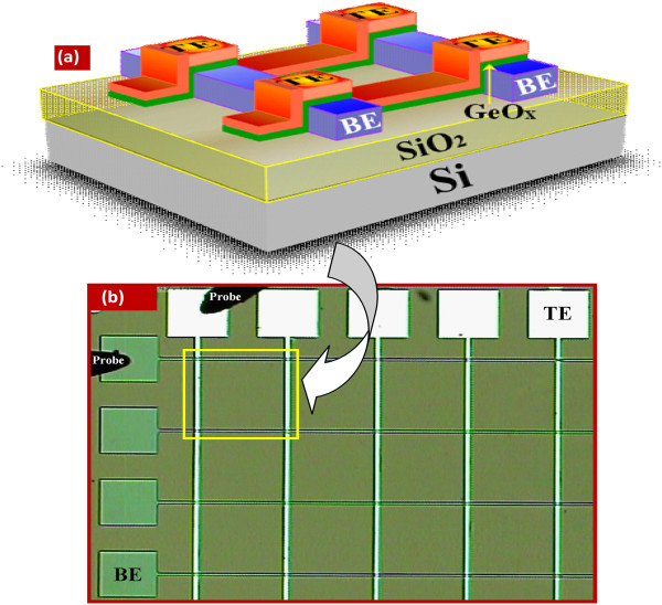
A silicon dioxide (SiO2) layer with a thickness of approximately 200 nm was grown by wet oxidation process on 4-in.p-Si wafers after the Radio Corporation of America (RCA) cleaning method. The horizontal furnace consisted of a quartz tube on a carrier made of quartz glass in the middle; the wafers were placed in the quartz tube. The temperature of the furnace was maintained at 900°C during the oxidation process. To avoid cracks or warping, the wafers were placed inside the furnace at 600°C. The furnace was heated slowly with a ramp rate of +13°C/min. During the oxidation process, hydrogen and oxygen gases were used with flow rates of 4 and 2.5 standard liters per minute (SLM), respectively. The oxidation time was 90 min. Then, W metal as a bottom electrode (BE) with a thickness of approximately 200 nm was deposited by radio frequency (RF) sputtering on SiO2/Si wafers. The deposition parameters of the W layer were shown in Table 1. Then, the BE was defined and patterned by standard photolithography and wet chemical etching processes. The following parameters were used for the photolithography process. The wafer is initially heated at 120°C for 10 min in the oven to drive off any moisture that may be present on the wafer surface. A liquid ‘adhesion promoter’ such as hexamethyldisilazane or HMDS was applied to promote adhesion of the photoresist to the wafer. A spin coater was used to coat the HMDS on the wafer. The spin coating was run at initially 3,000 rpm for 10 s and then 5,000 rpm for 20 s. Following the same process, an AZ6112 positive photoresist (AZ Electronic Materials, Branchburg, NJ, USA) was spun on the wafer to create the pattern. The photoresist-coated wafer was then prebaked to drive off excess photoresist solvent at 90°C for 2 min. After prebaking, the sample was placed on a vacuum substrate of an optical lithography system (ABM Sales Service, San Jose, CA, USA). Then, mask 1 was placed over the sample. The photoresist was exposed to ultraviolet (UV) light for 4 s. Before developing, a postexposure bake (PEB) was performed at 90°C for 1 min to reduce the standing wave phenomena caused by the destructive and constructive interference patterns of the incident light. The wafer was immersed into the AZ330 developer (AZ Electronic Materials) for 15 s to remove the exposed photoresist and then rinsed by deionized (DI) water. The resulting wafer was then ‘hard-baked’ to harden the final resist at 120°C for 15 min. The wet chemical etching process was used to etch the uncovered W metal layer and form the W BE. A commercially available tungsten etchant (Sigma-Aldrich) was used, and the wafer was dipped into the solution for 2 to 3 min. The same photolithography process was repeated to design the 1 × 1 to 10 × 10 arrays. To pattern the switching material and TE, mask 2 was placed over the samples using a mask aligner. After the masking process, the GeOx switching material with a thickness of approximately 10 nm was deposited by the same RF sputtering system. Following this, Cu as a TE with a thickness of approximately 40 nm was deposited using a thermal evaporator. Then, the aluminum (Al) layer with a thickness of approximately 160 nm was deposited in situ by the thermal evaporator. The deposition conditions of GeOx, Cu, and Al were shown in Table 1. Finally, a lift-off process was performed to get the final Al/Cu/GeOx/W (device S1) memory device, i.e., called Cu/GeOx/W structure hereafter. Similarly, an Al/GeOx/W (device S2) memory device without a Cu layer was also prepared for comparison. Table 2 shows the structures of the fabricated memory devices. A schematic illustration of the fabricated GeOx-based cross-point memory device is shown in Figure 1a. The GeOx solid electrolyte is sandwiched between Cu or Al TE and W BE. An optical micrograph (OM) of 4 × 5 cross-points is shown clearly in Figure 1b. All cross-points are clearly observed.
Table 1.
Deposition parameters of different materials
| Materials | Target/granules | Methods | Vacuum (Torr) | Ar gas (SCCM) | Power (Watt) | Deposition rate |
|---|---|---|---|---|---|---|
| W |
W target |
RF sputtering |
1 × 10⁻⁵ |
25 |
150 |
12 nm/min |
| GeOx |
Ge target |
RF sputtering |
2 × 10⁻⁵ |
25 |
50 |
5.3 nm/min |
| Cu |
Cu granules |
Thermal evaporator |
8 × 10⁻⁶ |
- |
- |
2-3 Å/s |
| Al | Al granules | Thermal evaporator | 8 × 10⁻⁶ | - | - | 2-3 Å/s |
Table 2.
Structures of the cross-point resistive switching memory devices
|
Devices |
BE ~ 200 nm |
Switching layer (10 nm) |
TE |
|
|---|---|---|---|---|
| Cu ~ 40 nm | Al ~ 160 nm | |||
| S1 |
W |
GeOx |
√ |
√ |
| S2 | W | GeOx | × | √ |
Figure 1.
Schematic illustration and optical image of the Cu/GeOx/W cross-point memories. (a) Schematic illustration and (b) optical image of our fabricated cross-point memory devices. Active area of the cross-point memory is approximately 1 × 1 μm2. The thickness of the GeOx solid electrolyte film is approximately 10 nm.
The cross-point structure and thicknesses of all materials were evaluated from a HRTEM image. HRTEM was carried out using a FEI Tecnai (Hillsboro, OR, USA) G2 F-20 field emission system. Memory characteristics were measured using an HP4156C semiconductor parameter analyzer (Agilent Technologies, Santa Clara, CA, USA). For electrical measurements, the bias was applied to the TE while the W BE was grounded.
Results and discussion
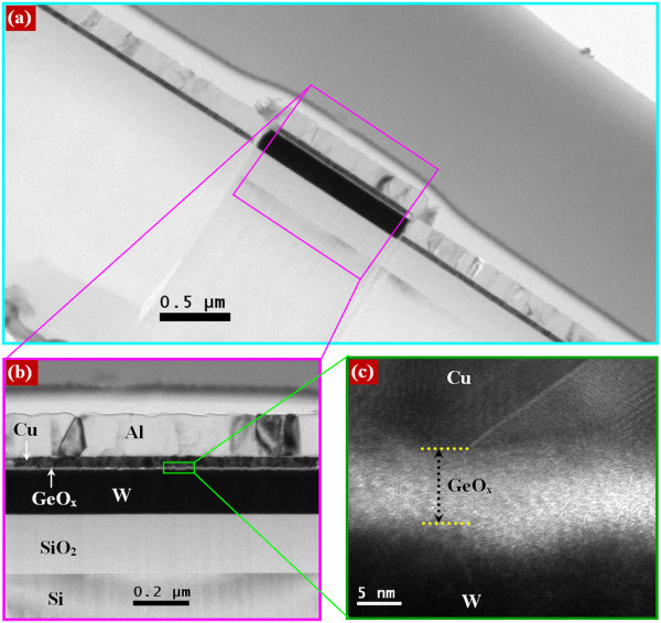
Figure 2 shows the TEM image of the Cu/GeOx/W structure (device S1). The area of the cross-point is approximately 1.2 × 1.2 μm2 (Figure 2a). Films deposited layer by layer are clearly observed in the HRTEM image, as shown in Figure 2b. The thickness of the SiO2 layer is approximately 200 nm. The thicknesses of W, Cu, and Al metals are approximately 180, 38, and 160 nm, respectively. The thickness of the GeOx solid electrolyte is approximately 8 nm, as shown in Figure 2c. The formation of a thin (2 to 3 nm) WOx layer is observed at the GeOx/W interface. The HRTEM image of the Al/GeOx/W cross-point memory devices is also shown in Figure 3a. It is interesting to note that the AlOx layer with a thickness of approximately 5 nm at the Al/GeOx interface is observed (Figure 3b). The Gibbs free energies of the Al2O3, GeO2, CuO, and Cu2O films are -1,582, -518.8, -129.7, and -149 kJ/mol at 300 K, respectively [43]. Therefore, the formation of AlOx at the Al/GeOx interface will be the easiest as compared to those of other materials. For example, the AlOx layer at the Al/Ta2O5 interface was also observed even though the Al layer was deposited on a Ta2O5 film (not shown here). This suggests that Al is a metal reactive with oxygen, and it is hard to control the reaction at the Al/oxide interface. However, the AlOx film will have more defects, which may have resistive switching phenomena. The resistive switching memory characteristics using Cu and Al top electrodes on GeOx/W cross-point memories are discussed below.
Figure 2.
TEM images of the cross-point memories using Cu electrode. (a) TEM image of a Cu/GeOx/W cross-point memory. HRTEM image with scale bars of (b) 0.2 μm and (c) 5 nm. Films deposited layer by layer are clearly observed by HRTEM imaging.
Figure 3.
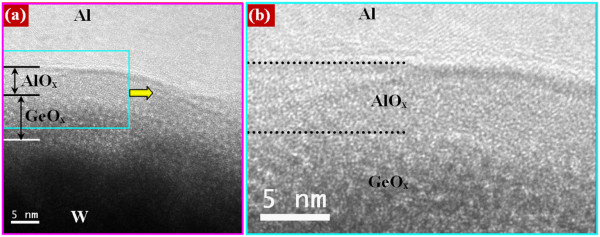
TEM images of the device using Al electrode. (a) HRTEM image of an Al/GeOx/W cross-point memory. (b) Formation of an AlOx film with a thickness of approximately 5 nm at the Al/GeOx interface is observed.
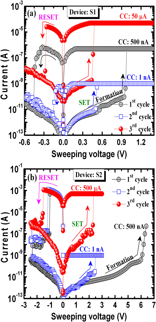
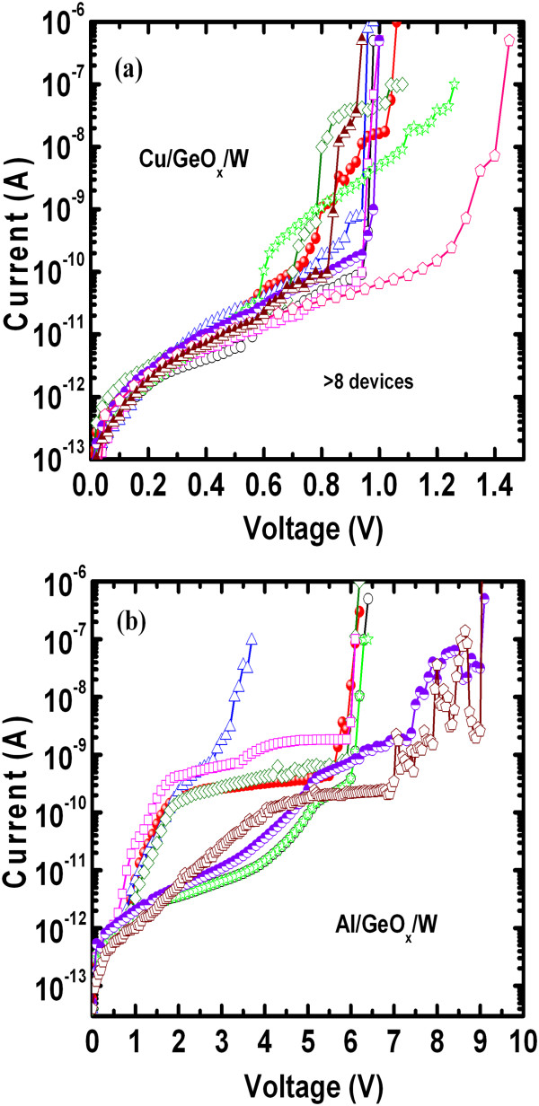
Typical I-V hysteresis with CCs of 1 nA to 50 μA when using the Cu/GeOx/W cross-point memory is shown in Figure 4a. Initially, all memory devices were in high-resistance state (HRS), and positive sweeping voltage was applied. A slightly high voltage of approximately 1 V is necessary to switch the memory device from HRS to low-resistance state (LRS) under a CC of 500 nA, which is shown in the first cycle. This will form a Cu filament in the GeOx solid electrolyte. After the formation process, the device shows normal bipolar resistive switching behavior. The memory device can be operated at a low CC of 1 nA, and a Cu cylindrical-type filament can be expected to form because the currents at HRS are the same after RESET operation for CCs of 1 to 500 nA [33]. A current change at HRS (approximately 1 pA to 1 nA at 0.1 V) is observed at a CC of 50 μA. At a higher CC of 50 μA, the filament diameter increased and the shape of the filament will be conical type [27]. This implies that the Cu filament remains at the GeOx/W interface after RESET operation. On the other hand, a high formation voltage of approximately 6 V is needed for the Al TE, as shown in the first cycle (Figure 4b). In this case, the memory device can be operated at a low CC of 1 nA, but a high RESET current of >1 mA is needed to rupture the conducting filaments. A current change at HRS is observed at a high CC of 500 μA owing to the remaining filament even with a higher RESET current of >1 mA. I-V measurements for pristine devices S1 and S2 are shown in Figure 5a,b. The average leakage currents at 0.1 V of the S2 devices are higher than those of the S1 devices (4.4 pA versus 0.4 pA) owing to the formation of the approximately 5-nm-thick AlOx layer at the Al/GeOx interface. The formation voltages for the S1 devices are 0.8 to 1.4 V, while they are 3 to 9 V for the S2 devices, which is due to the thicker switching material for the Al TE than the Cu TE (8 + 5 = 13 nm versus 8 nm). This is also beneficial to the Cu TE (device S1) than the Al TE (device S2).
Figure 4.
Bipolar resistive switching characteristics. (a) Typical I-V characteristics of Cu/GeOx/W and (b) Al/GeOx/W cross-point memories.
Figure 5.
Current–voltage characteristics.I-V measurements of pristine (a) Cu/GeOx/W (S1) and (b) Al/GeOx/W (S2) devices. A high formation voltage is needed for Al TE. More than eight devices were measured randomly.
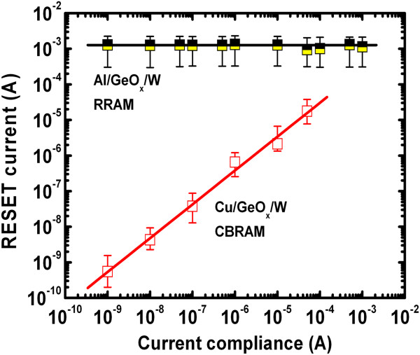
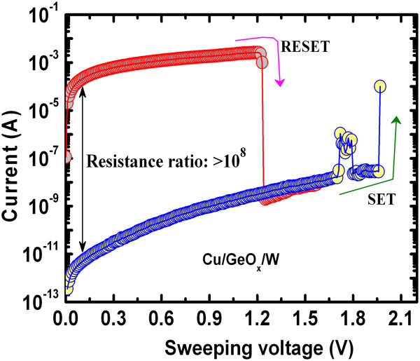
Further, the RESET current is independent of CCs from 1 nA to 1 mA for the Al/GeOx/W cross-point memory device, as shown in Figure 6. This suggests that the RESET current scalability as well as device scaling is difficult for the Al TE devices, which form larger filament diameter (or many conducting filaments) even at a small CC of 1 nA. This is due to a strong current overshoot effect in the Al/GeOx/W cross-point memory devices. It is noted that the diameters of the conducting filaments are the same at all CCs from 1 nA to 2 mA, which is due to the defective AlOx layer at the Al/GeOx interface or unstable interface. A high RESET current of >20 mA was also reported by Kato et al. using Al TE [44]. Lin et al. [12] also reported a high RESET current for Al2O3-based resistive switching memory using a Ti/Al2O3/Pt structure. According to several reported results, using Al electrode or Al2O3-based resistive memory devices requires higher operation voltages as well as high RESET currents [12,44,45]; however, a few results were reported on low-current operation [6-8,14]. As we can see, the formation voltage of the Al/GeOx/W device is higher than that of the Cu/GeOx/W device. It seems that the parasitic capacitance [46] of the Al/GeOx/W device as well as the current overshoot effect is higher. Even if the SET voltage is lower, the RESET current is still very high or the same with the RESET current of formation. This suggests that the current overshoot effect is not due to the higher operation voltage but to the AlOx formation at the Al/GeOx interface or unstable interface. This is a very important difference between these Al and Cu TEs. An excellent scaling of the RESET current is observed for the Cu/GeOx/W cross-point memory devices with CCs from 1 nA to 50 μA. Furthermore, the RESET current is lower than the SET current, which proves no current overshoot effect even in the 1R configuration or no parasitic effect [46]. The formation and dissolution of Cu nanofilament under SET and RESET are responsible for the switching mechanism of the Cu/GeOx/W cross-point memory devices. The Cu ions will migrate through the defects into the GeOx film and start to grow first at the GeOx/W BE under SET operation by reduction process (Cuz+ + ze- → Cuo). The Cu nanofilament will start to dissolve at the Cu/GeOx interface under RESET operation by oxidation process (Cuo → Cuz+ + ze-). In the case of the Al/GeOx/W cross-point memory, oxygen vacancy filament formation and oxidation are responsible for the switching mechanism. When the applied bias voltage is higher than the SET voltage on the Al TE, the Ge-O bonds will break and O2- ions as negative charge will migrate from the GeOx layer towards the Al/GeOx interface, resulting in an oxygen vacancy conducting filament formation. The RESET will occur when the applied negative bias on the Al TE is lower than the RESET voltage and the O2- ions will migrate from the Al/AlOx interface and oxidize the conducting filament. Due to the defective AlOx layer formation at the Al/GeOx interface and Joule heating, uncontrolled oxygen vacancy filament formation and oxidation by O2- ion migration can be assumed under SET and RESET operations, which make reduction of the RESET current as well as scaling of the device difficult. This suggests that the Cu nanofilament diameter can be controlled by external CCs for the Cu/GeOx/W cross-point memories. In addition, unipolar resistive switching characteristics are also observed, as shown in Figure 7. In this case, the Cu filament is formed under SET and the filament is dissolved by Joule heating under RESET. A high resistance ratio of 108was obtained from unipolar switching. Guan et al. [47] have also reported a high resistance ratio of approximately 106using a Cu/ZrO2:Cu/Pt structure. This suggests that our new Cu/GeOx/W cross-point memory is useful for future multilevel cell (MLC) applications.
Figure 6.
Unipolar resistive switching characteristics. Unipolar resistive switching characteristics of the Cu/GeOx/W cross-point memory device. A high resistance ratio of >108 was also obtained using the cross-point architecture.
Figure 7.
RESET current scalability comparison with Cu and Al electrodes. RESET currents versus CCs curve. The RESET current increases as the CCs for Cu TE increase; however, the RESET current is not scalable for Al TE because of the AlOx formation at the Al/GeOx interface.
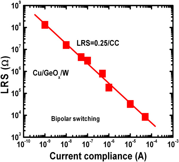
Figure 8 shows the dependence of LRS on CCs ranging from 1 nA to 50 μA for the Cu/GeOx/W cross-point memories. The LRSs decreased linearly with increase of the CCs from 1 nA to 50 μA, which is applicable for MLC operation. By changing CCs (1 nA to few microamperes), more than four orders of magnitude of the LRS is shifted over the same range. If we consider that 3 resistance states per decade can be distinguished [3], the resistive memory using the Cu/GeOx/W structure will allow at least 12 states for the storage. The relationship between LRS and CC is related to the following equation:
| (1) |
Figure 8.
LRS depends on CCs. LRS versus CCs for the Cu/GeOx/W cross-point memory. LRS decreases with increasing CCs. The device can be operated with current as low as 1 nA.
From Equation 1, the average LRS is 0.251/CC, which is close to the reported value of 0.250/CC for metallic filament [33,48]. Therefore, the CBRAM device can be designed easily for low-power MLC operation.
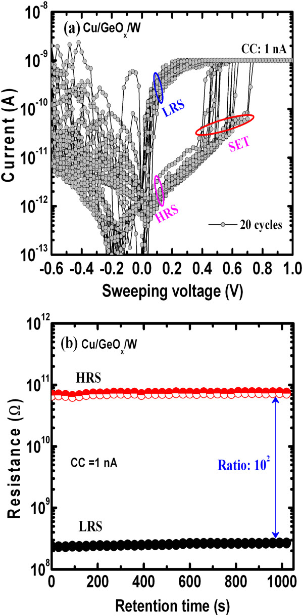
Figure 9a shows repeatable 20 DC switching cycles at a low CC of 1 nA. The SET voltages are varied from 0.4 to 0.8 V, and the RESET current increased after few cycles, which confirms a filament formation after few cycles [20,30]. The data retention of approximately 103 s is also observed under a low operation current of 1 nA (Figure 9b). The resistance ratio is approximately 102. Further study is needed to improve the cross-point resistive switching memory characteristics under low-current operation. In addition, the read pulse endurances of LRS and HRS are more than 105 cycles with a large resistance ratio of >104, and both resistance states are very stable without significant resistance variation for a retention test of more than 104 s under a CC of 50 μA (not shown here), which can be applicable for future low-power high-density nonvolatile memory applications.
Figure 9.
Switching cycles and data retention. (a) Repeatable switching cycles and (b) data retention of the Cu/GeOx/W cross-point memory devices under a low CC of 1 nA.
Conclusions
Resistive switching memory characteristics using Cu and Al TEs on the GeOx/W cross-point memory devices have been compared. Improved memory characteristics of the Cu/GeOx/W structures under low current varying from 1 nA to 50 μA and a low voltage operation of ±2 V are observed as compared to those of the Al/GeOx/W structures. These cross-point memory structures are observed by HRTEM. The formation of AlOx layer with a thickness of approximately 5 nm at the Al/GeOx interface is observed, which is unstable to control the resistive switching phenomena. The RESET current scalability is observed for Cu TE, while it is high (>1 mA) and independent for the Al TE with CCs varying from 1 nA to 500 μA. Superior resistive switching memory performances in terms of high resistance ratio (102 to 104 under bipolar and approximately 108 under unipolar modes), long pulse endurance of >105 cycles under a CC of 50 μA, and good scalability potential are observed for the Cu/GeOx/W cross-point memory devices. Repeatable switching cycles and data retention of 103 s are also observed under a low CC of 1 nA. This study is important for high-density low-power 3D architecture in the future.
Competing interests
The authors declare that they have no competing interests.
Authors’ contributions
SZR fabricated and measured the cross-point memory devices under the instruction of SM. SM arranged and finalized the manuscript. Both authors contributed to the preparation and revision of the manuscript and approved it for publication.
Contributor Information
Sheikh Ziaur Rahaman, Email: d9628301@stmail.cgu.edu.tw.
Siddheswar Maikap, Email: sidhu@mail.cgu.edu.tw.
Acknowledgements
This work was supported by the National Science Council (NSC), Taiwan, under contract numbers NSC-101-2221-E-182-061 and NSC-102-2221-E-182-057-MY2.
References
- Sawa A. Resistive switching in transition metal oxides. Mater Today. 2008;11:28. [Google Scholar]
- Kim DC, Seo S, Ahn SE, Suh DS, Lee MJ, Park BH, Yoo IK, Baek IG, Kim HJ, Yim EK, Lee JE, Park SO, Kim HS, Chung UI, Moon JT, Ryu BI. Electrical observations of filamentary conductions for the resistive memory switching in NiO films. Appl Phys Lett. 2006;88:202102. doi: 10.1063/1.2204649. [DOI] [Google Scholar]
- Waser R, Aono M. Nanoionics-based resistive switching memories. Nat Mater. 2007;6:833. doi: 10.1038/nmat2023. [DOI] [PubMed] [Google Scholar]
- Sun X, Li G, Chen L, Shi Z, Zhang W. Bipolar resistance switching characteristics with opposite polarity of Au/SrTiO3/Ti memory cells. Nanoscale Res Lett. 2011;6:599. doi: 10.1186/1556-276X-6-599. [DOI] [PMC free article] [PubMed] [Google Scholar]
- Ninomiya T, Wei Z, Muraoka S, Yasuhara R, Katayama K, Takagi T. Conductive filament scaling of TaOx bipolar ReRAM for improving data retention under low operation current. IEEE Trans Electron Devices. 2013;60:1384. [Google Scholar]
- Lee MJ, Lee CB, Lee D, Lee SR, Chang M, Hur JH, Kim YB, Kim CJ, Seo DH, Seo S. A fast, high-endurance and scalable non-volatile memory device made from asymmetric Ta2O5-x/TaO2-x bilayer structures. Nat Mater. 2011;10:625. doi: 10.1038/nmat3070. [DOI] [PubMed] [Google Scholar]
- Prakash A, Maikap S, Chiu H-C, Tien T-C, Lai C-S. Enhanced resistive switching memory characteristics and mechanism using a Ti nanolayer at the W/TaOx interface. Nanoscale Res Lett. 2013;8:288. doi: 10.1186/1556-276X-8-288. [DOI] [PMC free article] [PubMed] [Google Scholar]
- Prakash A, Jana D, Maikap S. TaOx-based resistive switching memories: prospective and challenges. Nanoscale Res Lett. 2013;8:418. doi: 10.1186/1556-276X-8-418. [DOI] [PMC free article] [PubMed] [Google Scholar]
- Chen YS, Lee HY, Chen PS, Wu TY, Wang CC, Tzeng PJ, Chen F, Tsai MJ, Lien C. An ultrathin forming-free HfOx resistance memory with excellent electrical performance. IEEE Electron Device Lett. 2010;31:1473. [Google Scholar]
- Chen YY, Goux L, Clima S, Govoreanu B, Degraeve R, Kar GS, Fantini A, Groeseneken G, Wouters DJ, Jurczak M. Endurance/retention trade-off on HfO2/metal cap 1T1R bipolar RRAM. IEEE Trans Electron Devices. 2013;60:1114. [Google Scholar]
- Kwon DH, Kim KM, Jang JH, Jeon JM, Lee MH, Kim GH, Li XS, Park GS, Lee B, Han S, Kim M, Hwang CS. Atomic structure of conducting nanofilaments in TiO2 resistive switching memory. Nat Nanotechnol. 2010;5:148. doi: 10.1038/nnano.2009.456. [DOI] [PubMed] [Google Scholar]
- Lin CY, Wu CY, Wu CY, Lee TC, Yang FL, Hu C, Tseng TY. Effect of top electrode material on resistive switching properties of ZrO2film memory devices. IEEE Electron Device Lett. 2007;28:366. [Google Scholar]
- Zhang T, Zhang X, Ding L, Zhang W. Study on resistance switching properties of Na0.5Bi0.5TiO3thin films using impedance spectroscopy. Nanoscale Res Lett. 2009;4:1309. doi: 10.1007/s11671-009-9397-4. [DOI] [PMC free article] [PubMed] [Google Scholar]
- Wu Y, Lee B, Wong HSP. Al2O3-based RRAM using atomic layer deposition (ALD) with 1-μA RESET current. IEEE Electron Device Lett. 2010;31:1449. [Google Scholar]
- Banerjee W, Maikap S, Lai CS, Chen YY, Tien TC, Lee HY, Chen WS, Chen FT, Kao MJ, Tsai MJ, Yang JR. Formation polarity dependent improved resistive switching memory characteristics using nanoscale (1.3 nm) core-shell IrOx nano-dots. Nanoscale Res Lett. 2012;7:194. doi: 10.1186/1556-276X-7-194. [DOI] [PMC free article] [PubMed] [Google Scholar]
- Prakash A, Maikap S, Banerjee W, Jana D, Lai CS. Impact of electrically formed interfacial layer and improved memory characteristics of IrOx/high-κx/W structures containing AlOx, GdOx, HfOx, and TaOx switching materials. Nanoscale Res Lett. 2013;8:379. doi: 10.1186/1556-276X-8-379. [DOI] [PMC free article] [PubMed] [Google Scholar]
- Kund M, Beitel G, Pinnow CU, Röhr T, Schumann J, Symanczyk R, Ufert KD, Müller G. IEEE International Electron Devices Meeting. IEDM Technical Digest: 5–7 December 2005. Washington, DC: Piscataway: IEEE; 2005. Conductive bridging RAM (CBRAM): an emerging non-volatile memory technology scalable to sub 20 nm; pp. 754–757. [Google Scholar]
- Rahaman SZ, Maikap S, Chiu HC, Lin CH, Wu TY, Chen YS, Tzeng PJ, Chen F, Kao MJ, Tsai MJ. Bipolar resistive switching memory using Cu metallic filament in Ge0.4Se0.6solid-electrolyte. Electrochem Solid-State Lett. 2010;13:H159. doi: 10.1149/1.3339449. [DOI] [Google Scholar]
- Yu S, Wong HSP. Compact modeling of conducting-bridge random-access memory (CBRAM) IEEE Trans Electron Dev. 2011;58:1352. [Google Scholar]
- Rahaman SZ, Maikap S, Das A, Prakash A, Wu YH, Lai CS, Tien TC, Chen WS, Lee HY, Chen FT, Tsai MJ, Chang LB. Enhanced nanoscale resistive memory characteristics and switching mechanism using high Ge content Ge0.5Se0.5 solid electrolyte. Nanoscale Res Lett. 2012;7:614. doi: 10.1186/1556-276X-7-614. [DOI] [PMC free article] [PubMed] [Google Scholar]
- Jameson JR, Gilbert N, Koushan F, Saenz J, Wang J, Hollmer S, Kozicki MN. One-dimensional model of the programming kinetics of conductive-bridge memory cells. Appl Phys Lett. 2011;99:063506. doi: 10.1063/1.3623485. [DOI] [Google Scholar]
- Sakamoto T, Lister K, Banno N, Hasegawa T, Terabe K, Aono M. Electronic transport in Ta2O5 resistive switch. Appl Phys Lett. 2007;91:092110. doi: 10.1063/1.2777170. [DOI] [Google Scholar]
- Liu Q, Long S, Lv H, Wang W, Niu J, Huo Z, Chen J, Liu M. Controllable growth of nanoscale conductive filaments in solid-electrolyte-based ReRAM by using a metal nanocrystal covered bottom electrode. ACS Nano. 2010;4:6162. doi: 10.1021/nn1017582. [DOI] [PubMed] [Google Scholar]
- Liu Q, Sun J, Lv H, Long S, Yin K, Wan N, Li Y, Sun L, Liu M. Real-time observation on dynamic growth/dissolution of conductive filaments in oxide-electrolyte-based ReRAM. Adv Mater. 1844;2012:24. doi: 10.1002/adma.201104104. [DOI] [PubMed] [Google Scholar]
- Liu Q, Long S, Wang W, Tanachutiwat S, Li Y, Wang Q, Zhang M, Huo Z, Chen J, Liu M. Low-power and highly uniform switching in ZrO2-based ReRAM with a Cu nanocrystal insertion layer. IEEE Electron Device Letters. 2010;31:1299. [Google Scholar]
- Li Y, Long S, Lv H, Liu Q, Wang Y, Zhang S, Lian W, Wang M, Zhang K, Xie H, Liu S, Liu M. Improvement of resistive switching characteristics in ZrO2film by embedding a thin TiOx layer. Nanotechnology. 2011;22:254028. doi: 10.1088/0957-4484/22/25/254028. [DOI] [PubMed] [Google Scholar]
- Rahaman SZ, Maikap S, Chen WS, Lee HY, Chen FT, Tien TC, Tsai MJ. Impact of TaOx nanolayer at the GeSex/W interface on resistive switching memory performance and investigation of Cu nanofilament. J Appl Phys. 2012;111:063710. doi: 10.1063/1.3696972. [DOI] [Google Scholar]
- Nagata T, Haemori M, Yamashita Y, Yoshikawa H, Iwashita Y, Kobayashi K, Chikyow T. Bias application hard x-ray photoelectron spectroscopy study of forming process of Cu/HfO2/Pt resistive random access memory structure. Appl Phys Lett. 2011;99:223517. doi: 10.1063/1.3664781. [DOI] [Google Scholar]
- Goux L, Opsomer K, Degraeve R, Muller R, Detavernier C, Wouters DJ, Jurczak M, Altimime L, Kittl JA. Influence of the Cu-Te composition and microstructure on the resistive switching of Cu-Te/Al2O3/Si cells. Appl Phys Lett. 2011;99:053502. doi: 10.1063/1.3621835. [DOI] [Google Scholar]
- Rahaman SZ, Maikap S, Tien TC, Lee HY, Chen WS, Chen F, Kao MJ, Tsai MJ. Excellent resistive memory characteristics and switching mechanism using a Ti nanolayer at the Cu/TaOx interface. Nanoscale Res Lett. 2012;7:345. doi: 10.1186/1556-276X-7-345. [DOI] [PMC free article] [PubMed] [Google Scholar]
- Peng S, Zhuge F, Chen X, Zhu X, Hu B, Pan L, Chen B, Li RW. Mechanism for resistive switching in an oxide-based electrochemical metallization memory. Appl Phys Lett. 2012;100:072101. doi: 10.1063/1.3683523. [DOI] [Google Scholar]
- Yang Y, Gao P, Gaba S, Chang T, Pan X, Lu W. Observation of conducting filament growth in nanoscale resistive memories. Nat Commun. 2012;3:1737. doi: 10.1038/ncomms1737. [DOI] [PubMed] [Google Scholar]
- Rahaman SZ, Maikap S, Chen WS, Lee HY, Chen FT, Kao MJ, Tsai MJ. Repeatable unipolar/bipolar resistive memory characteristics and switching mechanism using a Cu nanofilament in a GeOx film. Appl Phys Lett. 2012;101:073106. doi: 10.1063/1.4745783. [DOI] [PMC free article] [PubMed] [Google Scholar]
- Beynon J, El-Samanoudy MM. Memory phenomena in reactively-evaporated AlOx and GeOx thin films. J Mater Sci Lett. 1987;6:1447. doi: 10.1007/BF01689318. [DOI] [Google Scholar]
- El-Samanoudy MM, Beynon J. Scanning electron microscopy and electron microprobe analysis of Au-GeOx-Cu and Au-AlOx-Cu sandwich structures. J Mater Sci. 1991;26:2431. doi: 10.1007/BF01130191. [DOI] [Google Scholar]
- Cheng C, Chin A, Yeh F. Stacked GeO/SrTiOx resistive memory with ultralow resistance currents. Appl Phys Lett. 2011;98:052905. doi: 10.1063/1.3549689. [DOI] [Google Scholar]
- Syu YE, Chang TC, Tsai CT, Chang GW, Tsai TM, Chang KC, Tai YH, Tsai MJ, Sze SM. Improving resistance switching characteristics with SiGeOx/SiGeON double layer for nonvolatile memory applications. Electrochem Solid State Lett. 2011;14:H419. doi: 10.1149/1.3615823. [DOI] [Google Scholar]
- Schindler C, Guo X, Besmehn A, Waser R. Resistive switching in Ge0.3Se0.7 films by means of copper ion migration. Z Phys Chem. 2007;221:1469. doi: 10.1524/zpch.2007.221.11-12.1469. [DOI] [Google Scholar]
- Yang JJ, Pickett MD, Li X, Ohlberg DAA, Stewart DR, Williams RS. Memristive switching mechanism for metal/oxide/metal nanodevices. Nat Nanotechnol. 2008;3:429. doi: 10.1038/nnano.2008.160. [DOI] [PubMed] [Google Scholar]
- Kügeler C, Meier M, Rosezin R, Gilles S, Waser R. High density 3D memory architecture based on the resistive switching effect. Solid-State Electron. 2009;53:1287. doi: 10.1016/j.sse.2009.09.034. [DOI] [Google Scholar]
- Borghetti J, Snider GS, Kuekes PJ, Yang JJ, Stewart DR, Williams RS. Memristive switches enable stateful logic operations via material implication. Nature. 2010;464:873. doi: 10.1038/nature08940. [DOI] [PubMed] [Google Scholar]
- Xia Q, Yang JJ, Wu W, Li X, Williams RS. Self-aligned memristor cross-point arrays fabricated with one nanoimprint lithography step. Nano Lett. 2010;10:2909. doi: 10.1021/nl1017157. [DOI] [PubMed] [Google Scholar]
- Birks N, Meier GH, Pettit FS. Introduction to the High Temperature Oxidation of Metals. Cambridge: Cambridge University Press; 2006. [Google Scholar]
- Kato S, Nigo S, Lee JW, Mihalik M, Kitazawa H, Kido G. Transport properties of anodic porous alumina for ReRAM. J Phys Conf Ser. 2008;109:012017. [Google Scholar]
- Song J, Inamdar AI, Jang BU, Jeon K, Kim YS, Jung K, Kim Y, Im H, Jung W, Kim H. Effects of ultrathin Al layer insertion on resistive switching performance in an amorphous aluminum oxide resistive memory. Appl Phys Express. 2010;3:091101. doi: 10.1143/APEX.3.091101. [DOI] [Google Scholar]
- Kinoshita K, Tsunoda K, Sato Y, Noshiro H, Yagaki S, Aoki M, Sugiyama Y. Reduction in the reset current in a resistive random access memory consisting of NiOx brought about by reducing a parasitic capacitance. Appl Phy Lett. 2008;93:033506. doi: 10.1063/1.2959065. [DOI] [Google Scholar]
- Guan W, Long S, Liu Q, Liu M, Wang W. Nonpolar nonvolatile resistive switching in Cu doped ZrO2. IEEE Electron Device Letters. 2008;29:434. [Google Scholar]
- Kozicki MN, Mitkova M. In: Nanotechnology. Waser R, editor. Weinheim: Wiley; 2008. Memory devices based on mass transport in solid electrolytes. 3. [Google Scholar]


