Abstract
Graphene has attracted considerable interest as a potential material for future electronics. Although mechanical peel is known to produce high quality graphene flakes, practical applications require continuous graphene layers over a large area. The catalyst-assisted chemical vapor deposition (CVD) is a promising synthetic method to deliver wafer-sized graphene. Here we present a systematic study on the nucleation and growth of crystallized graphene domains in an atmospheric pressure chemical vapor deposition (APCVD) process. Parametric studies show that the mean size of the graphene domains increases with increasing growth temperature and CH4 partial pressure, while the density of domains decreases with increasing growth temperature and is independent of the CH4 partial pressure. Our studies show that nucleation of graphene domains on copper substrate is highly dependent on the initial annealing temperature. A two-step synthetic process with higher initial annealing temperature but lower growth temperature is developed to reduce domain density and achieve high quality full-surface coverage of monolayer graphene films. Electrical transport measurements demonstrate that the resulting graphene exhibits a high carrier mobility of up to 3000 cm2 V−1 s−1 at room temperature.
Introduction
Graphene has recently drawn considerable attention for both fundamental studies and potential applications because of its distinctive band structure and outstanding physical properties, such as exceptionally high carrier mobility exceeding 200 000 cm2 V−1 s−1,1 high thermal conductivity of around 5000 W m−1 K−1,2 large Young’s modulus of 1 TPa, and the ultimate strength of 130 GPa.3 These exceptional physical properties make graphene a particularly attractive material for future electronic and optoelectronic devices. The monolayer graphene can be prepared by various methods, including direct exfoliation of graphite using micromechanical peeling methods1–4 and electrochemical exfoliation of graphite,5 chemical reduction of the exfoliated graphene oxide,6–8 epitaxial growth on single-crystal SiC wafers,9 and chemical vapor deposition (CVD) growth on metal foils.10–19 Among these methods, mechanical exfoliation of graphite has shown outstanding electronic properties, even at room temperature.1–4,20,21 However, the size of the graphene sheets produced is limited (≪ 1 mm2), and therefore can hardly be used for practical applications.
The CVD approach can produce large-area monolayer graphene films, which can satisfy the practical demands for wafer-scale graphene-based devices and circuits. CVD growth of graphene has been demonstrated on different metal substrates. In particular, copper (Cu) foil has been used as catalyst to produce high quality large-area single layers of graphene using a low-pressure CVD (LPCVD), and has attracted considerable attention.12 The growth of graphene on a Cu substrate is expected to be a self-limiting process to usually result in only a monolayer structure due to the low solubility of carbon in Cu. The growth of single-layer graphene on a Cu surface starts with the nucleation of small graphene domains, which is similar to observations reported for other metal substrates. The domains typically form a hexagonal shape,22 a six-sided polygon,23 or a 4-fold-symmetric lobe structure13,14 on the Cu substrate and continue to grow until they merge with each other to form a single sheet of polycrystalline graphene. The effect of various synthetic parameters (temperature, methane (CH4) flow rate, and CH4 partial pressure) in LPCVD growth and their impact on the graphene domain size have been carefully studied, and the optimized graphene films with larger domains have been obtained with carrier mobility of up to about 16 000 cm2 V−1 s−1 at room temperature.14
On the other hand, large-area monolayer graphene has also been obtained at atmospheric pressure, which can be a cost-effective, high-throughput method for synthesizing a single-layer graphene sheet.16,17,24 However, there is a lack of a systematic investigation of the impact of growth parameters (e.g., temperature and CH4 flow rate) on domain nucleation and growth, as well as their correlation with the fundamental physical properties of the resulting graphene. Herein, we present a systematic study on the growth of graphene domains by atmospheric pressure CVD (APCVD) on Cu foil. Our studies demonstrate that the size and density of the domains are strongly dependent on growth parameters such as growth temperature and CH4 flow rate. Large-area monolayer graphene films (coverage > 95%) can be obtained with optimized growth temperature and CH4 flow rate. Furthermore, we have developed an improved two-step process to achieve higher quality monolayer graphene films. This research should be beneficial to both the fundamental understanding of the APCVD growth of graphene films and the application of graphene in electronic devices.
Experimental section
Graphene was synthesized by copper-catalyzed chemical vapor deposition under atmospheric pressure using a gas mixture of Ar, H2, and CH4. First, 25 µm thick copper foils (99.8%, Alfa Aesar) were loaded into a 1 inch quartz tube inside a horizontal furnace (Lindberg/Blue M, Thermo Scientific). The system was evacuated to a vacuum of 20 mTorr for 10 min. Then, the pump was shut down and the growth chamber was brought back to atmospheric pressure by introducing Ar and H2 mixed gas into the system. The sample was then heated to a certain temperature for the initial Cu cleaning and annealing with 500 sccm of Ar and H2 for 1 h. After this, the diluted methane (500 ppm in Ar) was allowed to flow into the tube for the graphene growth with reduction of the Ar and H2 flow to keep a constant overall flow rate of 500 sccm (see Table 1). The growth was terminated by quenching the quartz tube (cooling rate was about 200 °C min−1) under ambient pressure.
Table 1.
Graphene samples synthesized at various gas flow compositions and temperatures using the APCVD system for 5 minute growth. H2 flow rate is 30 sccm and the total mixed gas flow is kept at 500 sccm. The flow rate of CH4 (500 ppm CH4 in Ar mixture) corresponds to 40, 50, and 60 sccm, respectively. Before growth, the samples are annealed at the desired temperatures for 1 h
| Ar : H2 : CH4 = 430 : 30 : 40 in sccm |
Ar : H2 : CH4 = 420 : 30 : 50 in sccm |
Ar : H2 : CH4 = 410 : 30 : 60 in sccm |
|
|---|---|---|---|
| 1030 °C | G1 | G2 | G3 |
| 1050 °C | G4 | G5 | G6 |
| 1070 °C | G7 | G8 | G9 |
Then, the CVD-grown graphene films were transferred to 300 nm SiO2 substrates by the wet-etching of the underlying Cu foils. Initially, the graphene was grown on both sides of the Cu foil. To transfer the graphene, one side of the Cu/graphene surface was spin-coated with polymethylmethacrylate (495 PMMA C2, MicroChem) and then cured at 120 °C for 2 min. The other side of the sample was exposed to O2 plasma for 50 seconds to remove the graphene on that side. The Cu foil was then etched away using copper etchant (Transene, CE-100), resulting in a freestanding PMMA/graphene membrane floating on the surface of the etchant bath. The PMMA/graphene film was washed with HCl/H2O (1 : 10) and DI water several times, and transferred onto a silicon substrate with 300 nm SiO2. Finally, the PMMA was dissolved by acetone and the substrate was rinsed with isopropyl alcohol to yield a graphene film on the substrate.
We characterized the electrical properties of our CVD graphene by fabricating graphene FET devices on 300 nm SiO2 substrates. Photolithography and O2 plasma etching were used to pattern graphene films into 3–10 µm strips. Then e-beam lithography was employed to pattern the contact electrodes with the channel lengths ranging from 1–5 µm. The contact electrodes Ti/Au were deposited with a thickness of 50 nm/50 nm. The back gate voltage was applied by using a Si back gate with the 300 nm SiO2 as the dielectric.
The morphology and structure of the graphene were characterized with optical microscopy (OM, Olympus), high-resolution transmission electron microscopy (HRTEM, FEI Titan S/TEM at 300 kV), and Raman spectroscopy (Renishaw 1000, 514 nm laser wavelength, 50× objective). The thickness was measured using an atomic force microscope (AFM, Veeco Dimension 5000). Electrical transport properties of the samples were measured using back-gated FETs with a Lakeshore probe station (Model CRX-4K) and a computer-controlled analogue-to-digital converter (National Instruments model 6030E).
Results and discussion
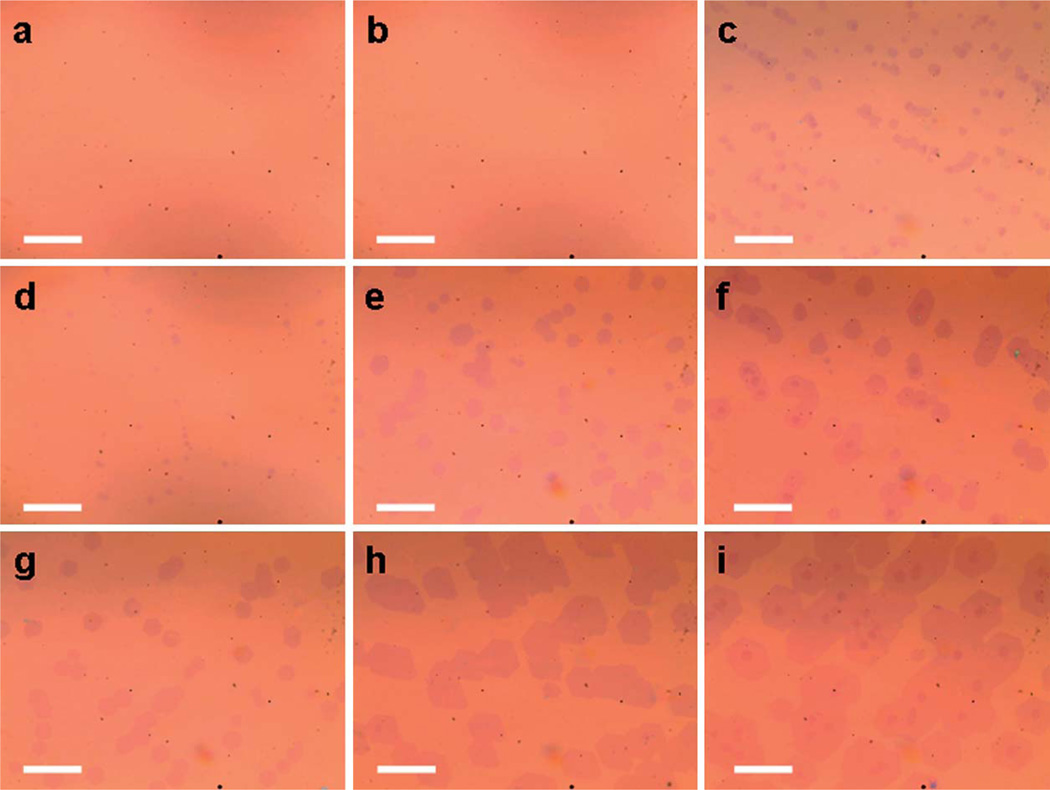
The effects of growth parameters, such as temperature and CH4 flow rate, on the size and density of domains were investigated in APCVD growth of graphene on a Cu substrate. In general, a Cu foil substrate (annealed at 1030–1070 °C) was used with a highly diluted hydrocarbon flow under ambient pressure (see Experimental section). Table 1 summarizes the detailed growth conditions of the graphene domains grown for 5 minutes. Nearly all the graphene domains have a hexagonal shape across the entire Cu foil, as shown by the optical microscopy (OM) images in Fig. 1. At a lower growth temperature and lower CH4 flow rate (lower CH4 partial pressure), no graphene domains were observed under an optical microscope (samples G1 and G2). With increasing temperature or CH4 partial pressure, hexagon shaped graphene domains appeared with different sizes and densities (G3–G9). With a further increase of temperature or CH4 partial pressure, the second layer domains start to appear (G3, G6, G8, and G9).
Fig. 1.
Optical images of graphene domains on 300 nm SiO2 obtained using different growth conditions summarized in Table 1: G1 (a), G2 (b), G3 (c), G4 (d), G5 (e), G6 (f), G7 (g), G8 (h), G9 (i); scale bars are 20 µm.
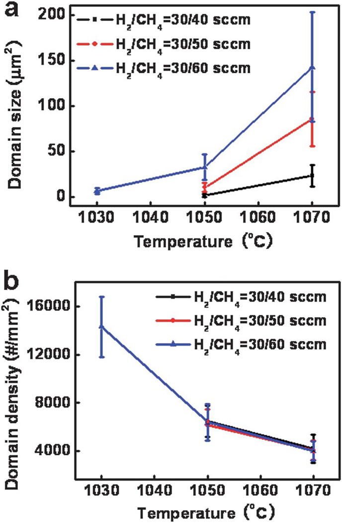
The changes in the average domain size and area density of the first layer domains are shown in Fig. 2. The average size of the graphene domains increases with the increasing growth temperature and CH4 partial pressure. The area domain density decreases with increasing temperature and is insensitive to the CH4 partial pressure. Overall, higher growth temperature yields a lower density of graphene nuclei with a larger domain size, while CH4 partial pressure only affects the graphene domain size. However, when the growth temperature and CH4 partial pressure are lower than a critical value, no domains can be seen by the OM (Fig. 1a and b). On the other hand, the second layer graphene domains start to appear when the temperature or CH4 partial pressure exceeds a critical point (Fig. 1c, f, h and i). In this way, there is only a limited window in which the graphene domains can maintain a monolayer structure (Fig. 1d, e, and g). These individual hexagonal domains can continuously grow and merge together to form a polycrystalline large-area graphene sheet with over 95% coverage of the total area (ESI, Fig. S1†). Additionally, the bilayer domains also showed hexagonal shape. Their size increases with increasing growth temperature and CH4 partial pressure.
Fig. 2.
Plots show (a) average size and (b) density of the first layer graphene domains, relative to the growth temperature and CH4 flow rate.
In general, the nucleation and growth of the graphene domains on Cu substrate is determined by the supersaturation of active carbon species derived from the decomposition of CH4, which is dependent on the growth temperature and CH4 partial pressure. In samples G1 and G2, the lack of graphene domains can be attributed to the undersaturation of carbon precursors on the Cu surface. On the other hand, when the supersaturation reaches a certain critical point at a higher temperature or higher CH4 partial pressure, nuclei can form on the Cu catalyst and grow into graphene domains that can continuously grow until they merge together with the neighboring domains to fully cover the entire Cu surface, as seen in samples G4, G5, and G7. Furthermore, second layer domains start to form if the supersaturation exceeds another critical point. The increase in the average size of the monolayer domains with increasing temperature and CH4 partial pressure can be attributed to a higher graphene growth speed due to the higher supersaturation of carbon-containing species.
The decrease in the area domain density with increasing temperature is counterintuitive at first glance, but can be fully interpreted after careful consideration of the nucleation and growth process. Generally, the initial graphene nuclei typically occur more frequently at step edges, folds, or other imperfections on the copper foil to form domains.18 Therefore, the presence and the number of monolayer domains highly depend on the surface condition of the Cu foil. With higher temperature annealing, the number of step edges, folds or other imperfections is reduced. Less steps and defects on the Cu surface lead to a lower density of nucleation sites and fewer domains. Additionally, a lower domain density at a higher growth temperature can also be attributed to an Ostwald ripening process during the initial growth stage. For example, the smoother Cu surface can enlarge the diffusion length of the carbon atoms. The longer diffusion length of carbon atoms increases the tendency of the Ostwald ripening, and therefore reduces the number of nucleates. Both these factors lead to a reduction of the graphene domain density at a higher temperature.
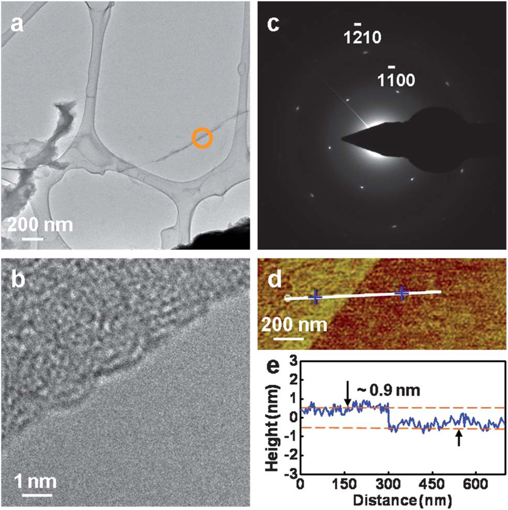
For electronic device applications, it is desirable to have large-area high quality graphene sheets without the presence of bilayer and non-uniform films. To achieve this, we prepared large-area graphene films using the growth condition of sample G5 for a longer growth duration (2 hours) (ESI, Fig. S1†). HRTEM of the graphene was performed to determine the film quality, as shown in Fig. 3a–c. Fig. 3a shows a suspended graphene transferred on a holy TEM grid, the edge of the graphene marked with an orange circle. The HRTEM image of the edge is shown in Fig. 3b. The selected area electron diffraction (SAED) pattern (Fig. 3c), with the zone axis of [0001], shows that the graphene is single crystalline. Furthermore, extensive SAED studies on an area over tens of square micrometres revealed that most regions of the graphene have a single set of hexagonal diffraction pattern of peaks, indicating the single-crystalline nature of the large domains. AFM was employed to determine the thickness of the as-grown graphene films (Fig. 3d and e). The height of the graphene with respect to the SiO2 substrate was found to be ~0.9 nm, which is consistent with the previous AFM observation of a single layer of graphene, and the larger than ideal 0.34 nm thickness can be attributed to substrate-graphene spacing.25,26 This single layer nature of the large-area graphene was further confirmed by Raman spectra and optical transmittance measurement (ESI, Fig. S1 and S2†).
Fig. 3.
(a) TEM image of graphene synthesized with mixed gas flow Ar : H2 : CH4 = 420 : 30 : 50 sccm under 1050 °C for 2 h, suspended on a holey carbon TEM grid, and the edge marked with an orange circle. (b) HRTEM image of the graphene corresponding to the edge in (a). (c) SAED pattern of the graphene at normal incidence. (d) AFM image of the as-grown graphene on SiO2 substrate, the central line indicates the section corresponding to the depth profile shown in (e), the height difference between the two dashed lines is ~0.9 nm, indicating monolayer graphene.
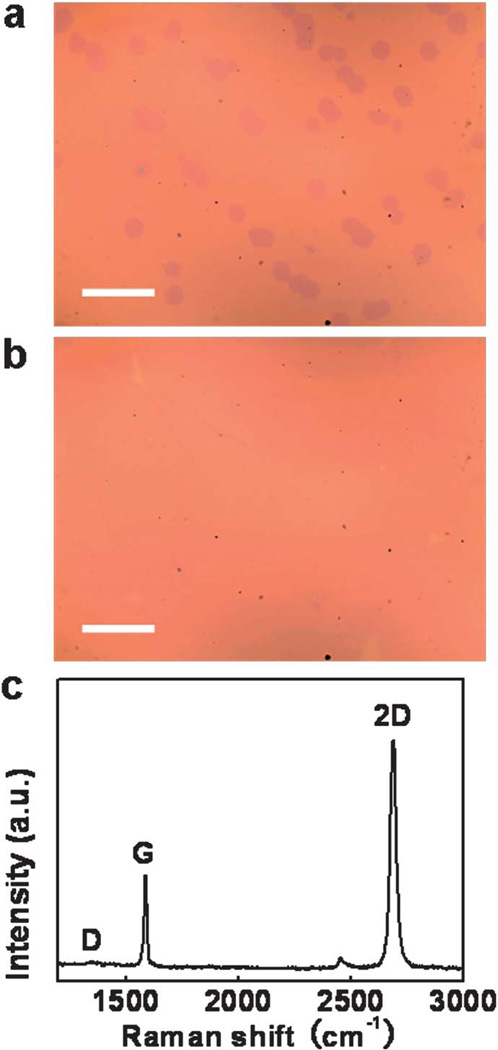
The presence of domain boundaries has been found to be detrimental to the fundamental electronic properties of graphene.14,27 Therefore, it is important to reduce the domain density and increase the domain size to reduce the number of domain boundaries, and thus improve the quality of the large-area monolayer graphene. Fig. 2b has revealed that the density of the first layer domains is mainly dependent on the surface condition of the Cu foil, rather than on the CH4 partial pressure. Furthermore, the density is also statistically constant after the initial nucleation stage (ESI, Fig. S1†). This result is similar to the previous observation in a LPCVD process.12 On the basis of these observations, we have developed an improved two-step process with a higher temperature annealing step followed by a lower temperature growth step (Table 2 and Fig. 4). In step 1, a high annealing temperature (1070 °C, not exceeding the melting point of Cu) was used to flatten the Cu foil surface to reduce domain density. In step 2, the temperature was decreased to a lower value (1050 °C) to ensure no second layer growth and therefore to obtain a uniform monolayer graphene sheet. Comparing samples G5 and G10 (5 min growth for both of them), the domain density decreased from ~6200 mm−2 to ~4300 mm−2 due to the high temperature annealing step, the average size of the domains increased slightly (10.66 µm2 vs. 15.34 µm2) (Table 2). Strikingly, the overall surface coverage is roughly the same (6%), suggesting that the overall coverage is dictated by supersaturation determined by the growth temperature and CH4 partial pressure. Importantly, no second layer domains appeared on sample G10 (Fig. 4a). Extending the growth time of sample G10 to 2 h, a large-area graphene film with over 95% coverage was obtained with excellent continuity and uniformity (Fig. 4b).
Table 2.
Graphene growth parameters of the improved two-step synthesis technique (G10) compared to the original process (G5)
| T/°C | Ar : H2 : CH4 /sccm | t/min | Average domain size/µm2 |
Average domain density/# mm−2 |
||
|---|---|---|---|---|---|---|
| G5 | Step 1 | 1050 | 470 : 30 | 60 | 10.66 | 6200 |
| Step 2 | 1050 | 420 : 30 : 50 | 5 | |||
| G10 | Step 1 | 1070 | 470 : 30 | 60 | 15.34 | 4300 |
| Step 2 | 1050 | 420 : 30 : 50 | 5 |
Fig. 4.
Optical images and micro-Raman spectrum of the graphene transferred onto 300 nm SiO2 substrates grown using the improved two-step process. Optical images: (a) sample G10; (b) large-area graphene prepared under the same growth condition of sample G10 for 2 h; scale bars are 20 µm. (c) Raman spectrum of the large-area graphene film in (b).
Raman spectroscopy was employed to further evaluate the quality of the large-area graphene synthesized by the improved two-step process. In the Raman spectrum (Fig. 4c), the D band around 1345 cm−1, corresponding to disorder-induced defect levels in graphene, showed very low intensity in the spectrum, suggesting the high quality of graphene. The other two clearly visible peaks centered at ~1586 cm−1 and ~2690 cm−1 correspond to the G and 2D bands, respectively. The Raman spectrum revealed a high intensity ratio of I2D/IG ~2.84 and a symmetric 2D peak with a full width at half maximum (FWHM) of ~38 cm−1, confirming the presence of high quality monolayer graphene.15,16
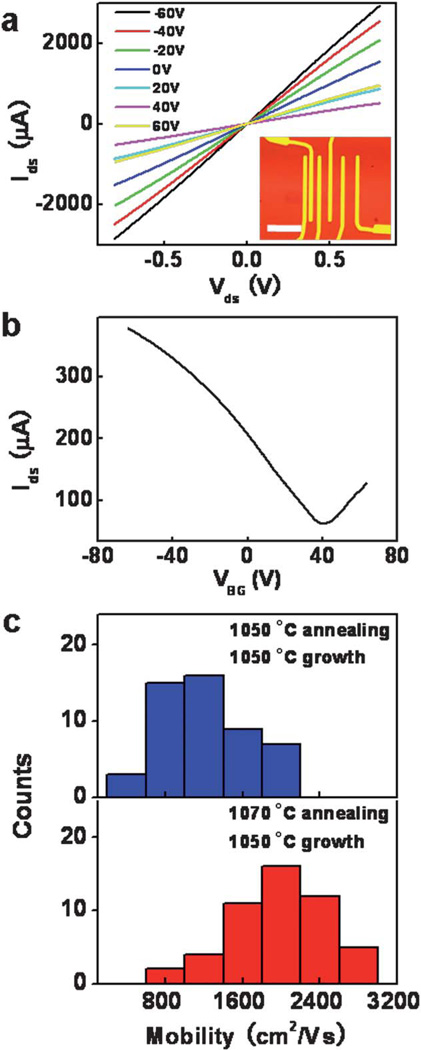
Transport measurements of graphene based field-effect transistors (FETs) were conducted to evaluate the electrical properties of the large-area graphene prepared with different annealing temperatures of 1050 °C and 1070 °C (Fig. 5). Fig. 5a shows a set of representative drain-source current (Ids) versus drain-source voltage (Vds) plots measured at room temperature. The Ids increases linearly with Vds. The inset shows an optical microscopy image of a typical device layout where the dark region in the center indicates a graphene strip patterned by oxygen plasma on a 300 nm SiO2/Si substrate. Fig. 5b shows representative drain-source current (Ids) versus the back-gated voltage (VBG) (Ids–VBG) curve. The effective mobility values were extracted using a standard model that takes contact resistance into account.20,28 Fig. 5c shows a summary of the mobility values distribution obtained from devices made of graphene from the original and improved synthetic processes. The values of hole mobility for graphene films obtained with 1050 °C annealing and 1050 °C growth ranges from 500 to about 2100 cm2 V−1 s−1. In contrast, the mobility for graphene grown using 1070 °C annealing and 1050 °C growth is significantly enhanced with a range of 850 to 3000 cm2 V−1 s−1. The observed carrier mobility are generally higher than the value ~400–600 cm2 V−1 s−1 reported previously on APCVD graphene,24 and nearly comparable to those reported for graphene grown by LPCVD, ranging from 800 cm2 V−1 s−1 to more than 5000 cm2 V−1 s−1.14,29 Obviously, higher quality graphene films are obtained from the improved two-step synthesis process, which provides a straightforward way to improve the film quality based on the fundamental understanding of the nucleation and growth of graphene domains in the APCVD process.
Fig. 5.
Representative room-temperature (a) Ids–Vds curves measured at various gate voltages (VBG = −60, −40, −20, 0, 20, 40, 60 V); (b) Ids–VBG curve measured at Vds = 0.1 V for the back-gated FET devices. Inset in (a) shows an optical image of the device; the scale bar is 20 µm. (c) A histogram of the carrier mobility distribution of the graphene prepared with the different synthetic processes.
Conclusions
In summary, large-area monolayer graphene was successfully grown on Cu foils using the APCVD method. We found that nucleation and growth of the domains was strongly dependent on the growth parameters: temperature and CH4 flow rate (partial pressure). The mean size of the domains increased with increasing growth temperature and CH4 partial pressure, while the density of domains decreased with increasing growth temperature and was independent of the CH4 partial pressure. A systematic study reveals that the domain density is highly dependent on the initial annealing process. An improved two-step synthesis process with higher initial annealing temperature but lower growth temperature helps achieve a high quality full-surface coverage of monolayer graphene films. Electrical transport measurements showed that the carrier mobility of the optimized graphene films can reach up to ~3000 cm2 V−1 s−1 at room temperature. This research should be beneficial for both the fundamental understanding of the graphene growth mechanism and the development of graphene based devices.
Acknowledgements
We acknowledge the Electron Imaging Center for Nanomachines (EICN) at UCLA for the technical support of TEM. We are also grateful to Professor Yang Yang for allowing us to use the Raman microscope in his lab at CNSI. H. Z. and X.D. are grateful to Camille and Henry Dreyfus Foundation for financial support through the Camille and Henry Dreyfus Postdoctoral Program in Environmental Chemistry. X.D. acknowledges financial support by NSF CAREER award 0956171. Y.H. acknowledges support by the NIH Director’s New Innovator Award Program, part of the NIH Roadmap for Medical Research, through Grant 1DP2OD007279 (Y.H.).
Footnotes
Electronic supplementary information (ESI) available: Time dependence of graphene coverage on Cu foil and their Raman spectra, and transmittance spectrum of the large-area graphene film transferred on a glass plate. See DOI: 10.1039/c1jm14272k
Contributor Information
Yu Huang, Email: yhuang@seas.ucla.edu.
Xiangfeng Duan, Email: xduan@chem.ucla.edu.
Notes and references
- 1.Bolotin KI, Sikes KJ, Jiang Z, Klima M, Fudenberg G, Hone J, Kim P, Stormer HL. Solid State Commun. 2008;146:351. [Google Scholar]
- 2.Balandin AA, Ghosh S, Bao WZ, Calizo I, Teweldebrhan D, Miao F, Lau CN. Nano Lett. 2008;8:902. doi: 10.1021/nl0731872. [DOI] [PubMed] [Google Scholar]
- 3.Lee C, Wei X, Kysar JW, Hone J. Science. 2008;321:385. doi: 10.1126/science.1157996. [DOI] [PubMed] [Google Scholar]
- 4.Liao L, Lin Y-C, Bao M, Cheng R, Bai J, Liu Y, Qu Y, Wang KL, Huang Y, Duan XF. Nature. 2010;467:305. doi: 10.1038/nature09405. [DOI] [PMC free article] [PubMed] [Google Scholar]
- 5.Liu N, Luo F, Wu H, Liu Y, Zhang C, Chen J. Adv. Funct. Mater. 2008;18:1518. [Google Scholar]
- 6.Williams G, Seger B, Kamat PV. ACS Nano. 2008;2:1487. doi: 10.1021/nn800251f. [DOI] [PubMed] [Google Scholar]
- 7.Wang H, Robinson JT, Li X, Dai H. J. Am. Chem. Soc. 2009;131:9910. doi: 10.1021/ja904251p. [DOI] [PubMed] [Google Scholar]
- 8.Liao KH, Mittal A, Bose S, Leighton C, Mkhoyan KA, Macosko CW. ACS Nano. 2011;5:1253. doi: 10.1021/nn1028967. [DOI] [PubMed] [Google Scholar]
- 9.Lin Y-M, Dimitrakopoulos C, Jenkins KA, Farmer DB, Chiu HY, Grill A, Avouris P. Science. 2010;327:662. doi: 10.1126/science.1184289. [DOI] [PubMed] [Google Scholar]
- 10.Reina A, Jia X, Ho J, Nezich D, Son H, Bulovic V, Dresselhaus MS, Kong J. Nano Lett. 2009;9:30. doi: 10.1021/nl801827v. [DOI] [PubMed] [Google Scholar]
- 11.Kim KS, Zhao Y, Jang H, Lee SY, Kim JM, Kim KS, Ahn JH, Kim P, Choi JY, Hong BH. Nature. 2009;457:706. doi: 10.1038/nature07719. [DOI] [PubMed] [Google Scholar]
- 12.Li X, Cai W, An J, Kim S, Nah J, Yang D, Piner R, Velamakanni A, Jung I, Tutuc E, Banerjee SK, Colombo L, Ruoff RS. Science. 2009;324:1312. doi: 10.1126/science.1171245. [DOI] [PubMed] [Google Scholar]
- 13.Wofford JM, Nie S, McCarty KF, Bartelt NC, Dubon OD. Nano Lett. 2010;10:4890. doi: 10.1021/nl102788f. [DOI] [PubMed] [Google Scholar]
- 14.Li X, Magnuson CW, Venugopal A, An J, Suk JW, Han B, Borysiak M, Cai W, Velamakanni A, Zhu Y, Fu L, Vogel EM, Voelkl E, Colombo L, Ruoff RS. Nano Lett. 2010;10:4328. doi: 10.1021/nl101629g. [DOI] [PubMed] [Google Scholar]
- 15.Liu N, Fu L, Dai B, Yan K, Liu X, Zhao RQ, Zhang YF, Liu ZF. Nano Lett. 2011;11:297. doi: 10.1021/nl103962a. [DOI] [PubMed] [Google Scholar]
- 16.Bhaviripudi S, Jia X, Dresselhaus MS, Kong J. Nano Lett. 2011;10:4128. doi: 10.1021/nl102355e. [DOI] [PubMed] [Google Scholar]
- 17.Yao Y, Li Z, Lin Z, Moon K-S, Agar J, Wong C. J. Phys. Chem. C. 2011;115:5232. [Google Scholar]
- 18.Robertson AW, Warner JH. Nano Lett. 2011;11:1182. doi: 10.1021/nl104142k. [DOI] [PubMed] [Google Scholar]
- 19.Sutter PW, Flege JI, Sutter EA. Nat. Mater. 2008;7:406. doi: 10.1038/nmat2166. [DOI] [PubMed] [Google Scholar]
- 20.Kim S, Nah J, Jo I, Shahrjerdi D, Colombo L, Yao Z, Tutuc E, Banerjee SK. Appl. Phys. Lett. 2009;94 062107. [Google Scholar]
- 21.Meric I, Han MY, Young AF, Ozyilmaz B, Kim P, Shepard KL. Nat. Nanotechnol. 2008;3:654. doi: 10.1038/nnano.2008.268. [DOI] [PubMed] [Google Scholar]
- 22.Yan K, Peng H, Zhou Y, Li H, Liu Z. Nano Lett. 2011;11:1106. doi: 10.1021/nl104000b. [DOI] [PubMed] [Google Scholar]
- 23.Li X, Magnuson CW, Venugopal A, Tromp RM, Hannon JB, Vogel EM, Colombo L, Ruoff RS. J. Am. Chem. Soc. 2011;133:2816. doi: 10.1021/ja109793s. [DOI] [PubMed] [Google Scholar]
- 24.Luo Z, Lu Y, Singer DW, Berck ME, Somers LA, Goldsmith BR, Johnson ATC. Chem. Mater. 2011;23:1441. [Google Scholar]
- 25.Novoselov KS, Geim AK, Morozov SV, Jiang D, Zhang Y, Dubonos SV, Grigorieva IV, Firsov AA. Science. 2004;306:666. doi: 10.1126/science.1102896. [DOI] [PubMed] [Google Scholar]
- 26.Nemes-Incze P, Osváth Z, Kamarás K, Biró LP. Carbon. 2008;46:1435. [Google Scholar]
- 27.Yu Q, Jauregui LA, Wu W, Colby R, Tian J, Su Z, Cao H, Liu Z, Pandey D, Wei D, Chung TF, Peng P, Guisinger NP, Stach EA, Bao J, Pei SS, Chen YP. Nat. Mater. 2011;10:443. doi: 10.1038/nmat3010. [DOI] [PubMed] [Google Scholar]
- 28.Liao L, Bai J, Qu Y, Lin Y, Li Y, Huang Y, Duan X. Proc. Natl. Acad. Sci. U. S. A. 2010;107:6711. doi: 10.1073/pnas.0914117107. [DOI] [PMC free article] [PubMed] [Google Scholar]
- 29.Huang PY, Ruiz-Vargas CS, van der Zande AM, Whitney WS, Levendorf MP, Kevek JW, Garg S, Alden JS, Hustedt CJ, Zhu Y, Park J, McEuen PL, Muller DA. Nature. 2011;469:389. doi: 10.1038/nature09718. [DOI] [PubMed] [Google Scholar]


