Abstract
The electrochemical growth of zinc oxide (ZnO) nanostructures on graphene on glass using zinc nitrate hexahydrate was studied. The effects of current densities and temperatures on the morphological, structural, and optical properties of the ZnO structures were studied. Vertically aligned nanorods were obtained at a low temperature of 75°C, and the diameters increased with current density. Growth temperature seems to have a strong effect in generating well-defined hexagonal-shape nanorods with a smooth top edge surface. A film-like structure was observed for high current densities above -1.0 mA/cm2 and temperatures above 80°C due to the coalescence between the neighboring nanorods with large diameter. The nanorods grown at a temperature of 75°C with a low current density of -0.1 mA/cm2 exhibited the highest density of 1.45 × 109 cm-2. X-ray diffraction measurements revealed that the grown ZnO crystallites were highly oriented along the c-axis. The intensity ratio of the ultraviolet (UV) region emission to the visible region emission, IUV/IVIS, showed a decrement with the current densities for all grown samples. The samples grown at the current density below -0.5 mA/cm2 showed high IUV/IVIS values closer to or higher than 1.0, suggesting their fewer structural defects. For all the ZnO/graphene structures, the high transmittance up to 65% was obtained at the light wavelength of 550 nm. Structural and optical properties of the grown ZnO structures seem to be effectively controlled by the current density rather than the growth temperature. ZnO nanorod/graphene hybrid structure on glass is expected to be a promising structure for solar cell which is a conceivable candidate to address the global need for an inexpensive alternative energy source.
Keywords: Electrochemical deposition, Graphene, Nanorod, Zinc oxide, Solar cell, Hybrid structure
Background
In recent years, the hybrid structures of zinc oxide (ZnO) nanostructures on graphene have attracted much attention because the nanostructures can offer additional functionalities to graphene for realizing advanced nanoscale applications [1,2]. This is due to the superior properties of nanostructures such as quantum confinement effects and high surface-to-volume ratio [3]. ZnO nanostructures on graphene on glass is expected to be a promising structure for solar cell which is a viable candidate to address the global need for an inexpensive alternative energy source [4]. Recently, ZnO has been shown to be able to enhance the power conversion efficiency of conjugated polymer-based solar cells [5,6]. Typically, the electrode of a solar cell is formed by the transparent conductive oxides such as fluorine-doped tin oxide (FTO) or indium tin oxide (ITO) deposited on glass [4,7]. However, FTO and ITO are expensive and non-flexible in contrast to graphene which is cheap and flexible. In ZnO/graphene/glass-based solar-cell-structure system, graphene is expected to act as an excellent conducting transparent electrode material [8,9] because of its extraordinary electrical, thermal, and mechanical properties including a carrier mobility exceeding 104 cm2/Vs and a thermal conductivity of 103 W/mK [10-13]. Interestingly, the direct growth of ZnO nanorods on graphene with high crystallinity and uniformity has also been reported in several literatures so far [1,2,14,15]. Therefore, the ZnO/graphene/glass system can be regarded as one of the most conceivable candidates for solar cell application.
The growth of ZnO nanostructures on graphene can be performed either by vapor-phase method [1,4,16] or by liquid-phase method [2,15,17,18]. In general, the former is likely to involve high temperature and is also considered as a high-cost method. Moreover, in many cases, the vapor-phase method requires oxygen gas. There is a possibility that graphene is oxidized or etched out during the growth of the ZnO nanostructures because the oxidation of graphene occurs at temperature as low as 450°C [19]. On the other hand, the liquid-phase method such as electrochemical deposition has advantages over the vapor-phase method because of its simplicity, low cost, and low process temperature [20]. In addition, this method gives good controllability of both growth rate and structure dimension. In this paper, we report the effects of current density and growth temperature on morphological, structural, and optical properties of ZnO structures grown on monolayer graphene/glass by electrochemical deposition without using any supporting reagent.
Methods
A monolayer graphene on glass (Graphene Laboratories Inc., Calverton, NY, USA) was used as a substrate to grow ZnO nanostructures. The electrochemical deposition process was carried out using cathodic electrochemical deposition utilizing two electrodes of which a platinum (Pt) wire acts as an anode and a monolayer graphene as a cathode. The schematic diagram of the experimental setup is illustrated in Figure 1a. Zinc nitrate hexahydrate (Zn(NO3)2.6H2O) (Sigma-Aldrich (St. Louis, MO, USA), ≥99.0% purity) solution (10 mM) without any supporting agent was used as an electrolyte. The growth was done at current densities of -0.1, -0.5, -1.0, -2.0, and -3.0 mA/cm2 and temperatures of 75°C, 80°C, and 90°C for 45 min. The graphene/glass substrates were immersed into the electrolyte immediately after reaching the setting temperatures, i.e., 75°C, 80°C, and 90°C. The time chart of the growth is shown in Figure 1b. The grown structures were characterized using field-emission scanning electron microscopy (FESEM, Hitachi SU8030, Hitachi Ltd., Chiyoda-ku, Japan), energy dispersive X-ray (EDX) spectroscopy, X-ray diffraction (XRD, Rigaku RINT 2100, Rigaku, Shibuya-ku, Japan), photoluminescence (PL) spectroscopy (Horiba Jobin Yvon, Horiba Ltd., Tokyo, Japan), and UV–vis spectrometer (Cary 5000, Agilent Technologies, Inc., Santa Clara, CA, USA).
Figure 1.
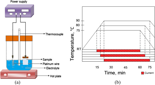
Schematic diagram of the experimental setup and time chart. (a) Schematic diagram of electrochemical deposition setup and (b) growth time chart.
Results and discussion
At first, it is worth to describe the chemical reactions that take place during the growth of ZnO structures on graphene [15]. As shown by Equation 1, Zn(NO3)2 decomposes to Zn ions (Zn2+) and nitrate ions (NO3 -). Hydroxide ions (OH-) are produced during the reduction process of the water (H2O) with NO3 - ions (Equation 2). Then, OH- reacts with Zn2+ to form the complex compound, Zn(OH)2 (Equation 3). Finally, the formed Zn(OH)2 continues to dihydrate into ZnO with the presence of heat. While at the anode, water is oxidized to produce hydrogen ions (H+).
Cathode:
| (1) |
| (2) |
| (3) |
| (4) |
Anode:
| (5) |
Figure 2 shows the top view FESEM images together with the corresponding EDX spectra of the grown ZnO structures on graphene at temperatures of 75°C, 80°C, and 90°C with current densities of -0.1, -1.0, and -3.0 mA/cm2. It can be seen that the morphologies of the structures seem to be strongly dependent on both applied current density and temperature. At the low temperature of 75°C, the growth of vertically aligned ZnO nanorods was observed as shown in Figure 2a,b,c. The diameters of the grown nanorods increase with the current densities. This is presumably due to the higher current density leading to a rapid formation of OH- ions at the surface of graphene which then may result in much denser and larger seeds in the early stage of the growth process [14]. The grown nanorods show considerably good hexagonal-shape structure, but the top end surfaces of nanorods are likely to be rough. At the temperature of 80°C, it can be seen that well-defined hexagonal-shape nanorods with smooth top end surfaces were obtained for the current density of -0.1 mA/cm2. When the current density increases from -0.1 to -1.0 mA/cm2, the diameters of nanorods increase, resulting in the formation of film-like structures due to the coalescences between the neighboring nanorods with large diameter. Well-defined hexagonal-shape structures were also observed at temperature of 90°C for the low current density of -0.1 mA/cm2. These results suggest that a high growth temperature promotes the generation of the well-defined hexagonal shape of nanorods without using supporting reagents such as hexamethylenetetramine (HMTA) [2]. The coalescences between the neighboring nanorods observed on the samples grown at the current densities above -1.0 mA/cm2 are due to the increase in the diameters of nanorods. From the analysis of the EDX spectra, only zinc (Zn), oxygen (O) and carbon (C) elements were detected in all the grown samples and the total compositional atomic percentages of Zn and O were estimated to be above 95%. Table 1 summarizes the morphological structures, densities, and diameters of the grown nanostructures including comparison with other works which were also performed on graphene. In this study, the nanorods grown at the low temperature of 75°C with low current density of -0.1 mA/cm2 exhibited the highest nanorod density of 1.45 × 109 cm-2. This value is one order higher than that of the work reported by Xu et al. [14]. Here, the nanorods were also grown using the similar technique, electrolyte, and current density but at a higher temperature of 90°C. Moreover, our highest nanorod density is two orders higher than that of nanorods grown in a mixture of zinc nitrate and HMTA by hydrothermal process as reported by Kim et al. [18]. Again, this density is in the same order with the nanorods grown in a mixture of zinc nitrate and HMTA at a bit higher current density of -0.5 mA/cm2 and a higher temperature of 80°C using an electrochemical deposition as reported by Aziz et al. [2]. Furthermore, our highest nanorod density was also found to be in the same order with nanorods grown at 800°C by thermal evaporation [1] and with nanoneedles grown at 400°C by metal-organic vapor-phase epitaxy (MOVPE) [16].
Figure 2.
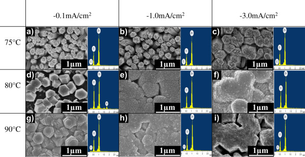
FESEM images and EDX spectra of ZnO nanostructures. Top view of FESEM images and EDX spectra of ZnO nanostructures grown with different current densities at temperatures of (a-c) 75°C, (d-f) 80°C, and (g-i) 90°C.
Table 1.
Density and diameter of the grown ZnO nanorods
| Method | Temperature,°C | Current density, mA/cm 2 | Electrolyte/source | Density, cm -2 | Diameter of nanorods, nm | Morphological structure |
|---|---|---|---|---|---|---|
| Electrochemical deposition (this work) |
75 |
-0.1 |
Zinc nitrate solution |
1.45 × 10⁹ |
100 to 275 |
Nanorods |
| -0.5a |
8.09 × 10⁸ |
225 to 575 |
Nanorods |
|||
| -1.0 |
1.24 × 10⁹ |
100 to 325 |
Nanorods |
|||
| -2.0a |
3.53 × 10⁸ |
200 to 825 |
Nanorods |
|||
| -3.0 |
7.47 × 10⁸ |
250 to 500 |
Nanorods |
|||
| 80 |
-0.1 |
5.60 × 10⁸ |
243 to 500 |
Nanorods |
||
| -1.0 |
- |
- |
Film-like structure |
|||
| -3.0 |
- |
- |
Film-like structure |
|||
| 90 |
-0.1 |
6.22 × 10⁸ |
214 to 500 |
Nanorods |
||
| -1.0 |
- |
- |
Film-like structure |
|||
| -3.0 |
- |
- |
Film-like structure |
|||
| Electrochemical deposition [14] |
90 |
-0.15 |
Zinc nitrate solution |
5.83 × 10⁸ |
370 to 780 |
Nanorods |
| Electrochemical deposition [2] |
80 |
-0.1 |
Zinc nitrate solution and HMTA |
1.84 × 10⁷ |
190 to 450 |
Nanorods |
| -0.5 |
1.37 × 10⁹ |
260 to 480 |
Nanorods |
|||
| -1.0 |
1.24 × 10⁸ |
660 to 1,000 |
Nanorods |
|||
| -1.5 |
3.42 × 10⁷ |
950 to 1,330 |
Nanocrystal |
|||
| -2.0 |
2.32 × 10⁷ |
570 to 2,030 |
Rods |
|||
| Hydrothermal process [18] |
60 |
- |
Zinc nitrate solution and HMTA |
3.10 × 10⁷ |
710 |
Nanorods |
| 80 |
- |
3.00 × 10⁷ |
680 |
Nanorods |
||
| 95 |
- |
4.20 × 10⁷ |
690 |
Nanorods |
||
| Thermal evaporation [1] |
600 |
- |
Zn powder and oxygen gas |
- |
- |
Nanocluster |
| 800 |
- |
6.86 × 10⁹ |
50 to 150 |
Nanorods |
||
| 1,000 |
- |
- |
- |
Thin film |
||
| Metal-organic vapor-phase epitaxy (MOVPE) [16] |
400 |
- |
Diethylzinc (DEZn) and oxygen gas |
4.00 × 10⁹ |
100 ± 10 |
Nanoneedles |
| 600 |
- |
|
8.00 × 10⁷ |
90 ± 20 |
Nanoneedles |
|
| 750 | - | 5.00 × 10⁷ | Not stated | Nanoneedles |
aSEM data not shown.
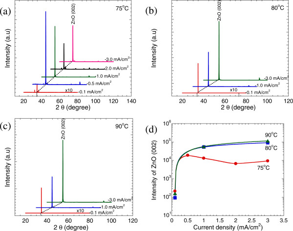
Figure 3a,b,c shows the XRD spectra of the nanorods grown at different current densities and temperatures. All observed reflection peaks can be indexed to the hexagonal wurtzite phase of ZnO (JCPDS card no. 36–1451). It can be clearly seen that the intensity of the (002) diffraction peak is much stronger than the other peaks for all samples indicating that these as-grown ZnO structures are highly oriented along the c-axis. Figure 3d shows the intensity of ZnO (002) as a function of current density for temperatures of 75°C, 80°C, and 90°C. It is well known that the intensity of the diffraction peak has a close connection with the thickness of the measured structure. Therefore, the reason why the intensities for the samples grown at 75°C are low and do not show significant changes for all current densities is probably their thin layer thicknesses or nanorod structures. For both temperatures of 80°C and 90°C, the intensity of the ZnO (002) peak increases drastically with the current density, suggesting that the thicknesses of grown structures are relatively thick and the thicknesses increase with the current density. However, the differences between the intensities of ZnO (002) for the sample grown at 80°C and those for the samples grown at 90°C are very small, suggesting the lesser effect of temperature in promoting the thicknesses of the grown structures.
Figure 3.
XRD spectra of the grown ZnO structures with different applied current densities and temperatures. XRD spectra of the grown ZnO structures with different applied current densities at temperatures of (a) 75°C, (b) 80°C, and (c) 90°C. (d) Current density vs. intensity of the ZnO (002) peak.
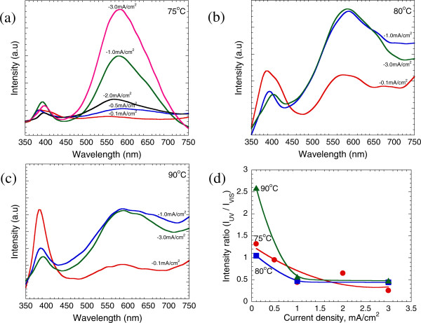
The optical characteristics of ZnO were investigated using room temperature (RT) PL spectroscopy. Figure 4a,b,c shows the PL spectra of the ZnO nanostructures deposited on the graphene layers at temperatures of 75°C, 80°C, and 90°C with different applied current densities, respectively. Two distinct emission bands can be seen: one of which is located in the wavelength range of 382 to 402 nm of the ultraviolet (UV) region, and the other is located in the wavelength range of 565 to 589 nm of the visible region. This former is known as the near-band-edge (NBE) emission and could be referred to as an intrinsic property of the wurtzite crystal structure of ZnO and originated from the excitonic recombination [21]. On the other hand, the latter has been reported to be due to the radiative recombination of photon-generated holes with a single ionized charge of specific defects such as O vacancies or Zn interstitials [22]. Figure 4d summarizes the PL intensity ratio of the UV region emission to the visible region emission, denoted by IUV/IVIS, as a function of current density. Regardless of the difference in growth temperature, the IUV/IVIS values decrease linearly with the increase in current density from -0.1 to -1.0 mA/cm2 for all temperatures, whereas those values are almost unchanged in the range from -1.0 to -3.0 mA/cm2. The IUV/IVIS values for the samples grown at the current densities of -0.1 and -0.5 mA/cm2 are closer to or larger than 1.0. The highest ratio of 2.5 is obtained on the sample grown at the temperature of 90°C and current density of -0.1 mA/cm2. In general, the higher the IUV/IVIS value, the fewer the structural defects in the grown structures [23,24].
Figure 4.
PL spectra of the grown ZnO structures with different applied current densities and temperatures. PL spectra of the grown ZnO structures with different applied current densities at temperatures of (a) 75°C, (b) 80°C, and (c) 90°C. (d) Current density vs. PL intensity ratio, IUV/IVIS.
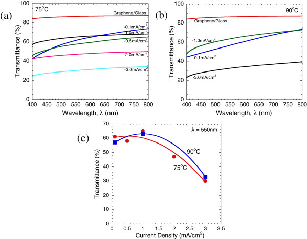
Figure 5a,b shows the optical transmittance spectra of ZnO structures grown at 75°C and 90°C, respectively. Figure 5c shows the relation between the current density and the transmittance at the wavelength of 550 nm. The samples grown at low current densities (below -1.0 mA/cm2) exhibit high transmittance values up to 65% due to their thin structures, whereas those grown at high current densities show low transmittance values due to their thick structures. No significant difference between the samples grown at the low temperature of 75°C and those grown at the high temperature of 90°C seems likely to prove a lesser effect of temperature on the thickness. The highly transparent ZnO/graphene hybrid structure is expected to be applicable for the fabrication of solar cell device as well as for other kinds of transparent optoelectronic devices [13].
Figure 5.
Optical transmittance of the ZnO structures. Optical transmittance of the ZnO structures grown at (a) 75°C and (b) 90°C with different applied current densities. (c) Current density vs. transmittance at wavelength of 550 nm.
Conclusions
The effects of current density and temperature on the morphological, structural, and optical properties of ZnO grown on graphene were studied. Vertically aligned nanorods were obtained at low growth temperatures. Growth temperature has a close connection with the appearance of the well-defined hexagonal-shape nanorods with smooth top end surface. A film-like structure caused by the coalescences between the neighboring nanorods with large diameters was observed on the samples grown at high current densities and high temperatures. The nanorods grown at a low temperature and low current density tended to exhibit a high density of nanorod. The XRD measurements revealed that the grown ZnO structures were highly oriented along the c-axis. The samples grown at low current densities seem to show fewer structural defects in the grown structures. The ZnO/graphene structures exhibited high transmittance values up to 65% at the light wavelength of 550 nm. ZnO nanorod/graphene hybrid structure on glass is expected to be a promising structure for solar cell which is a viable candidate to address the global need for an inexpensive alternative energy source.
Competing interests
The authors declare that they have no competing interests.
Authors’ contributions
NAH and HY designed and performed the experiments; participated in the characterization and data analysis of FESEM, XRD, PL and UV–vis; and prepared the manuscript. MRM participated in the PL and UV–vis characterization. TT participated in the XRD characterization and revision of the manuscript. AMH participated in the monitoring of the experimental work, data analysis, discussion, and revision of the manuscript. All authors read and approved the final manuscript.
Contributor Information
Nur Ashikyn Hambali, Email: shikynhambali@gmail.com.
Hafizal Yahaya, Email: hafizal.kl@utm.my.
Mohamad Rusop Mahmood, Email: nanouitm@gmail.com.
Tomoaki Terasako, Email: erasako.tomoaki.mz@ehime-u.ac.jp.
Abdul Manaf Hashim, Email: abdmanaf@utm.my.
Acknowledgements
NAH thanks the Malaysia-Japan International Institute of Technology for the scholarship. This work was funded by Nippon Sheet Glass Corp., Hitachi Foundation, Malaysia-Japan International Institute of Technology, Universiti Teknologi Malaysia, Malaysia Ministry of Science, Technology and Innovation, and Malaysia Ministry of Education.
References
- Ahmad NF, Rusli NI, Mahmood MR, Yasui K, Hashim AM. Seed/catalyst-free growth of zinc oxide nanostructures on multilayer graphene by thermal evaporation. Nanoscale Res Lett. 2014;9:83–89. doi: 10.1186/1556-276X-9-83. [DOI] [PMC free article] [PubMed] [Google Scholar]
- Aziz NSA, Mahmood MR, Yasui K, Hashim AM. Seed/catalyst-free vertical growth of high-density electrodeposited zinc oxide nanostructures on a single-layer graphene. Nanoscale Res Lett. 2014;9:95–102. doi: 10.1186/1556-276X-9-95. [DOI] [PMC free article] [PubMed] [Google Scholar]
- Kar JP, Das SN, Lee SW, Ham MH, Choi J, Myoung JM. Surface modifications of hydrothermally grown ZnO nanostructures with process parameters. Chem Eng Commun. 2009;196:1130–1138. doi: 10.1080/00986440902897491. [DOI] [Google Scholar]
- Yu D, Trad T, McLeskey JT, Craciun V, Taylor CR. ZnO nanowires synthesized by vapor phase transport deposition on transparent oxide substrates. Nanoscale Res Lett. 2010;5:1333–1339. doi: 10.1007/s11671-010-9649-3. [DOI] [PMC free article] [PubMed] [Google Scholar]
- Beek WJE, Wienk MM, Janssen RAJ. Efficient hybrid solar cells from zinc oxide nanoparticles and a conjugated polymer. Adv Mater. 2004;16:1009–1013. doi: 10.1002/adma.200306659. [DOI] [Google Scholar]
- Unalan HE, Hiralal P, Kuo D, Parekh B, Amaratunga G, Chhowalla M. Flexible organic photovoltaics from zinc oxide nanowires grown on transparent and conducting single walled carbon nanotube thin films. J Mater Chem. 2008;18:5909–5912. doi: 10.1039/b810748c. [DOI] [Google Scholar]
- She GW, Zhang XH, Shi WS, Fan X, Chang JC, Lee CS, Lee ST, Liu CH. Controlled synthesis of oriented single-crystal ZnO nanotube arrays on transparent conductive substrates. Appl Phys Lett. 2008;92:053111. doi: 10.1063/1.2842386. [DOI] [Google Scholar]
- Wang X, Zhi L, Mullen K. Transparent, conductive graphene electrodes for dye-sensitized solar cells. Nano Lett. 2008;8:323–327. doi: 10.1021/nl072838r. [DOI] [PubMed] [Google Scholar]
- Eda G, Fanchini G, Chhowalla M. Large-area ultrathin films of reduced graphene oxide as a transparent and flexible electronic material. Nat Nanotechnol. 2008;3:270–274. doi: 10.1038/nnano.2008.83. [DOI] [PubMed] [Google Scholar]
- Novoselov KS, Geim AK, Morozov SV, Jiang D, Katsnelson MI, Grigorieva IV, Dubonos SV, Firsov AA. Two-dimensional gas of massless Dirac fermions in graphene. Nature. 2005;438:197–200. doi: 10.1038/nature04233. [DOI] [PubMed] [Google Scholar]
- Zhang Y, Tan Y-W, Stormer HL, Kim P. Experimental observation of the quantum Hall effect and Berry's phase in graphene. Nature. 2005;438:201–204. doi: 10.1038/nature04235. [DOI] [PubMed] [Google Scholar]
- Kim KS, Zhao Y, Jang H, Lee SY, Kim JM, Kim KS, Ahn J-H, Kim P, Choi J-Y, Hong BH. Large-scale pattern growth of graphene films for stretchable transparent electrodes. Nature. 2009;457:706–710. doi: 10.1038/nature07719. [DOI] [PubMed] [Google Scholar]
- Balandin AA, Ghosh S, Bao W, Calizo I, Teweldebrhan D, Miao F, Lau CN. Superior thermal conductivity of single-layer graphene. Nano Lett. 2008;8(3):902–907. doi: 10.1021/nl0731872. [DOI] [PubMed] [Google Scholar]
- Xu C, Lee J-H, Lee J-C, Kim B-S, Hwang SW, Whang D. Electrochemical growth of vertically aligned ZnO nanorod arrays on oxidized bi-layer graphene electrode. Cryst Eng Comm. 2011;13(20):6036–6039. doi: 10.1039/c1ce05695f. [DOI] [Google Scholar]
- Xu C, Kim B-S, Lee J-H, Kim M, Hwang SW, Choi BL, Lee EK, Kim JM, Whang D. Seed-free electrochemical growth of ZnO nanotube arrays on single-layer graphene. Mater Lett. 2012;72:25–28. [Google Scholar]
- Kim Y-J, Lee J-H, Yi G-C. Vertically aligned ZnO nanostructures grown on graphene layers. Appl. 2009;95:213101. doi: 10.1063/1.3266836. [DOI] [Google Scholar]
- Aziz NSA, Nishiyama T, Rusli NI, Mahmood MR, Yasui K, Hashim AM. Seedless growth of zinc oxide flower-shaped structures on multilayer graphene by electrochemical deposition. Nanoscale Res Lett. 2014;9:337–345. doi: 10.1186/1556-276X-9-337. [DOI] [PMC free article] [PubMed] [Google Scholar]
- Kim Y-J, Hadiyawarman, Yoon A, Kim M, Yi G-C, Liu C. Hydrothermally grown ZnO nanostructures on few-layer graphene sheets. Nanotechnology. 2011;22(24):245603. doi: 10.1088/0957-4484/22/24/245603. [DOI] [PubMed] [Google Scholar]
- Liu L, Ryu S, Tomasik MR, Stolyarova E, Jung N, Hybertsen MS, Steigerwald ML, Brus LE, Flynn GW. Graphene oxidation: thickness-dependent etching and strong chemical doping. Nano Lett. 2008;8:1965–1970. doi: 10.1021/nl0808684. [DOI] [PubMed] [Google Scholar]
- Izaki M, Omi T. Transparent zinc oxide films prepared by electrochemical reaction. Appl Phys Lett. 1996;68:2439–2440. doi: 10.1063/1.116160. [DOI] [Google Scholar]
- Mahmood K, Park SS, Sung HJ. Enhanced photoluminescence, Raman spectra and field-emission behavior of indium-doped ZnO nanostructures. J Mater Chem C. 2013;1:3138–3149. doi: 10.1039/c3tc00082f. [DOI] [Google Scholar]
- Rusli NI, Tanikawa M, Mahmood MR, Yasui K, Hashim AM. Growth of high-density zinc oxide nanorods on porous silicon by thermal evaporation. Materials. 2012;5:2817–2832. doi: 10.3390/ma5122817. [DOI] [Google Scholar]
- Ghosh M, Raychaudhuri AK. Shape transition in ZnO nanostructures and its effect on blue-green photoluminescence. Nanotechnology. 2008;19:1–7. doi: 10.1088/0957-4484/19/44/445704. [DOI] [PubMed] [Google Scholar]
- Xu XL, Lau SP, Chen JS, Chen GY, Tay BK. Polycrystalline ZnO thin films on Si(100) deposited by filtered cathodic vacuum arc. J Cryst Growth. 2001;223:201–205. doi: 10.1016/S0022-0248(01)00611-X. [DOI] [Google Scholar]


