Abstract
In this work, we propose Silicon based broad-band near infrared Schottky barrier photodetectors. The devices operate beyond 1200 nm wavelength and exhibit photoresponsivity values as high as 3.5 mA/W with a low dark current density of about 50 pA/µm2. We make use of Au nanoislands on Silicon surface formed by rapid thermal annealing of a thin Au layer. Surface plasmons are excited on Au nanoislands and this field localization results in efficient absorption of sub-bandgap photons. Absorbed photons excite the electrons of the metal to higher energy levels (hot electron generation) and the collection of these hot electrons to the semiconductor results in photocurrent (internal photoemission). Simple and scalable fabrication makes these devices suitable for ultra-low-cost NIR detection applications.
Near infrared (NIR) photodetection is of interest for telecommunication1,2, spectroscopy3, food analysis4, and night surveillance5 applications. NIR photodetection is conventionally achieved by using compound material systems despite the complexity of system integration and high cost6,7,8. As a low-cost alternative, Germanium-based integrated photodetectors are intensively investigated9,10,11,12,13,14,15. Silicon-based photodetectors are the best candidates for monolithic integration with complementary metal-oxide semiconductor (CMOS) readout circuitry. However, a Silicon-only ultra-low-cost solution is still lacking. Traditional Silicon detectors do not operate in the NIR spectral region (i.e. > 1200 nm) due to relatively large energy bandgap (1.12 eV) of Silicon. In 1970, Shepherd Jr et al. demonstrated NIR photodetection with Silicon Schottky barrier devices16. Absorption of infrared light in the metal layer of the Schottky device results in the transfer of the photon energy to the metal electrons17. Photoexcited electrons (hot electrons) with sufficient momentum in the direction of the Schottky barrier will get injected into the semiconductor (internal photoemission), resulting in photocurrent. Although Silicon Schottky devices are promising for compatibility with CMOS VLSI, they suffer from low quantum efficiency which needs to be addressed for their full utilization in large volume markets. In order to overcome the high reflection from the metal surface and increase the absorption in the metal, use of waveguide18,19 and various plasmon excitation20,21,22,23 structures were reported to enhance the coupling of the incident light to the metal layer. Akbari and Berini19 made use of a metal stripe waveguide on Silicon surface in order to support a surface plasmon polariton (SPP) mode that is strongly confined to the metal-semiconductor interface. Knight et al.20 demonstrated the use of optical antennas to collect the incident NIR light by surface plasmon excitation and enhance the hot electron generation rate through surface plasmon decay. Sobhani et al.21 used a similar approach with metallic gratings and achieved strongly resonant and narrowband photodetection in the infrared region. There has been ongoing research on plasmonically enhanced hot electron photodetection, all of which depend on electron beam lithography technique for the fabrication of plasmon excitation structures hampering the large-scale low-cost manufacturing of these photodetectors. In this work, we experimentally demonstrate Si Schottky photodiodes for broad-band near infrared (NIR) detection in 1200–1600 nm wavelength range. We form randomly distributed Au nanoislands on Silicon surface without using any high resolution lithography technique. Au nanoislands are used to plasmonically enhance the sub-bandgap photon collection and generate photocurrent by internal photoemission process over a broad range in the NIR region.
Results
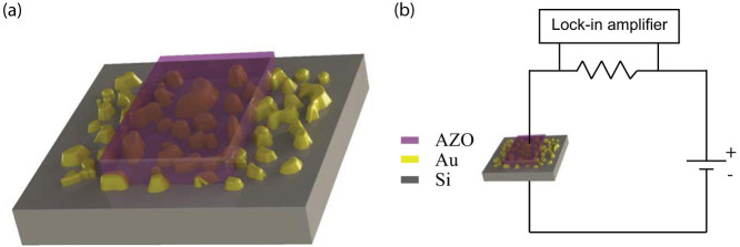
The devices have Au nanoislands on Silicon substrate, forming an Au-Si Schottky junction. An Aluminum-doped Zinc Oxide (AZO) capping layer acts as the transparent conductive oxide (TCO), creating electrical contact between the Au nanoislands and forming a heterojunction with Silicon24. A schematic view of the devices is shown in Fig. 1(a). The biasing polarity of the devices is shown in Fig. 1(b). Devices with different Au nanoisland sizes and shapes were investigated. Two types of devices were considered as references. The first reference only had the AZO capping layer on Si without any Au nanoislands (AZO reference). Without an absorbing metal layer, this reference is not expected to exhibit photoresponsivity at NIR wavelengths (the AZO layer is not expected to absorb NIR photons). The second reference had a thin continuous Au layer on Si without nanoislands and without the AZO capping layer (Au reference). Under direct illumination, surface plasmons are not excited on metal film, resulting in a very weak coupling of the incident light to the continuous metal layer. Hence, the photoresponsivity of this reference is expected to be lower than the devices with nanoislands.
Figure 1.

(a) Depiction of broad-band NIR Si Schottky photodetector. Au nanoislands are formed on n-type Si substrate by rapid thermal annealing of a thin Au film. Si substrate is used as the bottom contact; and Au nanoislands together with the AZO capping layer constitute the top contact. (b) Illustration of optoelectronic characterization setup. The photocurrent is deduced from the voltage on the series resistor. The polarity for dark current vs. voltage (I–V) measurements is also as shown in the diagram.
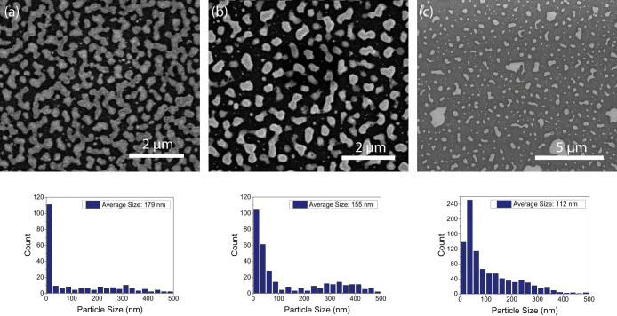
The SEM images in Fig. 2 show the effect of the annealing temperature on Au nanoisland formation. The Au layer evolves into a semi-continuous film by annealing at 300°C (Fig. 2(a)). When annealed at 450°C the Au layer forms randomly sized and randomly distributed nanoislands (Fig. 2(b)). Increasing the annealing temperature to 600°C, results in shrinkage of the nanoisland sizes (Fig. 2(c)). The particle size histogram of each SEM image also verifies the nanoparticle size reduction as the annealing temperature increases.
Figure 2. SEM image of the samples annealed at (a) 300°C, (b) 450°C, and (c) 600°C.
The sample annealed at 300°C has a semi-continuous Au film. Nanoparticles are formed on the other two samples and increasing the annealing temperature results in smaller particles. Particle size distribution histogram of each sample is plotted under the corresponding SEM image. The population of smaller particles augments with increasing annealing temperature.
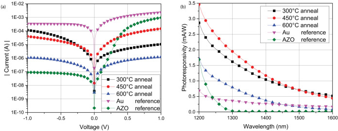
The dark I-V measurement results are plotted in Fig. 3(a). The AZO reference device, with no Au nanoislands, exhibit decent rectification and low dark current density (0.5 pA/µm2). When Au nanoislands are formed at the Silicon-AZO junction, the dark current significantly increases and the rectification property is lost. This is mainly due to the generation - recombination centers near the interface introduced by the Au nanoislands and the diffusion of Au into the Silicon and AZO layers25.
Figure 3.
(a) I–V characteristics of two reference samples and three different photodetectors with Au nanoislands. Different sized nanoislands are formed by annealing a flat Au layer at different temperatures: 300°C, 450°C, and 600°C. (b) Measured photoresponsivity spectra of the samples. AZO reference has no photoresponse for λ > 1200 nm. The other samples show sub-bandgap photoresponse by the internal photoemission process. The excitation of surface plasmons on nanoislands significantly increases the photoresponse with surface plasmon assisted hot electron generation mechanism.
Measured photoresponsivity spectra of the devices are plotted in Fig. 3(b). The AZO reference had photoresponse up to around 1200 nm wavelength, which corresponds to Silicon's band edge. Incorporation of Au to the junction allowed the absorption of sub-bandgap photons and hot carrier generation. Significant photoresponsivity enhancement was observed when the Au nanoislands were formed at the Si surface compared to the reference with flat Au layer. The photoresponsivity enhancement is due to the localized plasmon excitation at the randomly shaped nanoislands26. The device annealed at 450°C had 2 mA/W photoresponse at 1300 nm, which is the highest among all the devices investigated in this study. At longer wavelengths (λ > 1550 nm), the device annealed at 300°C had the highest photoresponse since the lower annealing temperature resulted in elongated structures, red-shifting the plasmon resonances.
Discussion
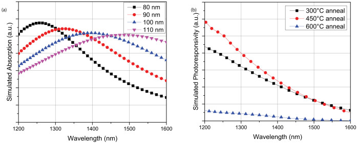
Two sets of finite difference time domain (FDTD) simulations were carried out to calculate the absorption spectra of the Au nanostructures on Silicon using Lumerical FDTD Solutions. We extracted the optical constants for AZO using J.A. Woollam Co. Inc. VASE ellipsometer and used experimental data from literature for Au and Si27,28. In the first set of simulations, we investigated the absorption spectra of identical nanoparticles periodically distributed on a Silicon substrate surrounded by AZO top layer. The periodicity was chosen to be 1000 nm and the nanoparticles with sizes 80 nm, 90 nm, 100 nm and 110 nm were simulated to observe the effect of nanoparticle size on the absorption spectrum. The absorption spectra of the nanoparticles show resonant absorption enhancement in the NIR wavelengths through the excitation of surface plasmons. The resonance wavelength makes a red-shift as the nanoparticle size increases (Fig. 4(a)). In the second set of simulations, we imported the SEM image of each fabricated sample to the FDTD software and calculated the absorption spectra of the devices. Overall response of individual plasmonic resonators with various sizes results in a broad-band absorption enhancement. Due to the increasing average particle size, the absorption spectrum is expected to red-shift as the annealing temperature decreases. The calculated absorption profiles represent the wavelength dependent generation rate of hot electrons through surface plasmon decay. In order to calculate the photoresponse of the devices, the hot electron collection rate also should be taken into account. In such a junction, hot electrons are collected by internal photoemission process.
Figure 4.
(a) Absorption spectra of 10 nm-thick single nanoparticles with different sizes calculated using FDTD simulations. (b) Calculated photoresponsivity curves of three photodetectors. Photoresponsivity values are calculated using Fowler function adjusted by simulated absorption spectra (φB ≈ 0.7 eV).
Quantum efficiency of the hot electron collection process (internal photoemission process) is given by the Fowler function25,29:
 |
where CF is the Fowler emission coefficient, hv is the energy of the incident photons and φB is the Schottky barrier height. Multiplying the Fowler function by the calculated absorption profile of the devices gives the photoresponsivity (assuming unity quantum efficiency and no other wavelength dependent factor)20. Fitting the result to the experimental responsivity data gives the Schottky barrier height to be approximately 0.7 eV, which is expected for such junctions25. The simulated photoresponsivity profile of the samples are in strong agreement with the experimental responsivity curves. This strong agreement shows that the generation and collection steps are mainly governed by surface plasmons decay and internal photoemission process, respectively.
According to the particle size histograms (Fig. 2), the sample annealed at 300°C has larger nanoislands compared to the sample annealed at 450°C. Hence, the absorption efficiency of the sample annealed at 300°C is higher in longer wavelengths and lower in shorter wavelengths. Also the crossover point (1500 nm) of the responsivity curves of these two samples predicted by the simulations agree well with measured crossover point. The experimental and simulated photoresponsivity curves are shown in Fig. 3(b) and Fig. 4(b), respectively.
Hot electron collection mechanism was utilized to achieve broad-band NIR photodetection on Si. The measured photoresponse of the devices extend up to 2000 nm wavelength. Responsivity at 1.3 µm and 1.55 µm are 2 mA/W and 600 µA/W, respectively. The results are in the same order as the peak responsivity values of the recent narrow-band plasmonically tuned photodetectors in the literature21,26,30.
The proof-of-concept demonstration was done without using any high resolution lithography or high temperature epitaxial growth technique. The planar device structure and monolithic integration capability with CMOS electronics make these devices promising for ultra-low-cost civilian NIR imaging for large volume industries such as automotive and security in addition to telecommunication industry.
Methods
(100) n-Si wafers with 2–5 Ω-cm resistivity are used as substrates. The wafers are cleaned in 4:1 H2SO4:H2O2 solution for 5 minutes, rinsed with deionized water and dipped in buffered hydrofluoric acid (BHF) solution. Au nanoislands were formed with a method similar to ref. 31. 10 nm Au layer was deposited on the samples with Gatan, Inc. Precision Etching Coating System (PECS). The samples were annealed at different temperatures for 1 minute under N2 gas flow by using rapid thermal annealing (RTA) system, resulting in randomly distributed and randomly sized Au nanoislands on Si surface. SEM images of the samples after annealing step is shown in Fig. 2. 50 nm-thick AZO is deposited on the samples using an atomic layer deposition (ALD) system (Cambridge Nanotech Inc., Savannah S100) at 250°C with trimethylaluminum (TMA), diethylzinc (DEZn) and milli-Q water (H2O) precursors. 300 µm × 600 µm active device regions are patterned with photolithography and etched with HNO3 solution. Solvent cleaning was performed prior to optical and electrical measurements.
Nanoisland size distribution measurements are done using ImageJ software. The dark I-V measurements of the devices were conducted using KEITHLEY 2401 Sourcemeter. For photoresponsivity measurements, each device was illuminated with laser light produced by a super continuum laser source (Fianium) and filtered by an acousto-optic transmission filter (AOTF - Crystal Tech.). The laser beam was aligned and focused on the devices using a custom designed optic setup. The focused beam diameter was about 50 µm and the light was normally incident on the devices. Laser light was mechanically chopped at 970 Hz and resulting photocurrent was determined by measuring the voltage on the series resistor with a lock-in amplifier (SRS830, Stanford Research Systems).
Author Contributions
M.A.N., F.B.A., B.B.T. and A.K.O. contributed equally to all parts of the research.
Acknowledgments
This work was supported by the Scientific and Technological Research Council of Turkey (TUBITAK), grant numbers 109E044, 112M004, 112E052, and 113M815. A. K. O. acknowledges support from European Union FP7 Marie Curie International Reintegration Grant (PIOS, Grant # PIRG04-GA-2008-239444). A. K. O. acknowledges support from the Turkish Academy of Sciences Distinguished Young Scientist Award (TUBA GEBIP). F. B. A. acknowledges TUBITAK-BIDEB national PhD Fellowship.
References
- Soole J. B. & Schumacher H. InGaAs metal-semiconductor-metal photodetectors for long wavelength optical communications. IEEE J. Quantum Electron. 27, 737–752 (1991). [Google Scholar]
- Campbell J. C. Recent advances in telecommunications avalanche photodiodes. Lightwave Technol. 25, 109–121 (2007). [Google Scholar]
- Blanco M. & Villarroya I. NIR spectroscopy: a rapid-response analytical tool. TrAC, Trends Anal. Chem. 21, 240–250 (2002). [Google Scholar]
- Osborne B. G., Fearn T. & Hindle P. H. Practical NIR Spectroscopy with Applications in Food and Beverage Analysis (Longman scientific and technical, 1993). [Google Scholar]
- Hansen M. P. & Malchow D. S. Overview of SWIR detectors, cameras, and applications. In SPIE Defense and Security Symposium. SPIE Defense and Security Symposium. International Society for Optics and Photonics. 69390I–69390I (2008). [Google Scholar]
- Brouckaert J., Roelkens G., Van Thourhout D. & Baets R. Thin-film III–V photodetectors integrated on silicon-on-insulator photonic ICs. Lightwave Technol. 25, 1053–1060 (2007). [Google Scholar]
- Herrscher M. et al. Epitaxial liftoff InGaAs/InP MSM photodetectors on Si. Electron. Lett. 31, 1383–1384 (1995). [Google Scholar]
- WALDEN R. H. A review of recent progress in InP-based optoelectronic integrated circuit receiver front-ends. Int. J. High Speed Electron. Syst. 9, 631–642 (1998). [Google Scholar]
- Okyay A. K. et al. High-efficiency metal-semiconductor-metal photodetectors on heteroepitaxially grown Ge on Si. Opt. Lett. 31, 2565–2567 (2006). [DOI] [PubMed] [Google Scholar]
- Fidaner O. et al. Ge–SiGe quantum-well waveguide photodetectors on silicon for the near-infrared. IEEE Photonics Technol. Lett. 19, 1631–1633 (2007). [Google Scholar]
- Okyay A. K. et al. SiGe optoelectronic metal-oxide semiconductor field-effect transistor. Opt. Lett. 32, 2022–2024 (2007). [DOI] [PubMed] [Google Scholar]
- Tang L. et al. Nanometre-scale germanium photodetector enhanced by a near-infrared dipole antenna. Nat. Photonics. 2, 226–229 (2008). [Google Scholar]
- Yu H. Y. et al. High-efficiency pin photodetectors on selective-area-grown Ge for monolithic integration. IEEE Electron Device Lett. 30, 1161–1163 (2009). [Google Scholar]
- Onaran E. et al. Silicon-Germanium multi-quantum well photodetectors in the near infrared. Opt. Express, 20, 7608–7615 (2012). [DOI] [PubMed] [Google Scholar]
- Yu H. Y., Park J. H., Okyay A. K. & Saraswat K. C. Selective-Area High-Quality Germanium Growth for Monolithic Integrated Optoelectronics. IEEE Electron Device Lett. 33, 579–581 (2012). [Google Scholar]
- Shepherd Jr F. D., Yang A. C. & Taylor R. W. A 1 to 2 µm silicon avalanche photodiode. Proc. IEEE. 58, 1160–1162 (1970). [Google Scholar]
- Endriz J. G. & Spicer W. E. Surface-plasmon-one-electron decay and its observation in photoemission. Phys. Rev. Lett. 24, 64 (1970). [Google Scholar]
- Akbari A., Tait R. N. & Berini P. Surface plasmon waveguide Schottky detector. Opt. Express. 18, 8505–8514 (2010). [DOI] [PubMed] [Google Scholar]
- Akbari A. & Berini P. Schottky contact surface-plasmon detector integrated with an asymmetric metal stripe waveguide. Appl. Phys. Lett. 95, 021104 (2009). [Google Scholar]
- Knight M. W., Sobhani H., Nordlander P. & Halas N. J. Photodetection with active optical antennas. Science. 332, 702–704 (2011). [DOI] [PubMed] [Google Scholar]
- Sobhani A. et al. Narrowband photodetection in the near-infrared with a plasmon-induced hot electron device. Nat. Commun. 4, 1643 (2013). [DOI] [PubMed] [Google Scholar]
- Wang F. & Melosh N. A. Plasmonic energy collection through hot carrier extraction. Nano Lett. 11, 5426–5430 (2011). [DOI] [PubMed] [Google Scholar]
- Atar F. B. et al. Plasmonically enhanced hot electron based photovoltaic device. Opt. Express. 21, 7196–7201 (2013). [DOI] [PubMed] [Google Scholar]
- Ismail R. A., Al-Naimi A. & Al-Ani A. A. Studies on fabrication and characterization of a high-performance Al-doped ZnO/n-Si (1 1 1) heterojunction photodetector. Semicond. Sci. Technol. 23, 075030 (2008). [Google Scholar]
- Sze S. M. & Ng K. K. Physics of Semiconductor Devices (John Wiley & Sons, 2006). [Google Scholar]
- Li W. & Valentine J. G. Metamaterial Perfect Absorber Based Hot Electron Photodetection. Nano lett. (2014). [DOI] [PubMed] [Google Scholar]
- Johnson P. B. & Christy R. W. Optical constants of the noble metals. Phys. Rev. B. 6, 4370 (1972). [Google Scholar]
- Palik E. D. Handbook of Optical Constants of Solids (Academic press, 1998). [Google Scholar]
- Fowler R. H. The analysis of photoelectric sensitivity curves for clean metals at various temperatures. Phys. Rev. 38, 45 (1931). [Google Scholar]
- Lin K. T., Chen H. L., Lai Y. S. & Yu C. C. Silicon-based broadband antenna for high responsivity and polarization-insensitive photodetection at telecommunication wavelengths. Nat. Commun. 5 (2014). [DOI] [PubMed] [Google Scholar]
- Lee K. C., Lin S. J., Lin C. H., Tsai C. S. & Lu Y. J. Size effect of Ag nanoparticles on surface plasmon resonance. Surf. Coat. Technol. 202, 5339–5342 (2008). [Google Scholar]


