Abstract
We report on the use of nucleic acid bases (NBs) in organic light emitting diodes (OLEDs). NBs are small molecules that are the basic building blocks of the larger DNA polymer. NBs readily thermally evaporate and integrate well into the vacuum deposited OLED fabrication. Adenine (A) and thymine (T) were deposited as electron-blocking/hole-transport layers (EBL/HTL) that resulted in increases in performance over the reference OLED containing the standard EBL material NPB. A-based OLEDs reached a peak current efficiency and luminance performance of 48 cd/A and 93,000 cd/m2, respectively, while T-based OLEDs had a maximum of 76 cd/A and 132,000 cd/m2. By comparison, the reference OLED yielded 37 cd/A and 113,000 cd/m2. The enhanced performance of T-based devices is attributed to a combination of energy levels and structured surface morphology that causes more efficient and controlled hole current transport to the emitting layer.
Natural electronics is an area of research that searches for naturally occurring or naturally derived biomolecules to replace traditional synthesized materials in solid-state organic electronics1. Biomolecules often have natural electrical and optical properties that are fine-tuned to improve device performance2,3,4,5. While the main goal is to enhance performance, naturally occurring biomolecules also support renewable and environmentally responsible electronics, with potentially a concomitant reduction in cost6. The deoxyribose nucleic acid (DNA) polymer has been a frequent natural material integrated in electronic devices. DNA has been used in organic light-emitting diodes (OLEDs)4,5,7,8,9,10,11,12,13,14 yielding significant increases in efficiency and luminance. Other thin film organic devices15,16,17,18,19,20,21 have also benefited from the natural biopolymer. However, DNA requires extensive processing and wet fabrication to form thin films22.
In this study we expand the “toolbox” of natural electronics by reporting on the use of thymine and adenine, two nucleic acid bases or nucleobases (NBs), to improve OLED performance. NBs have been incorporated into OFETs3,23,24,25 but DNA still remains one of the only bio-based materials for OLEDs, which confines the design structures of devices to the inherent optoelectronic properties of DNA. Thymine (T) and adenine (A) are two of the four nitrogenous bases that are constituents of the larger DNA polymer. T belongs to the pyrimidine family with a single heterocyclic ring, while A is from the purine group and consists of two fused rings. T and A bases form a hydrogen-bonded base pair in the DNA double helix. NBs are available in powder form and require no surfactant modification or wet processing, unlike DNA, for thin film formation. They readily form thin films by thermal evaporation and integrate well into standard dry fabrication for OLEDs. In this study, T was incorporated as an electron blocking layer/hole transport layer (EBL/HTL) in a typical green phosphorescent OLED. T-based OLEDs achieved a current efficiency of 76 cd/A, which represents a > 200% increase in efficiency over the reference device (~37 cd/A) that had a standard EBL/HTL material. The A-based device also outperformed the reference device with a maximum current efficiency of 48 cd/A and displayed reduced roll-off for efficiency at high voltages.
Methods
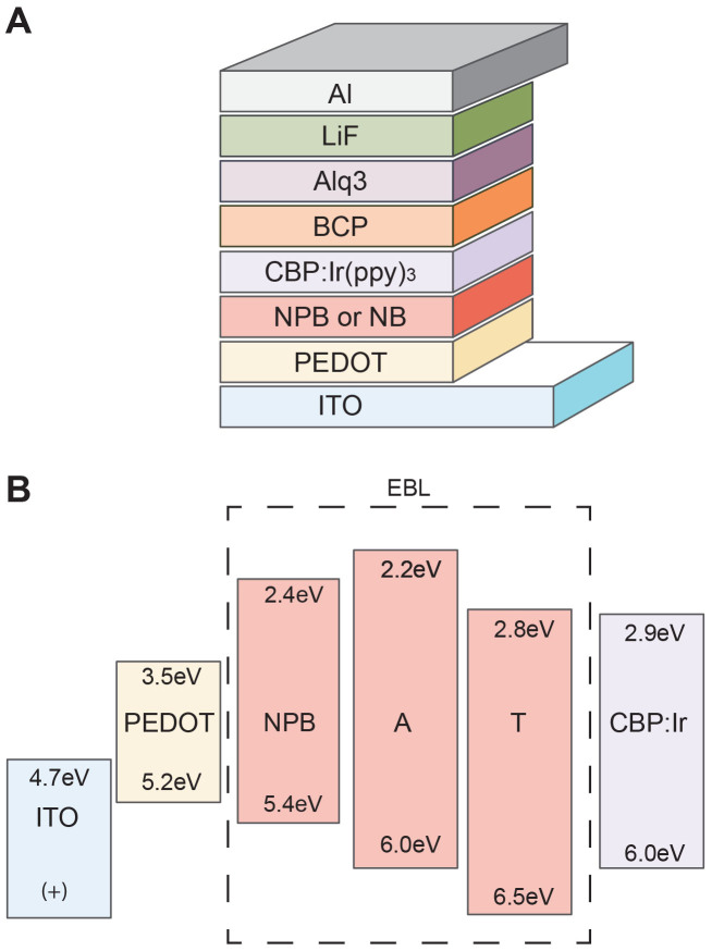
OLEDs were fabricated on glass/ITO substrates that were rinsed in organic solvents followed by exposure to oxygen plasma for 10 min. After cleaning, filtered PEDOT:PSS [poly(3,4-ethylenedioxythiophene) doped with poly(4-styrenesulfonate)] (Clevios P VP AI 4083) was spin-coated onto the glass/ITO substrates and baked at 120°C for 15 min before depositing organic and metal (electrode) layers in a molecular beam deposition (MBD) system (SVT Assoc., St. Paul, MN). The NB materials (Sigma Aldrich) and the other organic materials (Luminescence Technology Corp. Taiwan) were used as received. Figure 1a shows the configuration of the reference and NB OLEDs (with A and T). Three device types were fabricated consisting of the following structure: ITO [90 nm]/PEDOT:PSS[40 nm]/X[10 nm]/CBP:Ir(ppy)3 (10wt%)[30 nm]/BCP[12 nm]/Alq3[25 nm]/LiF[1 nm]/Al[40 nm]. X was the EBL/HTL layer for the three devices: NPB (as a reference device), T (to represent the pyrimidines), or A (to represent the purines). T and A were thermally evaporated at ~160–180°C. The film thickness was measured by a quartz crystal monitor during deposition and subsequently verified by ellipsometry.
Figure 1. The device configuration of the OLED.
(A) The EBL contains NPB (reference device) or a nucleobase (A or T). (B) Molecular orbital energy levels for the EBL materials and the levels of adjacent materials.
Results and Discussion
Figure 1b presents a comparison of estimated highest occupied molecular orbital (HOMO) and lowest unoccupied molecular orbital (LUMO) energy levels for the EBL/HTL materials (in the dashed box) adjacent to the PEDOT:PSS (hole injection) layer and the CBP:Ir(ppy)3 (emitting) layer. The HOMO/LUMO levels shown are orbital computations for all of the NBs reported by Faber et al.26. A has a HOMO level of 6.0 eV that matches the adjacent host for the emitting layer (CBP) and is higher than that of the NPB. T has a HOMO level that is slightly higher at 6.5 eV. The bases have a wide molecular orbital gap of ~3.7–3.8 eV placing the LUMO at 2.2 and 2.8 eV for A and T, respectively. Lee et al.27 has reported energy levels obtained by ultraviolet photoemission spectroscopy (UPS) measurements on A and T thin films that indicated larger HOMO (6.6 eV and 7.0 eV for A and T, respectively), and LUMO energy levels (2.5 and 2.9 eV for A and T, respectively), resulting in an equal gap of 4.1 eV.
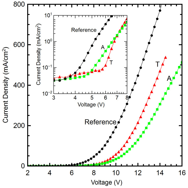
OLED current-voltage (I–V) characterization was performed with an HP-6634B DC power source at 0.25 V intervals and the luminance was measured using a Konica-Minolta CS-200 luminance meter. I–V characteristics are presented in Figure 2. The turn-on voltage (defined here when luminance was detectable by the meter) for the reference device was 3.75 V, while the A device turned on at 4.5 V. The T device had a larger turn-on voltage of 5.5 V. As shown in the Figure 2 insert, the T device had a steeper slope between 6 and 7 V, beyond which its current surpassed the A device while remaining below that of the reference device.
Figure 2. Current density versus voltage of the devices being compared.
T device shows larger current density over the A devices but the current remains lower than the reference as the voltage increases (All EBL thicknesses are 10 nm). INSET - Detailed view of the turn-on voltage region.
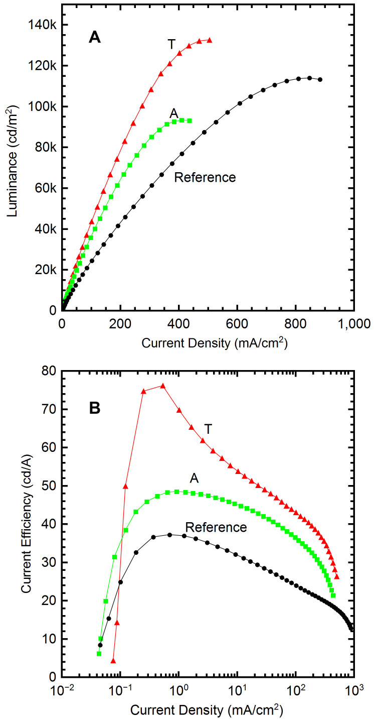
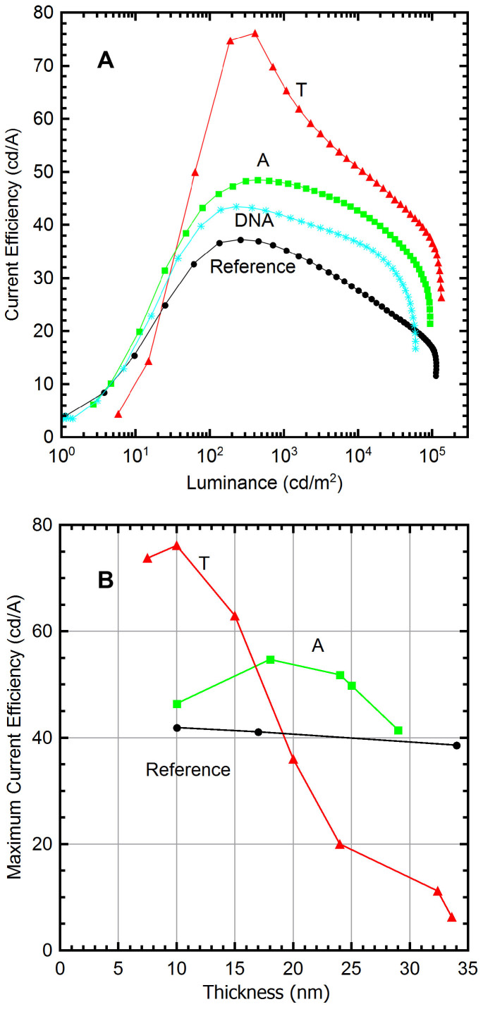
The device luminance as a function of current density is shown in Figure 3(a) for all three devices. T and A devices had a much steeper slope than the reference resulting in higher luminance at lower current. The T device achieved a maximum luminance of 132,000 cd/m2; the A device reached 93,000 cd/m2; the reference device maximum was 113,000 cd/m2. Figure 3(b) presents the current efficiency trend versus current density. The peak efficiency occurs for all devices between ~0.2–0.5 mA/cm2, with the T device exhibiting the largest performance. A similar efficiency plot also is given in Figure 4(a) with respect to luminance. The T device reached a peak current efficiency of 76 cd/A at 400 cd/m2. The efficiency was 51 cd/A at 10,000 cd/m2 and 36 cd/A at 100,000 cd/m2. At the maximum luminance of 132,000 cd/m2 (obtained at 14 V) the current efficiency for the T device was 26 cd/A. By comparison, the reference device had a maximum efficiency of only 37 cd/A (at 260 cd/m2), less than half that of the T device at the same luminance. The A OLED had a maximum current efficiency of ~48 cd/A at 300 cd/m2, also outperforming the reference. The A device current efficiency experienced a reduced roll-off effect, decreasing to only 42cd/A at 10,000 cd/m2.
Figure 3. OLED Characteristics.
(A) Luminance as a function of current density showing with the NB devices with a larger luminance than the reference device, over the entire current density range. (B) Current efficiency vs. current density, with the T device reaching peak efficiency of 76 cd/A at ~0.2–0.5 mA/cm2.
Figure 4. Optimized EBL thickness of each device.
(A) Current efficiency vs. luminance, with the T device reaching a peak efficiency of 76 cd/A at ~200–400 cd/m2. The NBs are also preferred over the DNA-CTMA at 0.25wt% (~10 nm) for efficiency and luminance performance. (B) T layer produced peak efficiency at 10 nm, while A had optimum thickness of ~17 nm. Efficiency of reference OLED not affected by NBP layer thickness (10–35 nm).
To compare the results to DNA bio-OLED performance, a device was fabricated with DNA-CTMA as the EBL layer in the OLED structure for this work (Figure 1). The surfactant complex and the DNA (200 kDa) thin film fabrication followed previously documented procedures28, dissolving DNA-CTMA in butanol at 0.25wt% and spin coating for the EBL (~10 nm). DNA-CTMA OLED obtained a peak current efficiency of 43 cd/A at 230 cd/m2, as shown in Figure 4, with a maximum luminance of 62,000 cd/m2. The results show that the DNA-based OLED surpasses the reference device in current efficiency over nearly the entire luminance range. The A and T-based OLEDs, however, in addition to the advantage of their simpler fabrication process, exceed the DNA-based OLED in current efficiency and maximum luminance.
The thickness of the EBL was varied for each of the three device configurations. Using the maximum current efficiency as the key performance measure, the optimum thickness for the T layer devices was found to be ~10 nm, producing the greatest performance increase over the reference, as shown in Figure 4(b). Increasing the T layer thickness beyond 10 nm caused a significant loss of performance due to its large HOMO level, which effectively halts hole transport. Decreasing the T layer thickness to less than 10 nm also decreased performance, as a surplus of holes can be injected creating a charge imbalance and a reduction in current emission efficiency. The A device showed a similar trend, with a less pronounced optimum thickness at ~17 nm.
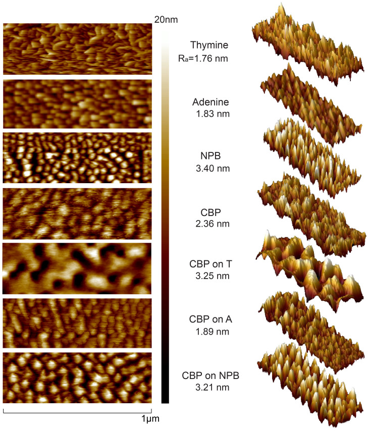
Atomic force microscopy (AFM) studies were performed to examine the surface morphology of the NB films and subsequent layers. First, AFM was done on the T, A, NPB, and CBP (the host material of the emitting layer) thin films that were deposited onto silicon substrates with the same parameters that were used during the OLED fabrication (10 nm for the EBL and 30 nm for CBP). Next, CBP was deposited on top of T, A, and NPB films to a thickness of 30 nm and AFM was performed on top of the CBP layer to observe how the emitting layer forms on top of each under-layer. Figure 5 shows AFM scans of each film. The horizontal scan length was 1 μm and the vertical scale was 20 nm. T and A had similar roughness (1.76 and 1.83 nm, respectively), but the T AFM scan revealed a range of random crystallites in both surface periodicity and height distribution. The A AFM scan indicated more uniform distribution of crystallites with regard to both periodicity and height distribution. It is noteworthy to compare with reports that T crystallites grow into large columnar-like structures, while the A has lower height distribution29. The NPB layer exhibited relatively large roughness (3.4 nm) with similar periodicity and grain size as A. The CBP film deposited on A retained a similar roughness (1.9 nm) and grain size to that of CBP on Si (2.4 nm). CBP on NBP (3.2 nm) resembled the NBP on Si roughness (3.4 nm) but with the grain size of CBP on Si. While in the cases of CBP on A and on NPB, the roughness and morphology of the CBP resembled the layer it was deposited on, the case of the CBP layer on T appears to differ significantly. The CBP on T had much higher roughness (3.25 nm) than T on Si (1.75 nm) and its morphology is significantly changed, exhibiting relatively deep (20+ nm) and wide (50–100 nm) craters dispersed throughout the layer.
Figure 5. AFM of thin films.
AFM scan of each EBL deposited to 10 nm and CBP deposited on silicon to 30 nm. Also shown are AFM scans on CBP deposited on top of each EBL film. Scan length is 1 μm; surface roughness is provided for each scan along with 3D views for each layer.
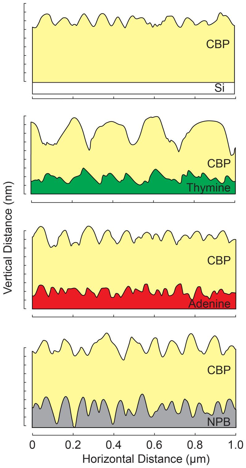
Figure 6 illustrates the morphology of the CBP layer on several under-layers, based on a representative horizontal line scan sampled from the corresponding AFM image. The CBP scans are stacked on top of each corresponding EBL in order to observe the effect that the EBL layer morphology has on the growth of the CBP. It is clear that the CBP on T is significantly different from the other cases. There may be several possible explanations for the linkage between the large craters observed in the CBP layer and higher performance of the T-based OLED. One possible mechanism is related to enhancement of light extraction due to formation of crater-based microcavities that disperse the emitted light and increase its outcoupling efficiency. A second possible explanation has to do with the significant variation in the CBP profile. For small values of T, the deeper CBP craters may provide for efficient injection from the T layer and recombination in the CBP emitting layer. Interestingly, the T-based OLED results resemble the charge trapping effect of nanoparticles in the PEDOT layer of a phosphorescent OLED30 that enhances the efficiency by controlling the charge balance. As the T layer thickness is increased, the effect of its properties (higher resistance than NPB) dominates over the CBP morphology and the current efficiency drops dramatically, as seen in Fig. 4A. It is important to also note that the morphological similarities between CBP on A and on NPB are somewhat mirrored in their corresponding dependence of current efficiency on EBL thickness (Fig. 4B).
Figure 6. 2D AFM plots.
A line scan of each AFM result plotted on vertical/horizontal axes. The AFM results for the CBP are shown for deposition on Si and on each EBL. Each CBP line scan was paired to its respective layer it was grown on in order to elucidate how each EBL affects the growth of the emitting layer.
In summary, the A and T nucleobases have been shown to lead to high photoemission efficiency OLEDs. Thin film NBs produce performance enhancement due to the effect of their large HOMO energy level that creates a more balanced electron/hole ratio in the device. Additionally, the unique surface morphology of T combined with that of the emitting layer (CBP) provides high efficiency regions for hole transport between PEDOT:PSS and the emitting layer. This preliminary study of NBs in OLEDs indicate that their charge transport properties, relative low cost, minimal pre-fabrication processing, and natural origin could open new opportunities in future natural electronics devices.
Author Contributions
E.F.G. performed all device and AFM experiments. E.F.G. and A.J.S. wrote the manuscript and prepared all figures. V.V. and J.G.G. participated in helpful discussions about the data and reviewed the manuscript.
References
- Irimia-Vladu M. “Green” electronics: biodegradable and biocompatible materials and devices for sustainable future. Chem. Soc. Rev. 43, 588–610, 10.1039/c3cs60235d (2014). [DOI] [PubMed] [Google Scholar]
- Irimia-Vladu M., Sariciftci N. S. & Bauer S. Exotic materials for bio-organic electronics. J. Mater. Chem. 21, 1350–1361, 10.1039/c0jm02444a (2011). [Google Scholar]
- Lee J. et al. DNA-base guanine as hydrogen getter and charge trapping layer embedded in oxide dielectrics for inorganic and organic field-effect transistors. ACS Appl. Mater. Interfaces 6, 4965–4973, 10.1021/am405998d (2014). [DOI] [PubMed] [Google Scholar]
- Hagen J. A., Li W., Steckl A. J. & Grote J. G. Enhanced emission efficiency in organic light-emitting diodes using deoxyribonucleic acid complex as an electron blocking layer. Appl. Phys. Lett. 88, 171109, 10.1063/1.2197973 (2006). [Google Scholar]
- Steckl A. J., Spaeth H., You H., Gomez E. & Grote J. DNA as an optical material. Opt. Photon. News 22, 34–39, 10.1364/OPN.22.7.000034 (2011). [Google Scholar]
- Mühl S. & Beyer B. Bio-organic electronics–overview and prospects for the future. Electron. 3, 444–461 (2014). [Google Scholar]
- Steckl A. J. DNA - a new material for photonics? Nature Photon. 1, 3 10.1038/nphoton.2006.56 (2007). [Google Scholar]
- Sun Q. et al. Highly efficient quantum-dot light-emitting diodes with DNA-CTMA as a combined hole-transporting and electron-blocking layer. ACS Nano 3, 737–743, 10.1021/nn8009079 (2009). [DOI] [PubMed] [Google Scholar]
- Nakamura K., Ishikawa T., Nishioka D., Ushikubo T. & Kobayashi N. Color-tunable multilayer organic light emitting diode composed of DNA complex and tris(8-hydroxyquinolinato)aluminum. Appl. Phys. Lett. 97, 193301, 10.1063/1.3512861 (2010). [Google Scholar]
- Chen I. C., Chiu Y.-W., Fruk L. & Hung Y.-C. Enhanced light emission from blue organic light-emitting devices with DNA biopolymer. Paper presented at Proc IQEC/CLEO Pacific Rim 2011, Sydney Australia. 10.1109/IQEC-CLEO.2011.6193872 (2011).
- Sun Q., Chang D. W., Dai L., Grote J. & Naik R. Multilayer white polymer light-emitting diodes with deoxyribonucleic acid-cetyltrimetylammonium complex as a hole-transporting/electron-blocking layer. Appl. Phys. Lett. 92, 251108, 10.1063/1.2948864 (2008). [Google Scholar]
- Madhwal D. et al. Increased luminance of MEH-PPV and PFO based PLEDs by using salmon DNA as an electron blocking layer. J. of Lumin. 130, 331–333, 10.1016/j.jlumin.2009.09.012 (2010). [Google Scholar]
- Gupta R. B., Nagpal S., Arora S., Bhatnagar P. K. & Mathur P. C. Ultraviolet electroluminescence from zinc oxide nanorods/deoxyribonucleic acid hybrid bio light-emitting diode. J. of Nanophoton. 5, 059505, 10.1117/1.3618630 (2011). [Google Scholar]
- Zalar P. et al. DNA electron injection interlayers for polymer light-emitting diodes. J. Am. Chem. Soc. 133, 11010–11013, 10.1021/ja201868d (2011). [DOI] [PubMed] [Google Scholar]
- Singh T., Sariciftci N. & Grote J. Bio-Organic Optoelectronic Devices Using DNA. In:: Organic Electronics Vol 233 Advances in Polymer Science. Grasser, T., Meller, G. & Li, L. (eds.) Ch. 6, 73–112 (Springer Berlin Heidelberg, 2010). [Google Scholar]
- Heckman E. M., Grote J. G., Hopkins F. K. & Yaney P. P. Performance of an electro-optic waveguide modulator fabricated using a deoxyribonucleic-acid-based biopolymer. Appl. Phys. Lett. 89, 181116, 10.1063/1.2378400 (2006). [Google Scholar]
- Yu Z. et al. Photoluminescence and lasing from deoxyribonucleic acid (DNA) thin films doped with sulforhodamine. Appl. Opt. 46, 1507–1513 (2007). [DOI] [PubMed] [Google Scholar]
- Kim Y. S. et al. High-mobility bio-organic field effect transistors with photoreactive DNAs as gate insulators. Appl. Phys. Lett. 96, 103307, 10.1063/1.3299022 (2010). [Google Scholar]
- Zhang Y. et al. DNA interlayers enhance charge injection in organic field-effect transistors. Adv. Mater. 24, 4255–4260, 10.1002/adma.201201248 (2012). [DOI] [PubMed] [Google Scholar]
- Ouchen F. et al. Deoxyribonucleic acid-ceramic hybrid dielectrics for potential application as gate insulators in organic field effect transistors. Appl. Phys. Lett. 103, 113701, 10.1063/1.4821019 (2013). [Google Scholar]
- Joyce D. M. et al. Deoxyribonucleic acid-based hybrid thin films for potential application as high energy density capacitors. J. Appl. Phys. 115, 114108, 10.1063/1.4868339 (2014). [Google Scholar]
- Heckman E. M., Hagen J. A., Yaney P. P., Grote J. G. & Hopkins F. K. Processing techniques for deoxyribonucleic acid: biopolymer for photonics applications. Appl. Phys. Lett. 87, 211115, 10.1063/1.2135205 (2005). [Google Scholar]
- Irimia-Vladu M. et al. Biocompatible and biodegradable materials for organic field-effect transistors. Adv. Funct. Mater. 20, 4069–4076, 10.1002/adfm.201001031 (2010). [Google Scholar]
- Maruccio G. et al. Field effect transistor based on a modified DNA base. Nano Lett. 3, 479–483, 10.1021/nl034046c (2003). [Google Scholar]
- Shi W., Yu J., Huang W. & Zheng Y. Performance improvement of a pentacene organic field-effect transistor through a DNA interlayer. J. Phys. D: Appl. Phys. 47, 205402, 10.1088/0022-3727/47/20/205402 (2014). [Google Scholar]
- Faber C., Attaccalite C., Olevano V., Runge E. & Blase X. First-principles GW calculations for DNA and RNA nucleobases. Phys. Rev. B 83, 115123, 10.1103/PhysRevB.83.115123 (2011). [Google Scholar]
- Lee Y., Lee H., Park S. & Yi Y. Energy level alignment at the interfaces between typical electrodes and nucleobases: Al/adenine/indium-tin-oxide and Al/thymine/indium-tin-oxide. Appl. Phys. Lett. 101, 233305, 10.1063/1.4769438 (2012). [Google Scholar]
- Gomez E. F., Spaeth H. D., Steckl A. J. & Grote J. G., Fabrication of natural DNA-containing organic light emitting diodes. Paper presented at Proc. SPIE 8103, Nanobiosystems: Processing, Characterization, and Applications IV San Diego, California, USA, 10.1117/12.899397 (2011, September 15). [Google Scholar]
- Irimia-Vladu M. et al. Environmentally sustainable organic field effect transistors. Org. Electron. 11, 1974-1990, 10.1016/j.orgel.2010.09.007 (2010). [Google Scholar]
- Ji W. Wang J. Zeng Q. Su Z. & Sun Z. Highly efficient organic light-emitting devices by introducing traps in the hole-injection layer. RSC Adv. 3, 14616-14621, 10.1039/C3RA42320D (2013). [Google Scholar]


