Abstract
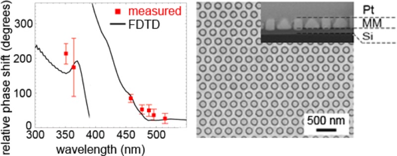
We report the experimental realization of an optical metamaterial composed of a hexagonal array of coaxial plasmonic metal/insulator/metal waveguides that shows strong polarization-independent optical mode index dispersion in the ultraviolet/blue. The metamaterial is composed of silicon coaxes with a well-defined diameter in the range of 150–168 nm with extremely thin sidewalls (13–15 nm), embedded in a silver film, fabricated using a combination of electron beam lithography, physical vapor deposition, reactive ion etching, and focused ion beam polishing. Using a Mach–Zehnder interferometer the phase advance is measured on several metamaterial samples with different dimensions in the UV/visible part of the spectrum. For all geometries the spectral features as well as the geometry dependence of the data correspond well with numerical finite-difference time domain simulations and the calculated waveguide dispersion diagram, showing a negative mode index between 440 and 500 nm.
Keywords: Plasmonics, metamaterial, negative index, optical interferometry, nanofabrication
Optical metamaterials are materials built from subwavelength-scale dielectric, semiconductor, and/or metal building blocks that, together, lead to effective optical properties that do not exist in natural materials. One important class of optical metamaterials is composed of noble-metal resonant structures with a magneto-electric response (e.g., split ring resonators), embedded in a dielectric material. The interplay between the magnetic and electric resonances can lead to an effective refractive index that is negative,1 implying that the phase velocity of light is negative and that light shows negative refraction at an interface. Negative refraction using such geometries was first experimentally demonstrated in the microwave spectral range2 and more recently in the near-infrared.3,4 However, the realization of negative-index metamaterials in the ultraviolet and visible spectral range using this concept has proven impossible because it requires scaling of the resonator geometry5 to dimensions that cannot reliably be reached using electron beam lithography techniques. Furthermore, these designs relying on localized resonances strongly absorb light6 and only work for a very narrow bandwidth. Yet, the realization of a UV/visible metamaterial with a refractive index designed by geometry is of great interest because it may enable the realization of a polarization-independent flat lens7 and would find applications in novel (micro)optical components, superradiant light sources, transformation optics, and optical cloaking,8,9 to mention a few examples.10
To circumvent the fundamental fabrication and Ohmic dissipation problems associated with nanoresonator metamaterials operating in the UV/visible, we have proposed an alternative metamaterials architecture11 in which the metamaterial is built up from arrays of metal/insulator/metal waveguides that support surface plasmon polaritons (SPP). The dispersion of these coupled plasmonic waveguides is tunable by the dimensions of the metamaterial, and as shown before, two-dimensional SPP waveguides can show a negative mode index, over a relatively large wavelength range, for the asymmetric in-plane plasmonic waveguide mode.12 As we have subsequently shown, a specially designed three-dimensional array of SPP waveguides can act as a three-dimensional metamaterial with an isotropic negative index for the fundamental harmonic, due to out-of-plane coupling between the parallel planar metal/insulator/metal waveguides.11,13 Negative refraction of energy has recently been demonstrated experimentally in such structures.14 However, this geometry only works for TM-polarized light. To create a polarization-independent metamaterial, we have proposed that SPP waveguides can be “rolled-up” to form an array of coupled coaxial plasmonic waveguides (see Figure 1).15 This geometry is composed of Si cylinders with a wall thickness of 10–20 nm, which are embedded in a metal film. The asymmetric SPP mode that results from coupling of SPPs across the Si cylinders is tuned by geometry to have a negative mode index. Coupling between the cylinders will then lead to a negative index out of the plane of the waveguides, which is the result of the key fact that the asymmetric modes are coupled.11 As we have shown by numerical simulations,15 the propagation of light in these rolled-up structures is still described by the coupling of plasmonic waveguides with an effective mode index that is negative, but because of the symmetry the effective index is nearly independent of angle and polarization. This coaxial plasmonic waveguide (CPW) design thus provides another advantage over the split-ring geometry for which the index depends on the polarization of the incoming light. Moreover, the loss figure-of-merit of the CPW design, describing the propagation length in the material relative to the free-space wavelength, is higher than that for the split-ring design (FOM < 3 for split ring resonators,6 compared to a FOM < 18 for the CPW design16). The figure of merit for the metamaterial discussed in this letter is shown in Figure 5b. Furthermore, the CPW isotropic metamaterial design can be tuned to possess a broad variety of refractive indices n, including very large negative or positive values of n including the special cases of n = 0 and n = −1.
Figure 1.
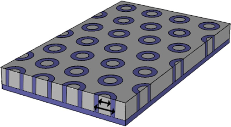
Coaxial plasmonic metamaterial geometry. Coaxial plasmonic hexagonal metal (gray)/insulator (purple)/metal waveguide array. The smallest arrow defines the inner diameter (da), the largest arrow the outer diameter (db). The coaxial Si wall thickness is defined as (db – da)/2.
Figure 5.

Single-coax SPP dispersion. (a) Calculated SPP dispersion diagram of an infinitely long, single Si cylinder embedded in silver, with outer diameter 168 nm, and cylinder wall thickness 15 nm (as in sample 1). Both the real (solid line) and imaginary (dotted line) parts of the positive (red) and negative (blue) index mode are plotted. (b) Figure-of-merit (FOM) of the positive (red) and negative (blue) index mode. The FOM is defined as |n′/n″|, with n′ and n″ the real and imaginary part of the mode index shown in panel a, respectively. The black dots show the FOM calculated from the refractive index extracted from FDTD simulations (Table 2). (c) FDTD simulation of the transmission spectrum of the experimental metamaterial sample 1 (red), the 49 nm thick silicon membrane only (black), and the 91 nm thick metamaterial only (blue).
While the CPW design has thus been theoretically and numerically predicted to show the desired negative-index behavior, its experimental realization so far has remained elusive. Here, we present the experimental demonstration of a hexagonal Ag/Si CPW geometry fabricated using a combination of electron-beam lithography (EBL), reactive ion etching (RIE), metal infiltration using electron beam physical vapor deposition (EBPVD), and focused ion beam (FIB) polishing. We perform optical interferometry to measure the phase evolution of light inside the coaxial metamaterial in the ultraviolet/blue/green spectral range (λ = 351–515 nm). The measured phase is highly dispersive and in agreement with numerical simulations and the calculated waveguide mode dispersion diagram, showing a negative mode index for λ = 440–500 nm.
The fabrication of the hexagonal coaxial metamaterial (see Figure 2a) starts with patterning a 1 μm thick Si(100) membrane with 100 keV EBL, using the high-resolution resist hydrogen silsesquioxane (HSQ). After development in a 5% tetramethylammonium hydroxide (TMAH) solution at 50 °C we obtain hollow pillars of HSQ with a height up to 250 nm and wall thickness as small as 7 nm. Using these rings as etch mask, the coaxial structure is transferred into the Si membrane with anisotropic RIE (SF6/CHF3). After an HF dip to remove the remains of the resist we infill the structures with Ag, using a newly developed EBPVD method in which the sample is mounted at the center of a rotation stage, with the sample normal to the silver vapor and tilted 60° with respect to an Ar+ ion beam. The sample is rotated with 30 rpm during the entire process. After every 15 nm of metal depositing we shave off the excess of Ag growing on top of the Si coaxes with a 2 mA 300 eV Ar+ ion beam for 200 s. During the ion shaving the evaporation is stopped. A sketch of the evaporation process is shown in Supplementary Figure S1. This new technique leads to fully conformal infiltration of Ag, minimizing shadowing effects of Ag deposited on top of the Si cylinders. The sample surface is then polished and made optically accessible with 30 keV Ga+ FIB milling under grazing incidence. Finally, a RIE back etch is performed to reduce the thickness of the supporting Si layer. SEM images of the metamaterial after different steps of the fabrication process are shown in Figure 2b. The final metamaterial samples, with dimensions of 20 × 20 μm, consist of Si rings with a well-defined diameter in the range of 150–168 nm and a wall thickness of <15 nm, embedded in Ag (Figure 2b-4). Table 1 lists the dimensions of each of the different CPW metamaterials that was made, measured using SEM. Both top-view SEM images and cross sections using focused-ion beam milling were made. The outer diameter of the Si cylinders is varied from 150 to 168 nm, while the pitch ranges from 200 to 300 nm in steps of 50 nm. The key feature, and the experimentally most challenging one to realize, is the Si cylinder wall thickness; it ranges from 13 to 15 nm. It is this small thickness that leads to strong SPP coupling across the wall thickness of the Si cylinder and hence a negative mode index for SPPs propagating along the cylinders.
Figure 2.
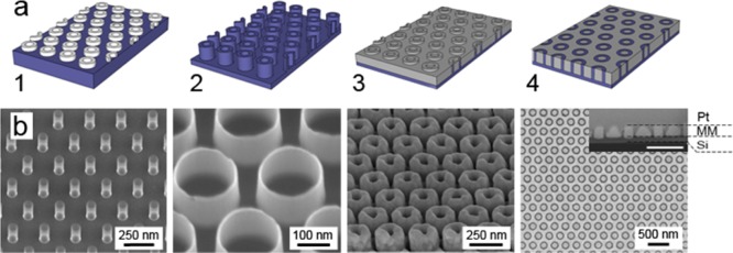
Coaxial metamaterials fabrication. (a) Schematic overview of the fabrication process: 1. EBL of HSQ on Si membrane. 2. Transfer structures into Si substrate with RIE. 3. Evaporate silver using a combination of EBPVD and Ar+ irradiance. 4. Polish the surface with FIB. (b) SEM images taken after different steps in the fabrication process. 1. Hollow pillars of HSQ after the EBL process. The walls are almost transparent for 5 keV electrons, which were used to take this image. 2. Si rings after RIE and HF dip. 3. Conformal deposition of evaporated silver. 4. Top view SEM image of the final metamaterial: Si appears as dark rings and is surrounded by silver. The inset shows a cross-section of the final metamaterial. The Si ring walls appear as very narrow dark lines in between the silver. Platinum was deposited in order to make the cross-section. The scale bar represents 500 nm.
Table 1. Dimensions of the Fabricated Metamaterial Fields as Measured from SEM Imagesa.
| sample # | Si cylinder outer diameter (nm) | coax pitch (nm) | Si cylinder thickness (nm) | metamaterial thickness (nm) | silicon support thickness (nm) |
|---|---|---|---|---|---|
| 1 | 168 | 250 | 15 | 91 | 49 |
| 2 | 168 | 250 | 13 | 43 | 88 |
| 3 | 163 | 200 | 13 | 40 | 105 |
| 4 | 166 | 300 | 13 | 52 | 74 |
| 5 | 168 | 250 | 15 | 66 | 66 |
| 6 | 150 | 300 | 15 | 137 | 40 |
The effective optical properties of the fabricated metamaterial are investigated by measuring its optical path length with a Mach–Zehnder interferometer. A schematic of the setup is shown in Figure 3a. Monochromatic laser light from an argon ion laser (λ = 351, 364, 458, 477, 488, 496, 515 nm) is split into a sample beam and a reference beam. The light in the sample beam is focused on the sample with a 0.45 NA objective. The transmitted light is collected by a second 0.45 NA objective and let to interfere with the reference beam on a photo diode. A piezo-electrically driven mirror in the reference arm is continuously moving back and forth over time using a sawtooth driving function. The intensity at the photodiode is then measured as a function of time. The inset of Figure 3a schematically shows the measurement procedure: first a measurement is done without the sample, and the absolute phase is deduced by fitting a sine function through the interference signal. Next, the metamaterial sample is placed in the sample arm and the absolute phase is determined again by fitting a sine function through the interference signal. The relative phase shift is then deduced by subtracting the absolute phase of the metamaterial sample from the absolute phase of the reference measurement. For every sample this procedure is repeated 300 times for each of the different wavelengths. Figure 3b shows histograms of the measured relative phase shift for all measured wavelengths for the sample with 168 nm outer diameter, pitch of 250 nm, and Si wall thickness of 15 nm (Table 1, sample 1). Since all measured data points are degenerate over 2π, all data is plotted within a phase range of 0–360°, which results in the discontinuities in Figure 3b. The width of the histograms is mainly due to a ∼25 nm uncertainty in the position of the piezoelectric mirror, consistent with the fact that the phase histograms are broader at shorter wavelengths.
Figure 3.
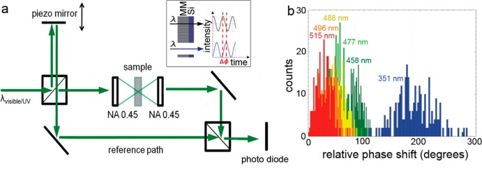
UV/vis Mach–Zehnder interferometry on coaxial metamaterial. (a) Schematic representation of the Mach–Zehnder interferometer used to determine the optical properties of the coaxial metamaterial. (b) Histograms built up from the collection of 300 measurements, for 6 different wavelengths for the sample with 168 nm Si cylinder outer diameter, pitch of 250 nm, and Si wall thickness of 15 nm (Table 1, sample 1).
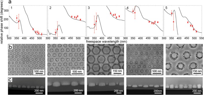
Figure 4a (red dots) shows the measured average phase shifts for 5 different coaxial metamaterial samples (Table 1, samples 1–5). The error bars in the data represent the standard deviation of the collection of 300 consecutive phase measurements. Top-view and cross-section SEM images of the 5 samples are shown in Figure 4b,c. Figure 4a shows several notable trends. First, for all five samples the measured phase shift strongly depends on wavelength, demonstrating the highly dispersive nature of the metamaterial. Second, small variations in the sample geometry lead to distinctly different phase shifts.
Figure 4.
Coaxial metamaterial phase measurements and geometries. (a) Experimentally measured phase shifts for different wavelengths on 5 metamaterial samples (Table 1, samples 1–5, red dots), derived from phase histograms as in Figure 3. Phase shifts obtained from FDTD simulations for the corresponding geometries are shown as solid lines. (b) Top-view SEM and (c) cross-section SEM images of the sample. A layer of Pt is deposited on the metamaterial samples to make the cross sections panel c.
Next, we compare the measured phase shifts with numerical finite-difference-time-domain (FDTD) simulations, performed with the experimentally measured dimensions of the different metamaterial samples as input. In the simulations the samples were illuminated with a plane wave pulse of linearly polarized broad band (λ = 300–700 nm) light under normal incidence. We extracted the relative phase shifts by taking the argument of the complex transmitted electric field and subtracting the phase of the reference (n = 1). The results are shown as solid lines in Figure 4a. Comparing the simulations with the experimental data we find very good agreement for all measured metamaterial samples. The trends of phase shift with wavelength are clearly reproduced in the simulations. Also, the different behavior measured for different sample geometries is clearly represented by the simulations. The slight differences between experiment and simulations can originate from a difference in the optical constants of the silicon and silver of the fabricated metamaterials and those used as input for the simulations. Also, errors in the determination of the thickness of the metamaterial or in the metamaterial dimensions would give rise to a difference between simulations and experiment, as does the fact that there is a small thickness gradient (∼10 nm) over the fields, originating from the final FIB polishing step. Simulations show that a thickness difference of about 10 nm in either the metamaterial thickness or the supporting Si layer thickness leads to a difference of 5–20° in the relative phase shift in the measured wavelength range. Finally we note that the measurements were performed using a numerical aperture of 0.45, causing an angular distribution of the incoming light, whereas the simulations are for normal incidence.
To further investigate the light propagation in the metamaterial we calculated the dispersion diagram for a single coaxial waveguide16 and compare it to FDTD simulations of a hexagonal array of coaxes. The dispersion diagram calculations were performed by solving Maxwell’s equations in cylindrical coordinates for a single, infinitely long coaxial silicon waveguide embedded in silver and are shown in Figure 5a. As expected, the cylinder exhibits both positive and negative mode indices; for both modes the real and imaginary values of the wave vector are plotted as solid and dashed lines, respectively. As can be seen, the negative-index mode (blue curves) shows lowest loss for wavelengths below 580 nm; the positive mode (red line) has lowest loss above 580 nm. From Figure 5a we conclude that the negative-index mode for individual coaxial waveguide is dominant in the wavelength range 440–600 nm. For the hexagonal array of coaxes we fitted a function of the form A·exp(ikzz) to the time-averaged real part of the Hy field distribution for six different wavelengths (400, 440, 460, 500, 600, and 700 nm), obtained from FDTD simulations under normal incidence. This allowed us to extract the wave vector (kz) of the light inside the metamaterial. The refractive index is then calculated by the ratio of the free space wave vector (k0) and the wave vector inside the metamaterial (kMM) derived from the field profiles. Table 2 shows the refractive indices deduced from the FDTD simulations together with the effective indices calculated from the dispersion diagram for single coaxial waveguide using the geometry of sample 1 (Table 1). As the analytical calculations and the numerical simulations use the same optical constants as input values, we ascribe the difference between the indices to the coupling between the waveguides. Using FDTD we also studied the time-dependence of the Hy-field (see movies in the Supporting Information) and observed a negative phase advance of light in the metamaterial at λ = 460 and 500 nm, again confirming the negative-index behavior of the metamaterial in this spectral range.
Table 2. Waveguide Mode Indices of Coaxial Metamaterial (Table 1, Sample 1) for Six Different Wavelengthsa.
| waveguide mode index |
||
|---|---|---|
| wavelength (nm) | single-coax dispersion | hexagonal array of coaxes |
| 400 | 2.35 | 2.17 |
| 440 | 0.11 | –0.12 |
| 460 | –1.63 | –1.49 |
| 500 | –4.67 | –4.74 |
| 600 | ||
| 700 | 10.54 | 13.61 |
Data are derived from calculated single-coax dispersion and Hy-field plots obtained with FDTD simulations. At λ = 600 nm the index is undefined since there is no propagating mode at this wavelength, making it impossible to extract the index using the method described above.
FDTD simulations were also used to simulate the transmission spectrum of the fabricated hexagonal coaxial metamaterial geometry (sample 1). Figure 5c shows simulated spectra for the experimental metamaterial geometry (red line), as well as simulations for the silicon supporting layer only (black) and the metamaterial film only (blue). The metamaterial-only simulation shows a transmission maximum around λ = 430 nm, which is consistent with the fact that the lowest losses are expected in this spectral range and that impedance matching between air and sample (with n ≈ 1) is optimal (see Figure 5a). At the transmission maximum the calculated propagation length is 1.6 μm. For the metamaterial/Si-support geometry (red curve) a sharp drop in transmission is observed for shorter wavelengths; this is mainly due to absorption in the Si support layer (black curve). For longer wavelengths the transmission decreases, even though the losses of the positive-index mode are small in this wavelength region. The low transmission in this spectral range is attributed to very inefficient coupling to the positive-index mode due to the poor field overlap of the (symmetric) modal field distribution of the positive-index mode with the incoming plane wave.
Finally, we measured the polarization dependence of the metamaterial index. We used interferometry as described above and used a half-wave plate to rotate the polarization of the incoming light in 10° steps over a range of 0–60°, where the 0° orientation corresponds to that along the y-axis in the SEM image of Figure 2c. Measurements were done on sample 6, with dimensions as given in Table 1. Figure 6 shows the measured phase shift at λ = 488 nm for each polarization. As above, the error bars correspond to the standard deviation of the collection of 300 consecutive phase measurements. Within the error bars we find no dependence of the phase shift on input polarization.
Figure 6.
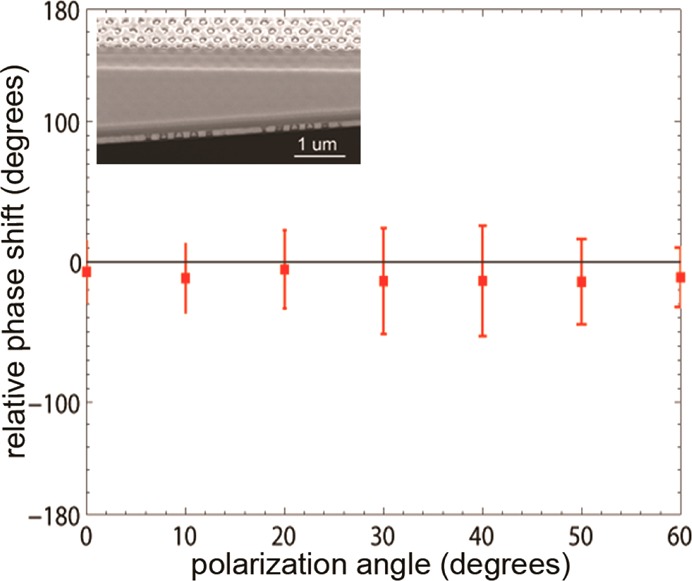
Phase shift as a function of polarization. Experimentally measured phase shift for different incident polarization angles at λ = 488 nm for sample 6 (see Table 1). Error bars correspond to the standard deviation of the collection of 300 consecutive phase measurements. Inset: cross-section SEM image of the metamaterial sample.
In conclusion, we have experimentally demonstrated a polarization-independent optical metamaterial composed of coaxial plasmonic waveguides. Using interferometry, the phase evolution of light inside the metamaterial was measured in the 351–515 nm spectral range. The data are in good agreement with numerical simulations showing a negative phase advance in the 440–500 nm spectral range.
Acknowledgments
We would like to thank Anja van Langen-Suurling from TU Delft for her help and support on the EBL process. This work is part of the research program of the Foundation for Fundamental Research on Matter (FOM), which is financially supported by The Netherlands Organization for Scientific Research (NWO). It is also supported by the European Research Council.
Supporting Information Available
Sketch of the metal infilling process and supporting movies. This material is available free of charge via the Internet at http://pubs.acs.org.
The authors declare no competing financial interest.
Supplementary Material
References
- Veselago V. Sov. Phys. Usp. 1968, 10, 509–514. [Google Scholar]
- Shelby R.; Smith D.; Schultz S. Science 2001, 292, 77–79. [DOI] [PubMed] [Google Scholar]
- Valentine J.; Zhang S.; Zentgraf T.; Ulin-Aliva E.; Genov D.; Bartal G.; Xiang X. Nature 2008, 455, 376–379. [DOI] [PubMed] [Google Scholar]
- Dolling G.; Wegener M.; Soukoulis C.; Linden S. Opt. Lett. 2007, 32, 53–55. [DOI] [PubMed] [Google Scholar]
- Rockstuhl C.; Zentgraf T.; Guo H.; Liu N.; Etrich C.; Loa I.; Syassen K.; Kuhl J.; Lederer F.; Giesen H. Appl. Phys. B: Laser Opt. 2006, 84, 219–227. [Google Scholar]
- Soukoulis C.; Linden S.; Wegener M. Science 2007, 315, 47–49. [DOI] [PubMed] [Google Scholar]
- Pendry J. Phys. Rev. Lett. 2000, 85, 3966–3969. [DOI] [PubMed] [Google Scholar]
- Pendry J.; Schurig D.; Smith D. Science 2006, 312, 1780–1782. [DOI] [PubMed] [Google Scholar]
- Edwards B.; Alù A.; Silveirinha M.; Engheta N. Phys. Rev. Lett. 2009, 103, 153901. [DOI] [PubMed] [Google Scholar]
- Chen H.; Chan C.; Sheng P. Nat. Mater. 2010, 9, 387–396. [DOI] [PubMed] [Google Scholar]
- Verhagen E.; De Waele R.; Kuipers L.; Polman A. Phys. Rev. Lett. 2010, 105, 223901. [DOI] [PubMed] [Google Scholar]
- Dionne J.; Verhagen E.; Polman A.; Atwater H. Opt. Express 2008, 16, 19001–19017. [DOI] [PubMed] [Google Scholar]
- Maas R.; Verhagen E.; Parsons J.; Polman A. ACS Photonics 2014, 1, 670–676. [Google Scholar]
- Xu T.; Agrawal A.; Abashin M.; Chau K.; Lezec H. Nature 2013, 497, 470–474. [DOI] [PubMed] [Google Scholar]
- Burgos S.; De Waele R.; Polman A.; Atwater H. Nat. Mater. 2010, 9, 407–412. [DOI] [PubMed] [Google Scholar]
- De Waele R.; Burgos S.; Atwater H.; Polman H. Opt. Express 2010, 18, 12770–12778. [DOI] [PubMed] [Google Scholar]
Associated Data
This section collects any data citations, data availability statements, or supplementary materials included in this article.


