Abstract
The evolution of micro/nanoelectronics technology, including the shrinking of devices and integrated circuit components, has included the miniaturization of linear and coaxial structures to micro/nanoscale dimensions. This reduction in the size of coaxial structures may offer advantages to existing technologies and benefit the exploration and development of new technologies. The reduction in the size of coaxial structures has been realized with various permutations between metals, semiconductors and dielectrics for the core, shield, and annulus. This review will focus on fabrication schemes of arrays of metal – nonmetal – metal nanocoax structures using non-template and template methods, followed by possible applications. The performance and scientific advantages associated with nanocoax-based optical devices including waveguides, negative refractive index materials, light emitting diodes, and photovoltaics are presented. In addition, benefits and challenges that accrue from the application of novel nanocoax structures in energy storage, electronic and sensing devices are summarized.
1) Introduction
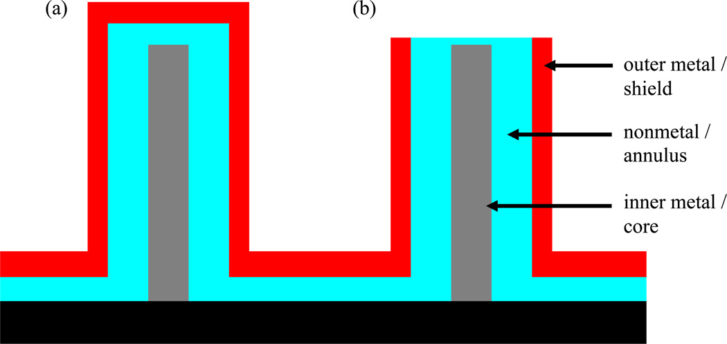
A nanocoax is a nanoscopic analog of a conventional coaxial cable or wire that consists of a metallic core, a cylindrical dielectric sleeve, and a solid or braided cylindrical outer metal shield. Conventional coaxial wires have been used to transmit signals essentially since the mid-19th century.1,2 After the successful synthesis and characterization of nanoscale-structures3–8 including nanorods, wires, and tubes, there has been interest in the realization of multilayer, coaxial nanostructures such as nanocoaxes.9 We consider coaxes that have annuli filled with any nonmetal, meaning solid, liquid, or gas, dielectric/insulator, or semiconductor. A nanocoax structure is created by adding these components, namely a dielectric or semiconducting annulus and metallic shield, in a radial direction onto a metallic, or at least highly conducting, nanowire or nanopillar, which serves as the core of the structure, as shown in Figure 1. By combining the different nanoscale layers of materials with a common axis in a radial direction, electronic and optical devices possessing various interesting functions have been created.
Fig. 1.
Illustration of different components of (a) a closed and (b) an open-ended nanocoax.
Over the last decade, a number of studies have been completed that explore optical properties of nanoscale subwavelength structures and their fundamental applications, in order to understand near-field optics and to construct photonic devices.10–17 Among the different subwavelength structures that have been analyzed, the nanocoax is of particular interest, as this structure is considered to have high transmittance to visible light and is a promising structure for deep-subwavelength, low-loss propagation of plasmonic and photonic radiation modes at optical and infrared frequencies.12,15,18 The nanocoax geometry already has been employed in a variety of applications including photovoltaic (PV) solar cells, optical nanoantennas, negative index materials, and light-emitting fibers.19–24 For example, the ability of a nanocoax to have its dielectric replaced with a semiconducting / PV material allows for the absorption or generation of light as it propagates along its axis, yet have photogenerated electrical current flow radially between the inner and outer metals. This allows, in principle, for increases in solar cell and photodiode efficiency.25–33 In this structure, efficiency of transport (or collection of charge carriers) and absorption of light can be controlled by simply varying the radial thickness of the PV material and the height of the coax. Because the PV layer can be extremely thin and still absorb light, this structure is amenable to polymer and organic solar cells as well.32,33
A nanocoax PV array can also have unique biological sensing applications. The architecture can potentially be used in a high resolution optoelectronic retinal prosthetic system to provide electrical stimulation of the retina and produce visual percepts in blind or visually-impaired patients suffering from, e.g., macular degeneration or retinitis pigmentosa.34 Other optical phenomena, such as surface plasmons and electromagnetic oscillations at the interface between a dielectric and a conductor of a nanocoax, could make it possible to overcome the diffraction limit of light in the field of optical imaging.35
The unique applications of the nanocoax are not necessarily due to new physical properties introduced by the structure. The large surface area and associated nanoscale gap between electrodes render possible some very useful applications in areas other than sensing, such as in energy storage devices. For example, because the capacitance of a capacitor depends on the surface area of its electrodes and the distance between them, a significant increase in capacitance of a capacitive storage device can be achieved by building arrays of densely-packed, high aspect ratio nanocoax-based dielectric capacitors, as the coaxial geometry optimizes both enabling parameters.36–38 Similarly, in the case of electric double layer (EDL) capacitors, the capacitance is directly proportional to the effective surface area of its electrodes.39 The surface area of the electrodes can be increased using a hollow or high-K dielectric nanocoax architecture that facilitates high capacity capacitors in a small volume. In other energy storage devices, such as batteries, the conversion and storage capacity depends upon chemical interactions that occur at the electrode-electrolyte interface and the transport of ions between electrodes.40 In such cases, beside the aforementioned effect of high electrode surface area, nanoscale structures can facilitate an increase in the transport rate of ions between electrodes, which can enhance the efficiency and cycling performance of the devices.
The high surface area per unit volume makes the nanocoax structure a strong candidate for chemical and biological sensing applications and provides a way to scale the active sensing volume. The nanocoax structure renders possible spatially-resolved biological sensing because the size of an individual nanocoax is comparable to or smaller than that of many biological systems. A combination of 3D nanocoax structures and innovative signal transduction technologies can improve the limit of detection and sensitivity capabilities that exist in nanostructured sensors.41–43 In particular, a nanocoax structure with a porous dielectric or partially hollow cavity annulus is emerging as a promising candidate for sensitive electrical, optical and electrochemical sensors.44–46 In addition, the nanocoax structure has also been used to make memory cells and probes of electrical devices.47–49
In this article, we attempt to be comprehensive with respect to the types of nanocoaxes that are possible and the structure-property relationships that emerge as a result. The description of nanocoax fabrication and application contains a few representative examples to highlight the potential for new functions that arise from a nanocoax geometry. Applications that lack a quantitative confirmation of technical or scientific benefit from the nanocoax structure are noted but not discussed comprehensively. This review does not include fabrications and applications of the other concentric, nanoscale heterostructures comprised of all-semiconducting materials, which alone have enough importance and scope to require many separate reviews,50–52 but which are not, strictly speaking, nanocoaxes.
2) Fabrication
Several approaches have been used for synthesizing nanostructures, including nanotubes, nanowires, and nanopillars.5,7,53,54 Certain fabrication steps are then added to form multi-component nanocoax structures. The components of a nanocoax, namely the core, annulus and shield, are made by changing parameters, materials and methods during its fabrication process. In recent years, a number of material deposition technologies such as arc discharge, laser ablation, thermal evaporation, physical vapor deposition (PVD), chemical vapor deposition (CVD), plasma enhance chemical vapor deposition (PECVD), atomic layer deposition (ALD), focused ion beam (FIB), electrochemical deposition, and chemical synthesis have been used to make nanocoax structures. Here, the fabrication processes of nanocoaxes are categorized into two groups, template-free and templated methods, based on starting structures.
(2.1) Template-Free Method
The template-free method does not require any scaffold, as the core of the coax structure itself provides the support for its other two layers. Metallic nanowires and nanotubes can been used as cores of a nanocoax. Particularly, carbon fiber is one of the more commonly incorporated materials for a core. Suenaga, et al. employed an arc discharge method with a graphite cathode and a HfB2 anode in N2 atmosphere, to synthesize C-BN-C nanowire heterostructures of diameter up to 12 nm.9 This C-BN-C geometry closely resembles a metal-insulator-metal nanocoax geometry. Using multiwalled carbon nanotubes (MWCNT) and controllable chemical substitution reactions in a chemical synthesis method, a novel coaxial C-AlN-C nanotube of outer diameter 45–50 nm was made by Yin, et al.55 In this case, a mixture of Al2O3 powder and CNT was heated in a furnace with a flow of NH3, where carbon of the MWCNT acts as the reducing agent and is replaced by the AlN. Guo, et al. used surface functionalization and chemical synthesis processes to make different CNT-core coaxial nanocables of diameter 100 nm, such as CNT-TiO2-Ag, CNT-TiO2-Au, CNT-TiO2-Pd and CNT-TiO2-Pt.56 In this room temperature process, the thickness of the TiO2 was controlled by changing the weight ratio of CNT and Ti(OC4H9)4, the precursor of TiO2. The outer metal of the coax was deposited on a TiO2 layer via a chemical reduction of the corresponding metallic compound. A similar coaxial structure, CNT-SnO2-Au with a diameter of ~50 nm, was made by growing SnO2 on the surface of a CNT through the hydrolysis of SnCl2 followed by Au deposition onto the SnO2 layer via reduction of HAuCl4.57
Other well known deposition techniques, such as ALD, CVD, PECVD and PVD were used to deposit dielectric or semiconducting material and the outer metal layer on vertically aligned CNT or carbon nanofibers (CNF) arrays to make CNT-SiNx-Cr,48 CNT-Si-ITO,27 CNT-Al2O3-Al15,45 and CNT-CdTe/CdSe-ITO25 coaxial nanostructures of different diameters.
Figure 2 shows a schematic along with scanning electron microscope (SEM) and transmission electron microscope (TEM) images of a single unit from an array of open-ended CNF-Al2O3-Al nanocoaxes, as reported by Zhao, et al.45 To fabricate these arrays, they deposited Al2O3 and Al layers on a vertically-oriented CNF array, the latter prepared by PECVD, as first demonstrated by Chen, et al.58 As an initial coating outside the CNTs, 10 nm Al2O3 was deposited by ALD to prevent potential electrical shortages between the inner and outer coax electrodes. Following this, reactive sputtering was employed to apply ~100 nm porous Al2O3 by introducing O2 during Al sputter deposition. Al of ~250 nm thickness was sputter deposited for the outer coax electrode. The top end of the coax was then removed to make open-ended nanocoax structures. Before polishing, mechanical support for each coax was provided by spin-coating SU8-2002 photoresist, cured at 200°C for 1 h, then polishing with a vibratory polisher until the cores of the nanocoax structures were fully exposed.
Fig. 2.
(a) Schematic of the cross-section of a nanocoax. (b) SEM image of top view of a open ended-nanocoax (c) cross-sectional TEM image of a nanocoaxial capacitor with ~150 nm diameter CNF inner electrode, ~10 nm and ~100 nm thick layers of nonporous and porous Al2O3 respectively and ~ 250 nm thick outer electrode. Reproduced with permission from Ref. 45.
The examples noted above were for C-core nanocoax structures. Template-free metal-core nanocoax structures of Cu-Cu2O-C with diameter ~130 nm were made using chemical synthesis and vapor deposition method.37 In this process, a hydrothermal method was used to make a polyvinyl alcohol (PVA)-coated Cu nanowire. Thermal oxidization of Cu and carbonization of PVA were then performed to make a Cu-Cu2O-C structure. Other techniques, such as optical lithography followed metal deposition and chemical etching, have been employed to fabricate arrays of nanocoaxes over relatively large areas. Fan, et al. used interference lithography followed by lift-off and anisotropic O2 plasma etching to fabricate arrays of 100 nm high nanocoaxes with Au inner and outer electrodes, separated by a hollow annulus of controllable width.59,60 Recently, wafer-scale fabrication processes for arrays of open-ended Au-Al2O3-Au micro/nanocoaxes about 200 nm high and with sub-10 nm thick dielectric annulus were reported.61,62 In these processes, a thin layer of Al2O3 was deposited on photolithographically-defined micro/nanosized metal structures, followed by deposition of an outer metal and removal of the uppermost part of the outer metal. In addition, mass production methods such as electrospinning – a process that could stretch a viscous, conductive fluid into a thin jet via electrostatic force – were used to fabricate coaxial structures with diameters ranging from several micrometers down to tens of nanometers.63,64
(2.2) Template Method
In the template method, predefined nanostructures such as nanopores or nanopillars can be used as supportive templates for subsequent layers forming nanocoaxes. Nanocoax structures employed in many applications have in fact been fabricated using various kinds of templates. For example, porous anodic aluminum oxide (AAO), a source for an array of self-ordered nanopores of ultrahigh density and high aspect ratio, has been used as an economical and efficient template for the fabrication of nanowire arrays.65 Banerjee, et al. used AAO templates to make arrays of nanoscale coaxial capacitors.36,38 To fabricate these arrays, thin and conformal metal and dielectric films were deposited in the pores of the AAO template using CVD or ALD.
Figure 3 shows SEM images of the top, side and cross-section of a hexagonal array of a nanocoaxial capacitor made by the application of successive ALD layers of metal (TiN), insulator (Al2O3) and metal (TiN) within AAO nanopores. In the cross-sectional view, a 25 nm diameter TiN inner electrode, 6 nm thick Al2O3 dielectric layer, and 5 nm thick TiN outer electrode can be seen.
Fig. 3.
SEM images of (a) top view of the metal-insulator-metal structure in AAO template having hexagonal unit cell, (b) side view of metal-insulator–metal structure in AAO template, and (c) cross-sectional view of a nanocoaxial capacitor with ~25 nm diameter inner electrode of TiN, ~6 nm thick dielectric layer of Al2O3 and ~5 nm thick outer electrode of TiN. Reproduced with permission from Ref. 36.
Other lithographically-prepared nanostructures have been employed to make nanocoax structures. Lipomi, et al. used soft lithography66 for replica molding of arrays of polymer (UVO-114) pillars, followed by sputtering and electrochemical growth for deposition of thin films of metal (Au), and the conducting polymer polypyrrole (Ppy), respectively. In addition, nanoskiving and plasma etching were used to make an array of open-ended and hollow annuli nanocoaxes.67
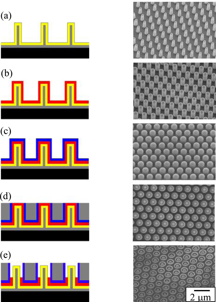
Rizal, et al. used similar processes to make arrays of nanocoaxial structures. They used nanoimprint lithography (NIL)66 to fabricate arrays of nanocoaxes using SU-8 replicas of Si nanopillar arrays as templates.68 They metallized the surfaces of the SU-8 nanopillars using PVD, followed by deposition of dielectric and outer metal layers. Different dielectrics were deposited using different methods, including ALD, PECVD and sputtering, to deposit films anywhere between 10 nm and 200 nm (measured radially) of porous or nonporous dielectrics such as Al2O3, SiO2, Si3N4, polymer, amorphous silicon (a-Si), etc. Next, an outer metal film of typical thickness 20–100 nm was deposited to form nanocoax arrays. To make the open-ended coax array, the top end of the outer metal was removed by either a chemical or a mechanical polish method. Figure 4 shows schematics and SEM images of the steps involved during the fabrication of these open-ended nanocoax structures. Similar techniques were used to make Au-based nanocoax arrays for a possible plasmonic nanosensor.44
Fig. 4.
Schematic and SEM images of fabrication process for arrays of open-ended nanocoaxes of 1.3 µm pitch and 2 µm height. (a) Inner metal coating (Cr ~150 nm). (b) Dielectric coating (Al2O3 ~200 nm). (c) Outer metal coating (Au ~120 nm) (d) SU-8 coating and mechanical polishing. (e) Etching of dielectric (depth of cavity ~500 nm). Reproduced with permission from Ref. 68.
Im, et al. employed colloidal, lithographically–assembled, polystyrene nanospheres as a template for the fabrication of arrays of Ag-Al2O3-Ag nanocoaxes with periodicities ranging from 400 to 600 nm. They deposited 200 nm layers of Ag and 10 nm of Al2O3 on the surface of nanospheres using PVD and ALD, respectively, and then etched the top of outer Ag layer using ion milling to make open-ended nanocoax arrays.69 Using a buffer oxide etchant solution, Al2O3 was etched down to make arrays of nanocoaxes with partially hollow cavity annulus.
Naughton, et al. used nanopillar arrays of several materials such as crystalline and amorphous silicon, silicon oxide, aluminum, CNTs, and a variety of polymers as templates to make nanocoax-based solar cells. They fabricated Ag-Si-ITO structures by depositing Ag, Si and ITO on the surface of each pillar using PVD and CVD processes.28,29 Recently, Kim, et al. used arrays of glass nanocones fabricated via a photolithography-free nanopatterning method to make Ag-Si-ZnO:Al nanocoax solar cells with a 150 nm thick layer of a-Si, as shown in Figure 5.31 In this method, Sn nanospheres with diameters 20 nm to 1.2 µm, self assembled during the rapid thermal annealing of Sn films on glass substrates, were then used as an etch mask for deep reactive ion etching to form glass nanopillars. These nanopillars were subjected to chemical etching to taper them into glass nanocones, with subsequent coatings to form nanocoax-like structures.
Fig. 5.
(a) Schematic and (b) SEM images of arrays of nanocoaxial a-Si:H solar cell fabricated on glass nanocone. (c) High resolution SEM images of the cross section of each coax in (b), showing different layers, namely 150 nm of ZnO:Al, 150 nm of a-Si, and 50/120 nm of Ag/ZnO:Al in a radial direction. Reproduce with permission from Ref. 31.
Carny, et al. made Ag–peptide–Au coaxial nanocables from soft biological templates.70 In this process, a peptide that self-assembles into nanotubes served as the template and insulator. The insides of the nanotubes were then filled with silver by incorporating Ag+ ions into the tubes and then reducing those to silver metal. Agpeptide-Au nanocoaxes were formed by attaching gold nanoparticles to the outer walls of the peptide backbone through a thiol-terminated peptide linker and by subsequent reduction of gold ions onto the peptide-bound gold nanoparticles.
3) Applications
(3.1) Optical Devices
In the last decade, considerable efforts have been undertaken to understand the propagation of electromagnetic fields and other optical properties for possible applications of the nanocoax structure. In this review, we discuss some representative work in this arena.
(3.1.1) Waveguides
Multiple theoretical works focused on the propagation properties in subwavelength coaxial waveguides have been published.10,12,16,71–76 An early analysis comes from Baida, et al.,77 who demonstrated theoretically that propagation of radiation in a subwavelength coaxial waveguide can be made by photonic and/or plasmonic modes, depending on the wavelength of the excitation field and the inter-electrode spacing (annulus width). The study regarding different order modes showed that the cut-off wavelength is strongly dependent upon the coaxial geometry, as expected, but particularly on the inter-electrode spacing. Specifically, very tight inter-electrode distances resulted in long propagation distances. In this work, the hypothetical sample was made of Ag and the inner electrode had a radius of 75 nm, while the outer electrode had a variable radius in order to study its effect on the propagation of an electromagnetic field.77 Figure 6 shows the intensity distribution of the first (a, c, e, g) and second (b, d, f, h) plasmonic modes at the cut-off wavelength as a function of the inter-electrode distance. There, it can be seen that, for the fundamental transverse electric mode TE11, light is essentially confined in the gap between the two metallic parts of the waveguide.
Fig. 6.
Intensity distributions in a section of the waveguide for different values of the outer radius, while the inner radius is 75 nm (a, c, e, g) correspond to the first and (b, d, f, h) the second plasmonic modes Reproduce with permission from Ref. 77.
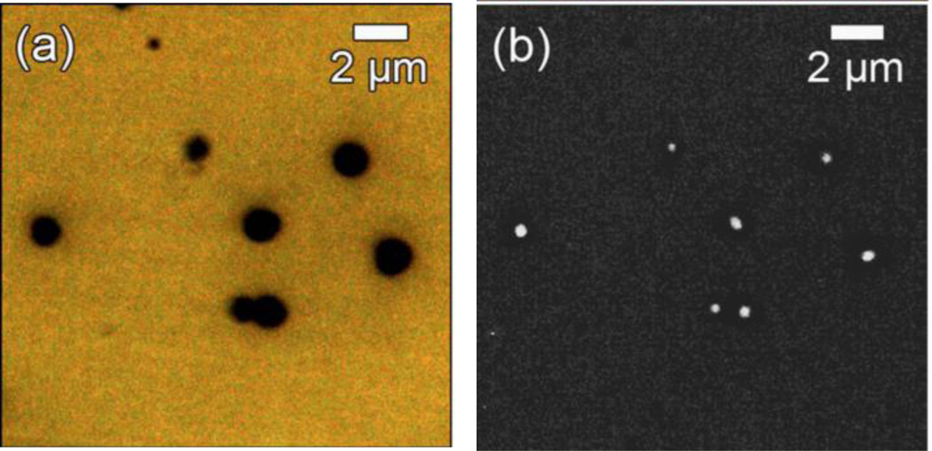
Later, Poujet, et al. completed an experimental study of the transmission through a subwavelength coaxial aperture array for wavelengths in the visible range.78 Experimentally, an efficiency of about 20% was reported for the transmission in a coaxial structure with 250 nm inner electrode diameter, 330 nm outer electrode diameter, 600 nm pitch, along a longitudinal distance of 100 nm. These values were less than numerical predictions of 60% efficiency at 1330 nm wavelength for Au and 80% efficiency at 700 nm wavelength for Ag-based nanocoaxes. Likely the first experimental work on subwavelength coaxial waveguides in the visible spectrum was reported by Rybczynski, et al.15 In this work, the observation of propagated light using optical microscopy was reported. It was shown that white light can propagate without a noticeable cut-off wavelength and that longer wavelengths propagated for longer distances relative to shorter wavelengths. For the given dimensions, this was an indication that plasmon modes propagating inside the waveguide were reduced to the usual transverse electromagnetic (TEM) mode. One of the main results was that propagation could be over distances as long as 50 µm. In the reported structure, the inner electrode was a multi-walled carbon nanotube with a 100 nm diameter, coated with 100 nm of Al2O3 and the outer electrode was a 100 nm thick layer of Cr. Figure 7 shows the main experimental results.
Fig. 7.
Optical microscope images of light (a) reflected off nanocoaxes under front white illumination and (b) transmitted through nanocoaxes under back illumination. Reproduced with permission from Ref. 15.
In 2008, Peng, et al. showed theoretically that a subwavelength coaxial waveguide can support a plasmonic mode that resembles the TEM mode when the excitation field has a much longer wavelength than the plasma wavelength of the metal used in the electrodes.79 Such a mode can propagate without a cut-off wavelength, resulting in the conceptual extension of the radio-wave coaxial waveguide. In this report, the inner and outer electrodes had diameters of 50 nm and 150 nm, respectively. Both electrodes were made of Ag, while the inter-electrode spacing was filled with air for simplicity in the calculations, confirming the results obtained by Rybczynski, et al.15 Later, Kempa, et al. showed theoretically that an array of subwavelength coaxial waveguides can produce efficiency as high as 90% in far field transmission when an optical field is coupled via a TM00 mode, which at long wavelengths range is reduced to the TEM mode.80 In that work, the coaxial structure was simulated with Al inner and outer electrodes and air inter-electrode space.
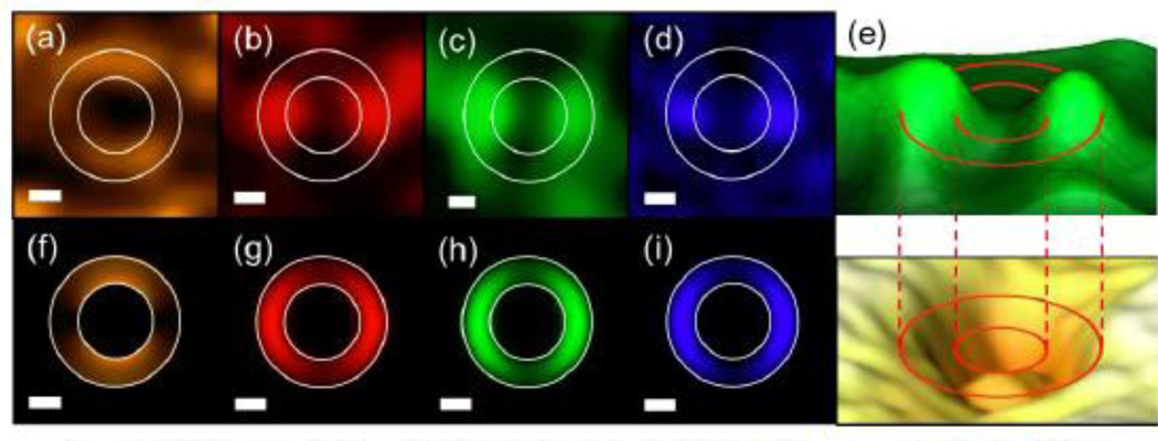
Because these subwavelength coaxial waveguides do not experience a cut-off wavelength, a photonic light wave that is transmitted through does so without a loss of subwavelength resolution. More recently, Merlo, et al. reported the observation of different nature (i.e. photonic and plasmonic) propagating modes of visible and near infrared light in Au-Al2O3-Au nanocoax structure. The observed and calculated images of the propagated modes are as shown in Figure 8. They also calculated the dispersion relation and propagation length for studied modes. Using near-field scanning optical microscopy, they observed TE11 and TE21 modes in the near infrared and TE31, TE41 and TM11 modes in the visible range. Note that the TE11 and TE21 modes have plasmonic character while the TE31, TE41 and TM11 modes are photonic, i.e. they lie above the light line in Figure 9 (a). The calculated values of the propagation length (Figure 9 (b)) indicate that the TE11, TE21 and TE31 modes can propagate along the full nanocoax length (~2 µm) and couple to the far field, in the spectral range analyzed experimentally.
Fig. 8.
NSOM-measured (a – d) and calculated (f – i) images of propagated modes in a nanocoax structure. The wavelengths were 850 nm (a, f), 660 nm (b, g), 532 nm (c, h) and 473 nm (d, i). In all cases, the polarization is in the vertical direction, the scale bars represent 200 nm and circles represent the inner and outer radii of the coax annuli. (e) Three-dimensional representation of the nanocoax topography via AFM (lower) and the corresponding near-field intensity (upper) for 532 nm wavelength. Reproduced with permission from Ref. 18.
Fig. 9.
(a) Calculated dispersion relations of modes propagating in a nanocoax structure. The dashed lines represent the frequencies employed (excitation wavelengths) and the shaded area represents the zone where plasmonic modes appear (i.e. separated from photonic modes by the light line ω = kc). (b) Calculated propagation lengths for the studied modes. The dashed lines represent the wavelengths used and the shaded region indicates the length of the nanocoax structure. Note the logarithmic scales. Reproduced with permission from Ref. 18.
Waele, et al.23 studied theoretically and experimentally a single nanocoax and determined the plasmon dispersion relation for different sizes of subwavelength coaxial waveguides. They concluded that the dispersion depends strongly on the dielectric material that fills the inter-electrode spacing and the dielectric that surrounds the subwavelength coaxial waveguide, as well as the coax length. The samples reported in their work were fabricated by FIB with fixed outer electrode diameter of 175 nm, with varying inter-electrode spacing ranging from 20 nm to 100 nm and varying thickness Ag layer ranging from 285 nm to 485 nm. Figure 10 shows the measured dispersion data as well as calculated index-averaged dispersion relations for different dielectrics filling the inter-electrode space.
Fig. 10.
Experimental dispersion and calculated index-averaged dispersion relations (red drawn lines). The inter-electrode distance is 50 nm filled with air (a) and spin-on glass (SOG) (b). Light lines for air (a) and SOG (b) are shown as dotted green lines and the plasmon dispersion is the dashed orange curves at a flat Ag/air interface (a) and Ag/SOG interface (b). Reproduced with permission from Ref. 23.
Kozina, et al. investigated theoretically the propagation of electromagnetic fields in coaxial waveguides with different geometries of the inner core, those being circular and elliptical cross sections.81 It was found that the waveguides with elliptical cross section inner electrodes produced faster group velocity than those with circular cross sections, when a dipole-like field is propagated. On the other hand, the TEM mode did not change notably with a change in shape of the inner electrode cross section. As a result, an inner electrode with two orthogonal ellipse cross sections with dual-polarized field distribution can be propagated. In that report, the inner and outer electrodes were Ag and the inter-electrode spacing was filled with air or glass.
Using the propagation inside a subwavelength coaxial waveguide, Weber-Bargioni, et al. demonstrated the use of a near-field probe based on a coaxial structure by modifying an atomic force microscope AFM tip.24 A similar probe was simultaneously used as probe for topography and Raman spectroscopy, combining the enhanced field and the localized plasmonic antenna. In that report, the AFM tip was made of SiN coated with 120 nm of Au and the coaxial structure was fabricated by FIB with inter-electrode distance 20 nm filled with air.
In addition to above mentioned waveguiding applications, Saleh, et al. theoretically proposed that coaxial structure with nanometer-sized annuli can be used as optical traps for nanoscale specimens.16 They reported that a particle of size as small as 5 nm can be trapped by near field transmitted light through a 150 nm tall, 120 nm inner diameter and 25 nm annulus width Ag-SiO2-Ag coax, illuminated with a linearly polarized plane wave. They also demonstrated that by tapering the thickness of the annulus of the coax, the trapping dimension can be lowered to sub-2 nm.
(3.1.2) Metamaterials and Plasmonic Crystals
Another application of a nanocoax is as a metamaterial. The enhanced transmission of plasmonic modes propagated in arrays of subwavelength coaxial waveguides can be considered a metamaterial phenomenon. Burgos, et al.21 reported a theoretical description of a metamaterial based on coaxial waveguides that showed an effective negative refractive index in a wide bandwidth of the electromagnetic spectrum. The material developed had functionality independent of the polarization of the excitation field and was useful over an angular range of 50°. The negative refractive index was characterized by a negative refraction and backwards phase propagation. In that study, an array structure had hexagonal, close-packed geometry with a pitch of 165 nm, inner and outer electrodes made of Ag with diameters of 75 nm and 100 nm, respectively, and inter-electrode spacing of 25 nm filled with GaP.
Figure 11 shows the real part of the y-component of the magnetic field interacting with the proposed metamaterial. Note that inside each coax, the direction of energy flow S is found to be antiparallel to the phase velocity k, which is a signature of a negative refractive index material.
Fig. 11.
Calculated magnetic field distribution Re(Hy) in the metamaterial. The wavelength used was 483 nm at incidence angle of 30°. Arrows denote the direction of energy flow S and phase velocity k. Reproduced with permission from Ref. 21.
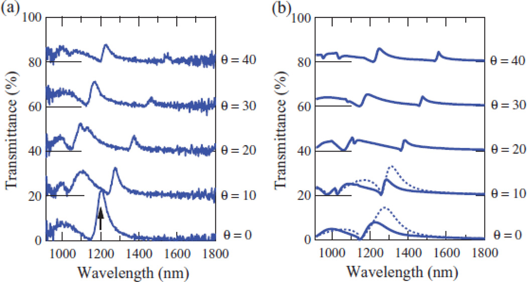
Iwanaga, et al.22 demonstrated experimentally that a plasmonic crystal can be constructed from a hexagonal array of nanocoaxes, and that the local electromagnetic field is enhanced several times over that of one produced by plasmonic crystals with non-coaxial structures. Changing the incidence angle resulted in a red-shift in the transmittance spectra due to the different propagated modes excited in the coaxial structures. The reported structure was made by electron beam lithography with hexagonal pitch of 900 nm. The inner and outer electrodes had diameters of 150 nm and 350 nm, respectively, in a 150 nm thick Al film. Figure 12 shows the experimental and calculated transmittance produced by the plasmonic crystal.
Fig. 12.
Experimental spectra (a) and calculated (b) transmittance of p-polarized light. The offset in the curves represents the spectra at different incidence angles. Reproduced with permission from Ref. 22.
Finally, Ndao, et al. showed the fabrication and optical characterization of slanted coaxial arrays milled in a silver film.20 The registered optical transmission efficiency for this slanted coaxial array was 70% for light transmitted to the far field by the TE11 mode, and 20% for the TEM mode. The wavelength at which maximum transmission occurred was controlled by the thickness of the metallic film, due to the properties of the propagation inside the coaxial structures. In their report the coaxial structure was fabricated by FIB in a 190 nm thick Ag layer. The structure had inner and outer electrode diameters of 95 nm and 295 nm, respectively, while the inclination angle was 31.4°. Figure 13 shows the dispersion relation and the effective refractive indexes for the TE11 and TEM modes for this work.
Fig. 13.
(a) Schematic representation of the coaxial structure. (b) Dispersion curves for waveguides made of Au (red) and Ag (blue). Effective refractive indexes of TE11 (c) and TEM (d) as function of the wavelength. Reproduced with permission from Ref. 20.
(3.1.3) Light Emitting Diodes
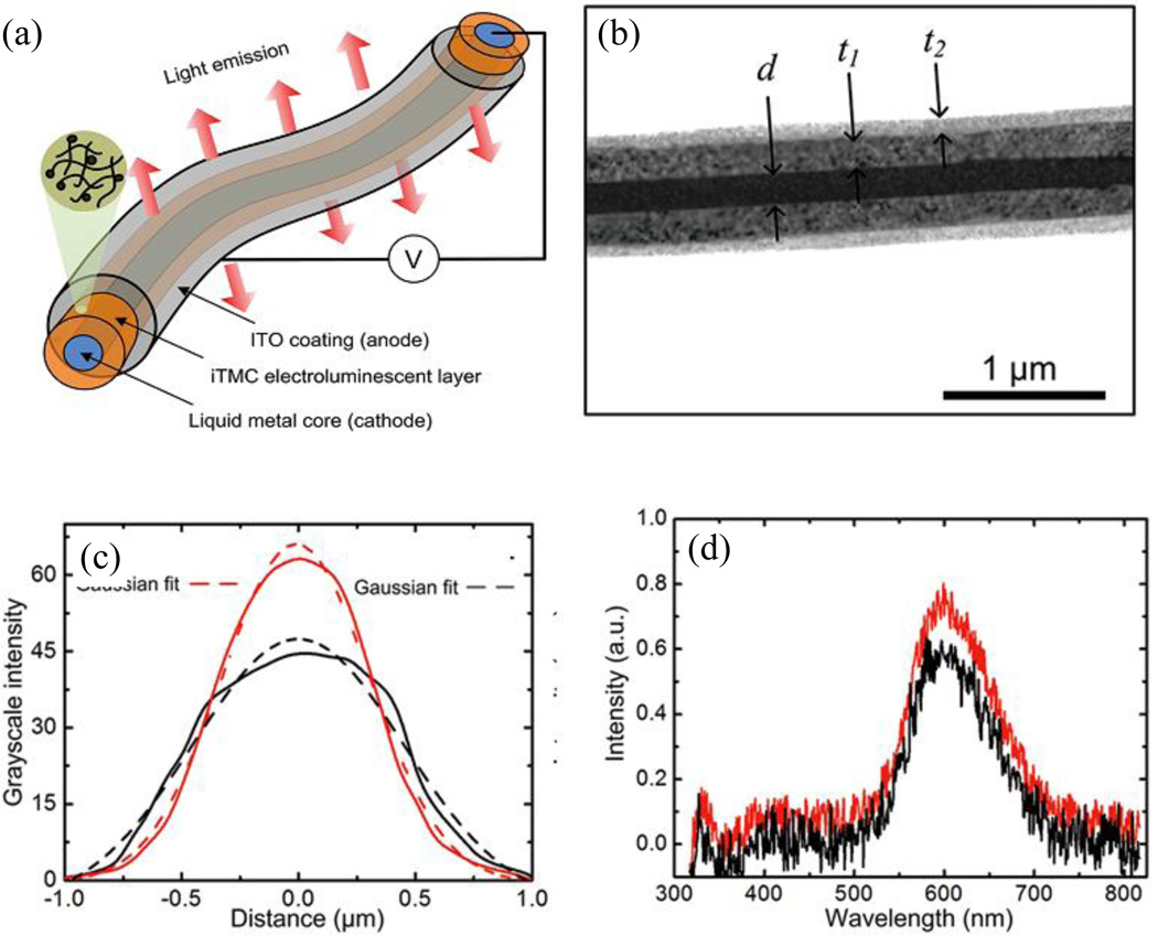
Nanocoaxial structures have been used to make optoelectronic devices such as photodetectors and light emitting diodes (LED) compatible with current semiconductor platforms. The two fundamental functions characterizing optoelectronic devices are photo-detection and photo-emission. As a detection mechanism, a coaxial structure exploits the intrinsic enhancement of the electric field in the active (dielectric) layer, which can lead to a reduction of the detector’s operating voltage and response time and an increase in sensitivity compared with those of its bulk counterpart. Moreover, in this geometry, the strong radial fields spatially separate the charges (electrons and holes), thereby reducing the recombination rate and increasing the photoconductive gain.50,82 These coaxial structures have been used to make organic light–emitting diode (OLED) devices. Yang, et al. made a mechanically flexible, lightweight, submicron diameter coaxial structure with a galinstan liquid metal core surrounded by ionic transition–metal complex (iTMC)-based organic electroluminescent material drawn from a mixture of ruthenium(II) tris (bipyridine)[Ru(bpy)3}2+(PF6)−2] and polyethyl oxide (PEO) and transparent metal oxide outer electrode (ITO), as shown in Figure 14.
Fig. 14.
(a) Schematic of the an ionic transition-metal complex (iTMC)-based flexible nanocoaxial OLED. (b) TEM image cross section of a coaxial OLED with inner electrode of diameter d ~200 nm, iTMC- polymer of thickness t1 ~ 200 nm and outer metal of thickness t2 ~ 70 nm. (c) Grayscale intensity profile from a 2 µm-long line OLED with 212 nm (red) and 317 nm (black) thick layers of iTMC-polymer. (d) Electroluminescence spectra of light emitted from OLEDs in (c). Reproduced with permission from Ref. 63.
It is important to note that in this self-supported coaxial structure, iTMC provides all three ionic space charge effects – charge injection, charge transport, and emissive recombination. The use of the liquid metal electrode gave a sharper metal-organic interface than those obtained from vapor-deposited metal electrodes. In these OLEDs, the emission intensity was controlled by tuning the thickness of the active layer (iTMC) of the coax. However, the characteristic emission wavelength was independent of the coax dimension as shown in Figure 14(c) and (d).
(3.1.4) Photovoltaics
Photovoltaic (PV) technology is receiving considerable attention for its potential application in sustainable energy production. Since the introduction of the first crystalline Si (c-Si) solar cell83 some 60 years ago, PV technology has undergone revolutionary developments. For an efficient solar cell, the active layer needs to be an efficient absorber of light and must allow for the efficient extraction of light-generated charge carriers. However, there is a trade-off between being optically thick and electrically thin in conventional thin film solar cells, because the light absorption path and carrier extraction paths are one and the same. Efficient conventional c-Si solar cells, which have planar junctions of p-type and n-type c-Si and charge carriers that are collected along the light path, require relatively thick (~200–500 µm) and high-purity Si film. The requirements for large amounts of high-purity Si materials contribute to the cost of c-Si PVs. Extensive attention has been paid to developing less expensive thin-film solar cells,84 such as amorphous Si (a-Si),85 polycrystalline Si,86 cadmium telluride87 and polymer based PV, among many others.88 Still, these options are not yet a cost-competitive alternative to C-Si, let alone to traditional fossil fuels.
However, in recent years, a number of new strategies that may substantially improve the performance and lower the cost of PV have emerged. Indeed, many nanotechnology-based enhancements for the performance of solar cells have been proposed.89 Among them, nanostructures such as nanowires, nanorods and nanocones, all essentially configured in a nanocoax geometry, are emerging as promising candidates for building efficient PV devices.90–93 In particular, an array of vertically aligned nanocoax solar cells, containing a large number of sub-cells connected in parallel as well as each cell solar irradiated in parallel with the p-n junction, could relieve the optical–electrical conundrum to a certain extent because of its unique geometrical features.28 The essence of this 3D nanocoaxial geometry is the orthogonalization of the light and carrier extraction paths inside the PV material, which simultaneously enables strong photon absorption and efficient carrier collection. When an array of vertical nanocoaxes with radial p-n junctions in the annuli is further prepared with an optically-transmitting outer conductor (e.g. ITO) e, additional enhancements in optical absorption can arise due to strong intercoax (as opposed to intracoax) scattering and trapping/waveguiding of light . The amount of active PV material required to absorb a given amount of light could be much less than in an equivalent area conventional planar PV device.94 As a result, small amounts of PV material can be sufficiently optically thick in the longitudinal direction to capture long wavelength radiation that otherwise has a long penetration length in the absorber. At the same time, it can be sufficiently electrically thin in the radial direction to enable a short minority-carrier transport length.95 This short carrier transport distance allows high carrier collection efficiency even for low quality (i.e. noncrystalline) and low cost PV materials like a-Si, which has a low minority carrier diffusion length (~100 nm). Therefore, nanocoax-based solar cells with radial p-n junctions of PV materials have the potential to meet both cost and efficiency challenges faced by PV technology.
Several attempts have been made to examine the performance of coaxial geometry based solar cells. However, the reliable performance of a single nanocoax solar cell has not yet been reported. Even before exploring the performance of a single nanocoax solar cell, several approaches have been taken to make a more practical solar cell device consisting of an array, where the metallic inner and outer shells act as proximity electrodes for PV materials sandwiched between them. For example, Camacho, et al. reported an array of vertically aligned CNT-CdTe/CdS–ITO nanocoax solar cells.25 They compared the performance of coaxial devices with that of planar silicon cells for various azimuthal angles of the light source. Interestingly, when the angle of incidence was changed from ‘high noon,’ orthogonal incidence to an oblique angle of 45°, the “efficiency” of the coaxial cell doubled from ~3.5% to ~7%, but the planar reference cell’s efficiency decreased rapidly. The performance of similar types of CNT-based devices made using a-Si, a cheaper and more environment-friendly PV material that also exhibits a more uniform coating on vertical structures than CdTe, has been studied by different groups.27,29
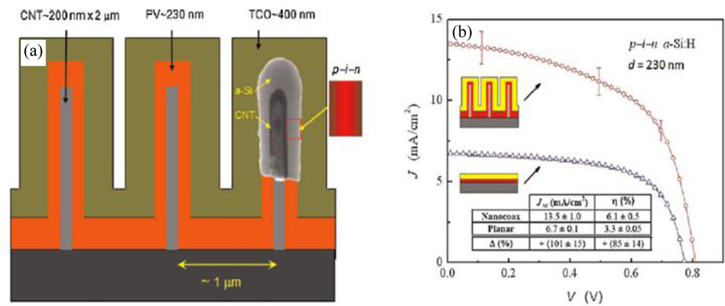
For example, Paudel, et al. fabricated and compared the performance of arrays of coaxial PV cells comprised of Ag-CNT/(n-i-p) a-Si /ITO layers of total diameter ~1 µm on glass substrates with planar cells of the same a-Si thickness and prepared using the same fabrication process as in the coaxial cell.29 As shown in Figure 15, short circuit current density (Jsc) and overall power conversion efficiency (η) gains of ~100% and ~85%, respectively, were achieved on coaxial structures over the planar counterpart. This was accounted for by the enhancement of carrier collection efficiency and light absorption of the coax structures.
Fig. 15.
(a) Schematic of the nanocoax solar cell, and (b) comparison of current–voltage characteristic and performance of nanocoax and planar solar cells under AM1.5 illumination. In the schematic diagram of the coax, CNT means Ag coated CNT and insets are (inside) TEM image of the coax and (right) p-i-n junction sequence. In current–voltage characteristic inset schematics are (top) nanocoax solar cell, (bottom) planar solar cell. Inset table compares the performance of the two solar cell architectures. Reproduced with permission from Ref. 29.
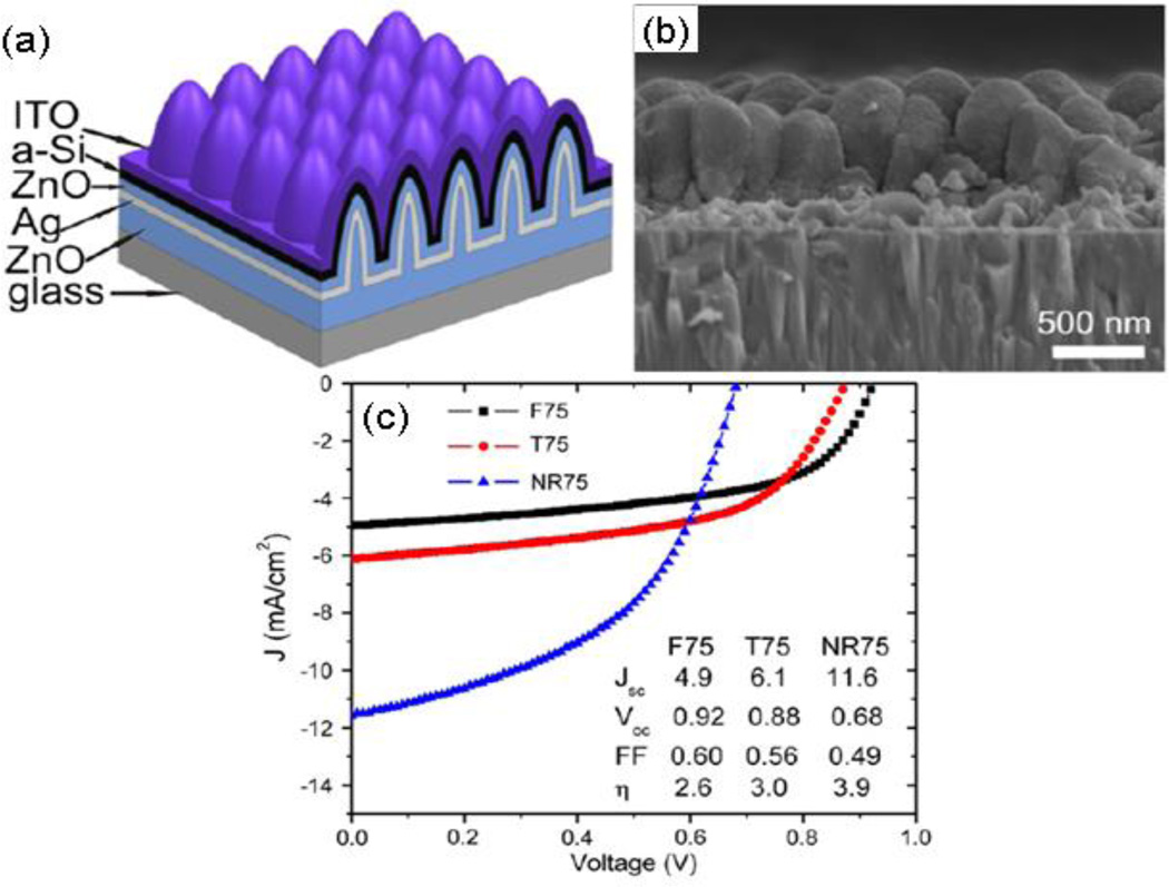
Zhou, et al. reported a similar device as having Jsc and η relative gain of ~25% on a coaxial-like structure over its planar counterpart, but with an initial energy conversion efficiency of less than 1% for coax devices.27 Beside CNTs, ZnO nanocolumns or nanorods were explored as an alternative core to make coaxial solar cells.94,96–98 Vanecek, et al. proposed arrays of nanocoax-like solar cells based on arrays of vertically aligned ZnO nanocolumns, but also reported that it was conceptually simple but experimentally challenging to fabricate a thin functional junction on the vertical side wall of high aspect ratio nanostructures.98 Around the same time, Kuang, et al. employed arrays of ZnO nanorods of average diameter ~110 nm and height 400 nm with areal density 108/cm2 to make arrays of Ag−ZnO−a-Si−ITO coaxial solar cells, as shown in Figure 16. They reported efficiencies of 3.6% and 3.9% for 25 nm and 75 nm thick intrinsic a-Si i-layers, respectively.96,97
Fig. 16.
ZnO-nanorod/a-Si:H solar cell with a 75 nm thick i-layer. (a) Schematic diagram (not to scale) and (b) SEM cross-section view of a completed nanorod/nanocoax solar cell. (c) Comparison of current–voltage characteristic and performance of solar cells with i-layer thickness 75 nm fabricated on planar (F75), texture (T75) and nanorod (NR75) structures. The legend shows the cell parameters. Reproduced with permission from Ref. 97.
Even though the vertical, nanostructure-based coaxial geometry offers clear advantages in terms of carrier collection, light trapping and efficiency, there were drawbacks associated with non-uniformities of the PV and metal coatings. For example, the thickness of the a-Si layer on the sidewall of the vertical structures in Ref. 27 was almost half or one third of thickness on the planar region. This coating conformality of a-Si was improved by changing the geometrical profile of the nanostructure from vertical to conical structures.28,31 Influences of the morphology of the starting template on the conformality of the a-Si coating and efficiency of the solar cell have been studied using different nanostructures. For example, using arrays of glass nanocones as a template, researchers were shown a coaxially structured nanodome a-Si solar cell with 280 nm thick a-Si and of efficiency 5.9%, which corresponds to a 25% relative efficiency enhancement compared to that of the planar control device.99 They performed a systematic study to compare absorption of light and obtained a significantly higher absorption on nanocoax (95%) than planar (65%) devices.
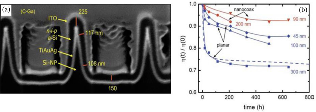
Naughton, et al.28 optimized structures of arrays of nanopillars to minimize the difficulties in the conformal coating and used the pillars as a template to build a nanocoax solar cell as shown in Figure 17. In their research, they metalized arrays of Si nanopillars, then conformally coated n-i-p layers of a-Si of average i layer thickness of ~90 nm, followed by ITO to make a solar cell with 8.2% initial efficiency and 8.4% active area efficiency, which represented ~40% and ~50% improvements, respectively, over the conversion efficiencies of the previously mentioned nanodome and planar solar cells presented in this study.
Fig. 17.
SEM images of a cross-section of a completed n–i–p a-Si nanocoaxial solar cell with average i-layer thickness ~90 nm. Supporting C-Ga was deposited later to enable FIB sectioning. (b) Light-induced degradation of representative planar and nanocoaxial cells with various PV thicknesses. Dashed line is Wronski’s result for a conventional planar a-Si solar cell. Reproduced with permission from Ref. 28.
They also investigated how the nanocoaxial geometry leads to a strong reduction in the Staebler-Wronski light-induced degradation effect100, as shown in Figure 17, where a 90 nm thick nanocoax cell was degraded only ~8% after 500 h, a degradation half or less than of 100 nm and even 45 nm thick planar controls. This reduction of the Staebler-Wronski effect in the coaxial geometry was attributed to a reduction of the absorber layer thickness and the local intensity per unit volume of the incident light. Recently, Hsu, et al. performed a comparative study of the influence of the morphology of a 3D architecture on both the optical and electrical cell performance.101 They used three representative feature shapes on a quartz crystal: vertical nanopillars, convex nanodomes, and concave nanocones, as shown in Figure 18. The concave nanocone designed with ~290 nm thick absorber layer demonstrated the best performance, with initial conversion efficiency of 9.7% as a result of deemed appropriate balance between optical and electric properties. Figure 18 shows SEM images and the current–voltage characteristics of the different structured solar cells measured at AM1.5 illumination. Note, however, the significant voltage and filling factor reductions with the nanopillar and nanodome configurations.
Fig. 18.
(a) Schematics of coaxial solar cell using different nanostructures and SEM images of corresponding cross sections made by FIB milling. (b) Current-voltage characteristics of the nanocoaxial solar cells fabricated from different shaped templates. Reproduced with permission from Ref. 101.
The nonuniform thickness and cracks in the absorber layer were said to be responsible for these reductions. Concurrently, Kim, et al. used the low aspect ratio array of nanocones to make coaxial solar cells with ~150 nm thick a-Si with efficiency 7.6%.31
The coaxial geometry has been used not only for inorganic but also for organic-polymer and dye sensitized solar cells (DSC), as this geometry provides a large surface area for adsorption of light-harvesting molecules simultaneous to the short diffusion length for the charge carriers. Kassegne, et al. used orgacon, a solution-processable highly conductive transparent polymer, to coat an array of SU-8 nanopillars and make orgacon/P3HT(poly(3-hexylthiophene))-PCBM (phenyl-C61-butyric acid methyl ester)/Al coaxial structure solar cells with initial power conversion efficiency of 6.42%, which was ~2.5 times greater than that of the planar control.32 It is important to note that the use of the 3D coaxial geometry provides the self–organized, interpenetrated, nanoscale P3HT:PCBM network with a large donor/acceptor interface area and facilitates exciton separation, thereby improving the overall performance of the devices. However, an optimized device, after tuning different parameters such as array material, diameter, length and pitch, has not yet been reported. More recently, Sun, et al. used the coaxial geometry to increase efficiency and applications of DSCs,30,33,102,103 reporting cell efficiencies between 2.6 and 3.5%.
The nanocoax-based solar cell may thus become a platform for the design of a highly efficient solar cell, by reducing the quantity and quality of the required semiconductor material. However, further efforts will be needed for large-scale fabrication of nanocoax arrays with uniform thickness layers of semiconductors and metals at low cost and with high throughput.
(3.2) Energy Storage Devices
Energy storage devices such as batteries and supercapacitors have been used in many applications, ranging from hybrid electric vehicles and large industrial equipment to handheld electronic devices. Expanding these applications to scale will require light and small volume devices with high energy and power densities. The use of different nanoarchitectures for the miniaturization of the energy storage devices has become a way to create such high energy and power density devices. A synergistic combination of materials and length scales is thus a promising strategy to improve energy storage devices.40,104–107 In this context, nanocoax architectures have been of significant interest. For example, the structures have been used to make high capacitance capacitors because the geometrical structure optimizes the required thickness of the dielectric. High power is one of the important features of conventional electrostatic capacitors. However, it is limited as far as energy storage capacity because energy stored in electrostatic capacitors depends on surface charge density rather than volume charge density. The use of closely-packed, high aspect ratio nanocoaxial structures, on the other hand, promises both high energy and high power density. Banerjee, et al.36 fabricated hexagonally packed, nanocoaxially-structured arrays of TiN-Al2O3-TiN electrostatic capacitors with capacitance up to ~100 µF/cm2, which had higher power (~1×10⁶ W/kg) and energy density (~0.7 W-h/kg) than any other38,108–111 reported electrostatic capacitors to date. The breakdown field of the coaxial capacitor was almost independent of the height of the capacitor, yet much lower than the value for trench capacitors.112 Other similarly structured electrostatic capacitors, such as C-BN-C,38 CNT-Al2O3-CNT,110 and Pt-Al2O3/TiOx-Pt113, have been examined.
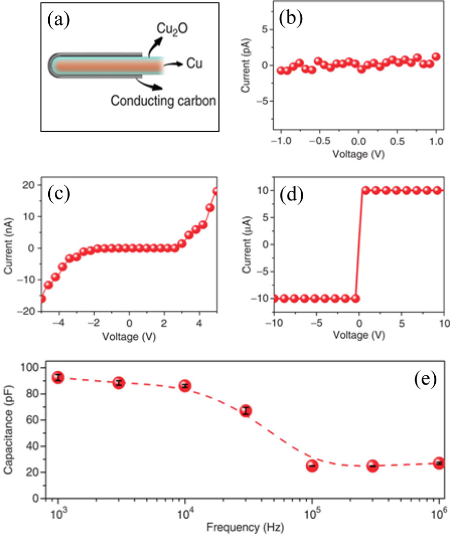
More recently, without using any template method, a single Cu-Cu2O-C coaxial capacitor (Figure 19) with very high value of measured capacitance, ~140 µF/cm2, was reported.37 That measured capacitance was 40 times larger than the value calculated using a classic cylindrical capacitor model. The device also had ~40% higher capacitance per unit area than the highest reported value for a coaxial electrostatic capacitor to date. The authors also studied the I–V characteristics of the Cu-Cu2O-C capacitor for different voltage ranges, as shown in Figure 19.
Fig. 19.
(a) Schematic of Cu-Cu2O-C coaxial nanocapacitor with diameter of inner electrode Cu ~ 90 nm, thickness of dielectric Cu2O ~10 nm and outer metal C ~25 nm. I–V curves for voltage and frequency response of the nanocapacitor. (b) Voltage less than 1 V. (c) Voltage from − 5 to 5 V. (d) The device is permanently broken down by applying a 10 V voltage. (e) Frequency response of the device, solid circles and dotted line were the measured and calculated capacitance between graphitic layer and copper core. Reproduced with permission from Ref. 37.
For applied voltage of less than 1 V, there was no current through the devices, while for voltage of 5 V there was recoverable electrical breakdown, and for applied voltage of 10 V, devices would break down permanently. Based on I-V measurements, the estimated value of the dielectric field strength of the cuprous oxide was more than 100 MVm−1, close to the value for Teflon,114 a widely used insulating material in, e.g. coaxial cables. In addition, such a device has a very high value of capacitance over a wide range of frequencies. This higher value of the capacitance in the frequency response via impedance spectroscopy measurements, compared to that predicated by classical electrostatics, was thought to be due to roughness and a quantum phenomenon associated with a thin film of dielectric of a capacitor.115 Unlike a bulk dielectric, a dielectric layer only a few nanometers thick between two metals does not completely screen an applied electric field between the metals. This phenomenon manifests itself as two quantum capacitors (one for each interface) in series with classical capacitors, yielding the measured capacitance of the capacitor as the equivalent effect of all these capacitors. Moreover, the calculated negative values of quantum capacitance at oxide interfaces explained the remarkably high measured value of the capacitance of the capacitor. Even though the nanocoaxial electrostatic capacitors have excellent thermal stability and high power thresholds, the gravimetric capacitance of the nanocapacitors is less than that of conventional supercapacitors.
Supercapacitors, also called electrochemical capacitors, have two types: EDL and pseudo. They store energy by ion adsorption and fast surface redox reactions, respectively. The use of the coaxial geometry increases both area for adsorption of ions and the frequency of collision of ions on the surface of the electrodes, which could enhance the performance of such devices. Though flexible coaxial microscale supercapacitors have been reported116,117 recently, practical realization of a nanoscale coaxial supercapacitor has not yet been reported.
Based on the above discussion, it is evident that nanocoaxial structure could be key to the creation of an enhanced performance capacitor. However, energy density, or the amount of energy a supercapacitor can store per unit weight, remains very small when compared to batteries. Additionally, the cost of supercapacitor materials often exceeds the cost of battery materials, due to the increased difficulty of creating high-performance supercapacitor materials, such as graphene. Currently, the battery remains the dominant energy storage device (particularly the lithium-ion battery because of its desirable characteristics of high energy density, long cycling life, and high operating voltage). A Li-ion battery converts a chemical potential into electric energy via faradic reaction at the interface of the electrode and electrolyte. These reactions are accompanied by mass and charge transfer. Therefore, the surface area and migration distance are critical parameters to alter the overall electrochemical performance of the devices.40
As in many other fields, the implementation of nanocoaxial electrodes has led to great advances in Li-ion battery performance, such as increased effect of faradic reactions, insertion and extraction kinetics of the ions, avoidance of the deformation of electrodes, combination of materials with high stability and capacity and presence of a case to hold the active materials.57,118,119 For example, Chen, et al. found increased electrochemical performance of the lithium storage material SnO2 in CNT-SnO2-Au coaxial structures, when compared to CNT-SnO2 hetrostructures.57 The poor material cyclability of SnO2 due to the loss of electric contact at the anode, caused by induced stress on the material due to large change in the volume of the material during charging and discharging, was improved by designing the coaxial structure. They found a smaller degree of hysteresis in CNT-SnO2-Au than in CNT-SnO2 electrodes due to improved reversibility of the electrode. Even after many charging and discharging cycles (~40), the discharge capacity of the nanocoax structure was higher than for the heterostructure. These results were attributed to the better reversibility of the insertion and extraction of Li-ions and strong electrical conductivity of the SnO2 layer in the CNT-SnO2-Au structure. Similar CNT-Si-CNT structures made within AAO templates were found to increase the reversibility of a Si anode.120 TEM images of the CNT-Si interface and other electrochemical measurements showed the improvement of the electric contact between CNT and Si layers in the coaxial structure. Although cost effective, large-scale production methods of the coaxial anode have not yet been reported. Nonetheless, the use of a coaxial structured anode is an effective way to simultaneously improve the electrochemical specific capacity, cyclic performance, and stability of the rechargeable Li-ion batteries.
(3.3) Electronic Devices
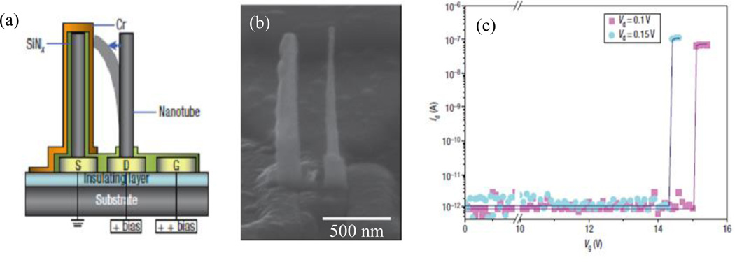
Some of the unique physical properties that arise from the nanocoaxial structure offer great opportunities to make nanoscale electronic devices. The nanocoax geometry can expand the capabilities of capacitive memory devices. Jang, et al.48 reported nanoelectromechanical (NEM) memory devices having source, drain, and gate as shown in Figure 20(a).
Fig. 20.
(a) Schematic of a NEM memory device. Source S is connected to ground, and the drain D and gate G are connected to the bit line and the word line, respectively, to receive electrical signals. The coaxial capacitors on source has nanotubes (grey) of diameter ~60 nm, the dielectric layer (green) and metal layer (orange) of thickness ~40 nm and ~30 nm respectively. The applied positive bias voltage deflects the nanotube on the drain to make contact and charged the capacitor. On removal of the gate bias voltage, the nanotube returns to its original position and leaves the coaxial capacitor in a charged state. (b) SEM image of fabricated device in (c) The current between the source and drain, Id, as a function of Vg, the voltage between the gate and drain, for two values of Vd, the voltage between the drain and the source (with the source electrode connected to ground). Below a threshold gate voltage, Id is effectively zero. This is the ‘OFF’ state of the NEM device. Above the threshold voltage nanotube makes contact with the capacitor, which allows current to flow between the drain and the source. This is the ‘ON’ state of the NEM devices. Reproduced with permission from Ref. 48.
In this device, a mechanically-active CNT was used as a drain and a coaxial (CNT-SiNx-Cr) structure as a source to form a memory cell. In operation, the source was electrically connected to ground, the drain was connected to the bit line, to which a constant positive voltage was applied, and the gate was connected to the word line. By adjusting the height of the CNT, the source-drain and drain-gate separations, and the gate potential, the coaxial capacitor can become charged. This was used as a bit of stored information. Above a threshold voltage, small changes in the bias voltage sharply switched the drain current between ON and OFF states, as shown in Figure 20. These devices were free from the complicated processing steps present in the formation of p-n junctions and had small leakage current compared to Si-based devices. However, the fabrication process did have various technical obstacles, specifically in the growth of the CNT.
(3.4) Sensing Devices
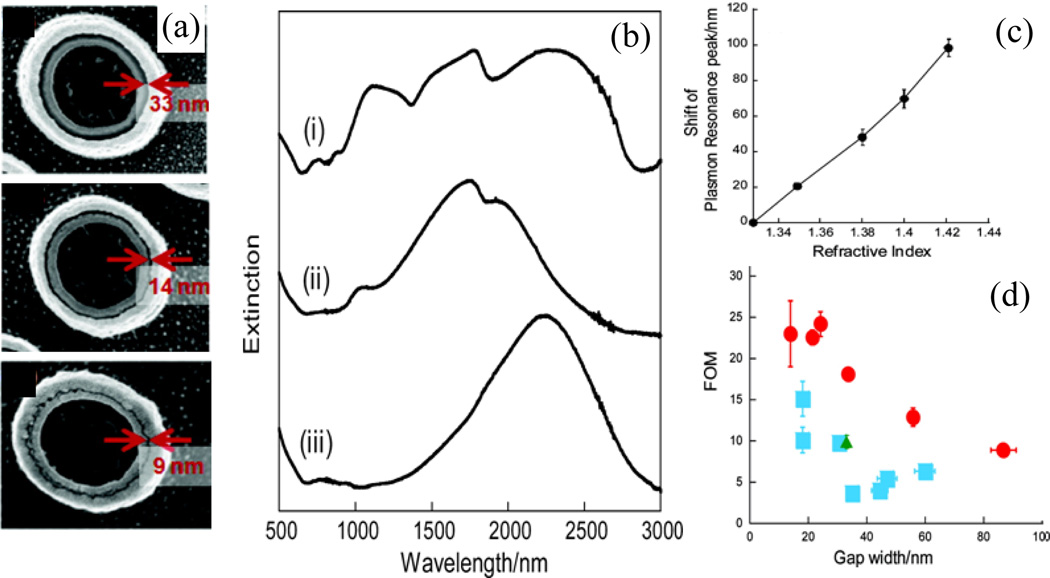
Nanocoax structures have been used to achieve different types of transduction, such as optical, electrical impedance, and electrochemical, for the detection of chemical and biological molecules. For example, Hao, et al. performed theoretical studies of coaxial (concentric) and non-coaxial (non-concentric) plasmonic structures designed from a Au disk and ring for the possibility of localized surface plasmon resonance (LSPR)-based refractive index sensing.121 They found that the values at which peaks occur in the spectra of both structures were strongly affected by changes in refractive index in the gap region between the disk and the ring, resulting in the coaxial structure being a strong candidate for a plasmonic sensor. However, in both partially and fully filled cavities, the sensitivity of the non-coaxial structure was higher than that of the coaxial structure, which was gauged for broken symmetry of the structure. The use of LSPR was further explored by Kubo, et al., who used coaxially-structured Au “double nanopillar” (i.e. nanocoax) arrays with different sized nanogaps.44 They evaluated the effect of the coaxial structure’s annulus width on the performance of plasmonic sensor. As in Figure 21, some resonance peaks in the structure were due to plasmon hybridization and were proposed to be of two origins: a symmetric dipole mode of the inner pillar and quadrupole mode of the outer pillar. These resonance peak positions depended on the coupling strength and energy of plasmon in the inner and outer pillars of the coax, which were sensitive to the surrounding medium of the coax and were shifted according to the change in the refractive index of the surrounding medium.
Fig. 21.
(a) SEM images of nanocoax with various nanogap annulus. (b) Extinction spectra in air of (i) nanocoax with 33 nm gap annulus, (ii) inner Au nanopillar, and (iii) outer Au nanopillar. (c) Relationship between plasmon resonance shift and environmental refractive indices. Plasmon resonance peak shifted to longer wavelength region depends linearly with the refractive indices. (d) Correlation between annulus gap width of nanocoax and FOM value. Red circles, cyan squares, are from nanocoax with hollowed and TiO2 annulus, where as green triangle was from combination of inner and outer nanopillars. Error bars of x- and y-axes represent standard errors of nanogap width and FOM value. Reproduced with permission from Ref. 44.
Moreover, the enhanced electromagnetic field strength in the gap between the two pillars made the coaxial structure a strong candidate for a plasmonic sensor. The performance of coaxial plasmonic sensors was tested by examining the shift in the peak of the extinction spectrum of the coax with hollow and partially filled annuli, which were immersed in deuteron water and ethylene glycol solutions, as shown in Figure 21. It is important to note that there was not a significant shift in peak values with the gap between pillars. However, the sensitivity expressed in terms of a figure of merit (FOM) was altered by the volume of cavity available for solution, as shown in Figure 21.
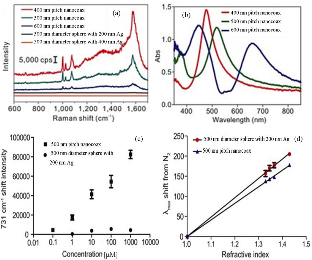
Im, et al. used the arrays of nanocoax made using arrays nanosphere for LSPR and surface-enhanced Raman scattering/spectroscopy (SERS) biosensing.69 In this work, SERS signals from benzenethiol (1 mM) coated nanocoaxes arrays of 400, 500 and 600 nm pitches due to excitation wavelength of 514.5 nm were reported with all nanocoaxes yielding at least 10-fold higher Raman intensity than 500 nm diameter metalized (i.e. Agcoated) nanospheres. The enhancement in the nanocoaxial structure may have been due conversion of integrated light inside the nanospheres into plasmons, which could ultimately produce enhanced electromagnetic fields in the cavity annulus of the nanocoax and hence in the SERS signal. As shown in Figure 22(a) for the given excitation wavelength, SERS signals from different arrays of nanocoaxes have different enhancement factors. This could be due to different positions of the resonance peaks in the LSPR spectra for nanocoax arrays with different pitches, as shown in Figure 22(b).
Fig. 22.
(a) Raman spectra for benzenethiol from arrays of nanocoaxes of 400, 500 and 600 nm pitches illuminated by 514.5 nm wavelength excitation. The spectra form arrays of 500 nm diameter sphere coated by 200 and 400 nm Ag were also presented. (b) LSPR spectra from benzenethiol coated nanocoax arrays of different pitches. (c) The intensities of SERES signals at 735 cm−1 shift form arrays of 500 nm pitch nanocoax and 500 nm diameter metalized sphere exposed with different concentrations of adenine. Both arrays were illuminated by 532 nm wavelength laser. (d) Shift in LSPR vs. refractive index of surrounding media of arrays of nanocoax and nanosphere of 500 nm pitch and diameter, respectively. Reproduced with permission from Ref. 69.
The nanocoax array with 400 nm pitch and the highest enhancement in SERS signal has its resonance position closest to the excitation wavelength 514.5 nm. Similarly, for 532 nm excitation wavelength, 500 nm pitch nanocoax arrays produced the highest enhancement in SERS signal. These results indicate that the maximum SERS enhancement can be obtained by changing the size of nanospheres to match the corresponding excitation wavelength. Figure 22(c) shows the sensing performance of nanocoaxes and metalized nanospheres based SERS sensors for the detection of adenine, a commonly detected molecule in DNA sensing experiments. The reported limit of detection of adenine solution in water in the nanocoax,76 nM, was about order of magnitude smaller than with the nanospheres (524 nM). In addition to SERS-based sensing, these authors employed arrays of nanocoaxes and metalized nanospheres to make LSPR-based sensors. As shown in Figure 22(d) for bulk solvents, metalized nanospheres showed slightly higher sensitivity (~481 nm/RIU) than arrays of nanocoaxes (~412 nm/RIU). Here, RIU refers to refractive index units. However, for surface-bonded molecules, nanocoax-based devices were found to be more sensitive than nanosphere-based devices.
The high enhancement factor in SERS signals and the significant shift in LSPR peak for molecules bound on the surface indicate that the nanocoax array structure may provide a combined platform for highly sensitive SERS and LSPR biosensing.
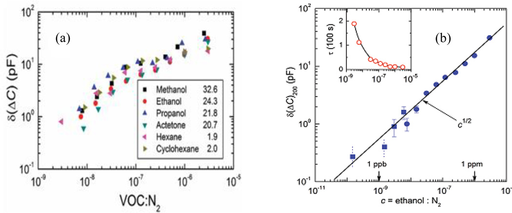
More recently, Zhao, et al. employed arrays of nanocoaxes with a porous Al2O3 dielectric to make a highly sensitive capacitive chemical detector.45 The performance of the device for detection of different concentrations of volatile organic compounds diluted in N2 gas, as well as various humidity levels, was reported with an ultimate sensitivity of sub-part-per-billion for ethanol, corresponding to about 30 ethanol molecules per nanocoax, as shown in Figure 23. However, the device as described has limited chemical specificity.
Fig. 23.
(a) Concentration-dependent response of various volatile organic compounds. Numbers in the legends are the values of relative permittivity εr of the tested chemicals. (b) Performance of the nanocoax sensor for the detection of ethanol diluted in N2 gas, as the average response of the coax after subtraction of the N2 background and recorded 200 s after ethanol application, δ(ΔC)200 versus the concentration of ethanol. Inset: derived time constant for the different concentrations of ethanol. Reproduced with permission from Ref. 45.
It is important to note that in this device, the porosity of the dielectric played a crucial role in the sensor performance. The authors used sputter deposited Al2O3 of porosity ~10%. Moreover, the coaxial sensor had a rapid response of only a few seconds for concentrations above ~100 ppb and ~100 s for ppb-level detection of ethanol. The response at low concentration (ppb) was ~83% more rapid than other reported times for comparable concentration of ethanol using other devices. This suggested that sensitivity and response and recovery time of the device could be improved by using other porous media122 or elevating the working temperature. However, ways to improve the specificity of the device have yet to be explored.
The sensing applications of the nanocoax array device were further extended by making an electrochemical sensor.46 Rizal, et al. compared the performance of an electrochemical sensor (ES) composed of an array of vertically-oriented nanoscale coaxial electrodes, with the coax cores and shields serving as integrated working electrode (WE) and counter electrode (CE), respectively. This is shown in Figure 24(a) and (b), where devices with a nanoscale WE-CE separation gap (coax annulus width) were compared to a planar sensor control, which had conventional millimeter-scale electrode gap spacing.
Fig. 24.
(a) SEM image of an array of partially hollow nanocoaxes of 1.3 µm pitch, 200 nm annulus thickness, and 500 nm annulus depth with Au inner and Cr outer electrodes. Bottom portion shows a cross-section of one row of the array prepared by FIB milling. (b) Schematic of a coax-based ES made using inner and outer electrodes of the coax array as WE and CE , respectively. (c) DPV signal from coax-based ES with 100 to 400 nm gaps between WE and CE, plotted vs. WE potential. ES control (planar) having millimeter-scale WE−CE gap is also shown. (d) Left axis: Difference between peak current and current at 0.1 V WE potential vs. gap (r2−r1) between WE and CE for nanocoax-based ES. Right axis: Ratio of current density in coax-based ES cell to that in planar ES vs. gap between WE and CE of nanocoax-based ES. Reproduced with permission from Ref. 46.
Differential pulse voltammetry (DPV) measurements on 1 mM ferrocene carboxylic acid showed that the coax-based sensor with a 100 nm gap had sensitivity ~100 times greater than that of a planar control. This two-decade improvement in sensitivity was ascribed primarily to the nanogap provided by the coaxial geometry. In the case of the coax-based ES where the width of the coaxial annulus controlled the distance between electrodes, the sensitivity increased as the electrode separation decreased, as shown in Figure 24. However, in practice, it was difficult to exchange liquid completely into and out of the nanogap between the electrodes for the smallest gap devices. Further development of this type of device was suggested to be required in order to improve the liquid exchange in the nanogap.
4) Conclusions
It is clear that nanocoax-based devices can offer advantages in a number of technical applications. Recent research has demonstrated the numerous advances in the development of reliable and economical methods for the preparation of nanocoaxes (and arrays thereof ) from different materials. Although a more sophisticated, template-free method, such as the use of CNTs, is a direct route for the fabrication of arrays of nanocoax, the use of lithographically patterned structures or chemically-synthesized nonporous membranes as templates for nanocoaxes provides a more economical and reproducible way to make arrays of nanocoaxes. Moreover, the use of the conical nanopillar and ALD yield the most conformal coating of different layers of the coaxial structure.
While physical properties of electromagnetic, electronic, and electrochemical nanocoax structures have been studied, there are many more areas of investigation for practical implementations of these structures. For example, transmission of light through subwavelength coaxial waveguides has been demonstrated, yet detailed quantification of the waveguiding properties of subwavelength coaxial waveguides and use of the device for the manipulation of light at subwavelength scale must still be analyzed. The nanocoax structure provides a powerful platform for an efficient solar cell design, yet several major challenges must be overcome for these solar cells to become a viable energy source. The nanocoax geometry indeed plays a unique role in the enhancement of optical absorption, as high optical absorption is a necessary aspect of a solar cell, but is not sufficient to make an efficient solar cell. It should be noted that the huge junction area per unit of projected area and pores on the active layer that originate from inhomogeneous growth of semiconducting materials within the nanocoaxial structure each increase surface recombination, which limits Voc of the solar cell. Therefore, a balance between the optical properties and electrical properties, that is, optically rough and electrically flat, would be desired to enhance the overall performance of a nanocoax solar cell. Creating low aspect ratio structures using surface passivation layers or materials with low surface states could minimize the problem of surface recombination while creating the p-n junction in the nanocoaxial solar cell. Besides energy conversion, the nanocoax structure offers clear advantages in many energy storage applications that continue to be extensively explored. For instance, using arrays of nanocoax structures fabricated on a light-weight flexible substrate as the anode could increase the stability and the energy density of a Li-ion battery. Utilizing the unique properties of the nanocoaxial structure for making miniaturized sensors has been established. Although the high aspect ratio of the nanocoax structure allows for fast diffusion of gaseous analyte molecules through a porous annulus of a coaxial structure, ways for selective adsorption of molecules and rapid recovery of the device must be explored to increase selectivity and response time of the sensor. By functionalizing the surface of the electrode(s) and through integration with microfluidic devices, this nanocoax device could become a notable landmark in the progress of cost effective, portable, sensitive and label-free biosensors.
Additionally, a single nanocoax structure offer unique functions in logic, memory and other applications to improve density and performance of many electronic devices. In particular, a single nanocoaxial transistor and capacitor can be used in a wide variety of electronic circuits. However, a reliable and cost effective process for positioning and interconnection of nanocoaxial structures has to be established to integrate them into electronic circuits.
Supplementary Material
Acknowledgements
This work was supported in part by the National Institutes of Health (National Cancer Institute and National Institute of Allergy and Infectious Diseases) and the W.M. Keck Foundation.
References
- 1.Thomson W. Philos. Mag. Ser. 4. 1855;9:531–535. [Google Scholar]
- 2.Leighton GC, Woodford DR. Am. Teleph. Telegr. Co. 1968;47 [Google Scholar]
- 3.Huang X, Neretina S, El-Sayed MA. Adv. Mater. 2009;21:4880–4910. doi: 10.1002/adma.200802789. [DOI] [PubMed] [Google Scholar]
- 4.Lauhon LJ, Gudiksen MS, Wang D, Lieber CM. Nature. 2002;420:57–61. doi: 10.1038/nature01141. [DOI] [PubMed] [Google Scholar]
- 5.Barth S, Hernandez-Ramirez F, Holmes JD, Romano-Rodriguez A. Prog. Mater. Sci. 2010;55:563–627. [Google Scholar]
- 6.Volder MFLD, Tawfick SH, Baughman RH, Hart AJ. Science. 2013;339:535–539. doi: 10.1126/science.1222453. [DOI] [PubMed] [Google Scholar]
- 7.Mikolajick T, Heinzig A, Trommer J, Pregl S, Grube M, Cuniberti G, Weber WM. Phys. Status Solidi RRL - Rapid Res. Lett. 2013;7:793–799. [Google Scholar]
- 8.Zhang C, Yan Y, Zhao YS, Yao J. Annu. Rep. Sect. C Phys. Chem. 2013;109:211–239. [Google Scholar]
- 9.Suenaga K, Colliex C, Demoncy N, Loiseau A, Pascard H, Willaime F. Science. 1997;278:653–655. [Google Scholar]
- 10.Baida FI, Van Labeke D. Phys. Rev. B. 2003;67:155314. [Google Scholar]
- 11.Porto JA, García-Vidal FJ, Pendry JB. Phys. Rev. Lett. 1999;83:2845–2848. [Google Scholar]
- 12.Catrysse PB, Fan S. Appl. Phys. Lett. 2009;94:231111. [Google Scholar]
- 13.Ebbesen TW, Lezec HJ, Ghaemi HF, Thio T, Wolff PA. Nature. 1998;391:667–669. [Google Scholar]
- 14.Wang Y, Plummer EW, Kempa K. Adv. Phys. 2011;60:799–898. [Google Scholar]
- 15.Rybczynski J, Kempa K, Herczynski A, Wang Y, Naughton MJ, Ren ZF, Huang ZP, Cai D, Giersig M. Appl. Phys. Lett. 2007;90:021104. [Google Scholar]
- 16.Saleh AAE, Dionne JA. Nano Lett. 2012;12:5581–5586. doi: 10.1021/nl302627c. [DOI] [PubMed] [Google Scholar]
- 17.Melli M, Polyakov A, Gargas D, Huynh C, Scipioni L, Bao W, Ogletree DF, Schuck PJ, Cabrini S, Weber-Bargioni A. Nano Lett. 2013;13:2687–2691. doi: 10.1021/nl400844a. [DOI] [PubMed] [Google Scholar]
- 18.Merlo JM, Ye F, Rizal B, Burns MJ, Naughton MJ. Opt. Express. 2014;22:14148–14154. doi: 10.1364/OE.22.014148. [DOI] [PubMed] [Google Scholar]
- 19.Lim KP, Lee CW, Singh G, Wang Q. J. Nanophotonics. 2013;7:070598–070598. [Google Scholar]
- 20.Ndao A, Belkhir A, Salut R, Baida FI. Appl. Phys. Lett. 2013;103:211901. [Google Scholar]
- 21.Burgos SP, de Waele R, Polman A, Atwater HA. Nat. Mater. 2010;9:407–412. doi: 10.1038/nmat2747. [DOI] [PubMed] [Google Scholar]
- 22.Iwanaga M, Ikeda N, Sugimoto Y. Phys. Rev. B. 2012;85:045427. [Google Scholar]
- 23.de Waele R, Burgos SP, Polman A, Atwater HA. Nano Lett. 2009;9:2832–2837. doi: 10.1021/nl900597z. [DOI] [PubMed] [Google Scholar]
- 24.Weber-Bargioni A, Schwartzberg A, Cornaglia M, Ismach A, Urban JJ, Pang Y, Gordon R, Bokor J, Salmeron MB, Ogletree DF, Ashby P, Cabrini S, Schuck PJ. Nano Lett. 2011;11:1201–1207. doi: 10.1021/nl104163m. [DOI] [PubMed] [Google Scholar]
- 25.Camacho RE, Morgan AR, Flores MC, McLeod TA, Kumsomboone VS, Mordecai BJ, Bhattacharjea R, Tong W, Wagner BK, Flicker JD, Turano SP, Ready WJ. JOM. 2007;59:39–42. [Google Scholar]
- 26.Zhang Y, Wang, Mascarenhas A. Nano Lett. 2007;7:1264–1269. doi: 10.1021/nl070174f. [DOI] [PubMed] [Google Scholar]
- 27.Zhou H, Colli A, Ahnood A, Yang Y, Rupesinghe N, Butler T, Haneef I, Hiralal P, Nathan A, Amaratunga GAJ. Adv. Mater. 2009;21:3919–3923. [Google Scholar]
- 28.Naughton MJ, Kempa K, Ren ZF, Gao Y, Rybczynski J, Argenti N, Gao W, Wang Y, Peng Y, Naughton JR, McMahon G, Paudel T, Lan YC, Burns MJ, Shepard A, Clary M, Ballif C, Haug F-J, Söderström T, Cubero O, Eminian C. Phys. Status Solidi RRL - Rapid Res. Lett. 2010;4:181–183. [Google Scholar]
- 29.Paudel T, Rybczynski J, Gao YT, Lan YC, Peng Y, Kempa K, Naughton MJ, Ren ZF. Phys. Status Solidi A. 2011;208:924–927. [Google Scholar]
- 30.Weintraub B, Wei Y, Wang ZL. Angew. Chem. Int. Ed. 2009;48:8981–8985. doi: 10.1002/anie.200904492. [DOI] [PubMed] [Google Scholar]
- 31.Kim J, Hong AJ, Nah J-W, Shin B, Ross FM, Sadana DK. ACS Nano. 2012;6:265–271. doi: 10.1021/nn203536x. [DOI] [PubMed] [Google Scholar]
- 32.Kassegne S, Moon K, Martín-Ramos P, Majzoub M, Őzturk G, Desai K, Parikh M, Nguyen B, Khosla A, Chamorro-Posada P. J. Micromechanics Microengineering. 2012;22:115015. [Google Scholar]
- 33.Sun H, Li H, You X, Yang Z, Deng J, Qiu L, Peng H. J. Mater. Chem. A. 2013;2:345–349. [Google Scholar]
- 34.Naughton MJ. 8,588,920. U.S. Patent. 2013
- 35.Naughton MJ, Kempa K, Ren Z. 7,623,746. U.S. Patent. 2009
- 36.Banerjee P, Perez I, Henn-Lecordier L, Lee SB, Rubloff GW. Nat. Nanotechnol. 2009;4:292–296. doi: 10.1038/nnano.2009.37. [DOI] [PubMed] [Google Scholar]
- 37.Liu Z, Zhan Y, Shi G, Moldovan S, Gharbi M, Song L, Ma L, Gao W, Huang J, Vajtai R, Banhart F, Sharma P, Lou J, Ajayan PM. Nat. Commun. 2012;3:879. doi: 10.1038/ncomms1833. [DOI] [PubMed] [Google Scholar]
- 38.Shelimov KB, Davydov DN, Moskovits M. Appl. Phys. Lett. 2000;77:1722–1724. [Google Scholar]
- 39.Frackowiak E. Phys. Chem. Chem. Phys. 2007;9:1774–1785. doi: 10.1039/b618139m. [DOI] [PubMed] [Google Scholar]
- 40.Bruce PG, Scrosati B, Tarascon J-M. Angew. Chem. Int. Ed. 2008;47:2930–2946. doi: 10.1002/anie.200702505. [DOI] [PubMed] [Google Scholar]
- 41.Shen G, Chen P-C, Ryu K, Zhou C. J. Mater. Chem. 2009;19:828–839. [Google Scholar]
- 42.Penner RM. Annu. Rev. Anal. Chem. 2012;5:461–485. doi: 10.1146/annurev-anchem-062011-143007. [DOI] [PubMed] [Google Scholar]
- 43.Li J, Lu Y, Ye Q, Cinke M, Han J, Meyyappan M. Nano Lett. 2003;3:929–933. [Google Scholar]
- 44.Kubo W, Fujikawa S. Nano Lett. 2011;11:8–15. doi: 10.1021/nl100787b. [DOI] [PubMed] [Google Scholar]
- 45.Zhao H, Rizal B, McMahon G, Wang H, Dhakal P, Kirkpatrick T, Ren Z, Chiles TC, Naughton MJ, Cai D. ACS Nano. 2012;6:3171–3178. doi: 10.1021/nn205036e. [DOI] [PubMed] [Google Scholar]
- 46.Rizal B, Archibald MM, Connolly T, Shepard S, Burns MJ, Chiles TC, Naughton MJ. Anal. Chem. 2013;85:10040–10044. doi: 10.1021/ac402441x. [DOI] [PubMed] [Google Scholar]
- 47.Park YK, Ahn YS, Kim SB, Lee KH, Cho CH, Chung TY, Kim K. J. Korean Phys. Soc. 44:112. [Google Scholar]
- 48.Jang JE, Cha SN, Choi YJ, Kang DJ, Butler TP, Hasko DG, Jung JE, Kim JM, Amaratunga GAJ. Nat. Nanotechnol. 2008;3:26–30. doi: 10.1038/nnano.2007.417. [DOI] [PubMed] [Google Scholar]
- 49.Brown KA, Satzinger KJ, Westervelt RM. Nanotechnology. 2012;23:115703. doi: 10.1088/0957-4484/23/11/115703. [DOI] [PubMed] [Google Scholar]
- 50.Hyun JK, Zhang S, Lauhon LJ. Annu. Rev. Mater. Res. 2013;43:451–479. [Google Scholar]
- 51.Tian B, Kempa TJ, Lieber CM. Chem. Soc. Rev. 2008;38:16–24. doi: 10.1039/b718703n. [DOI] [PubMed] [Google Scholar]
- 52.Kwong D-L, Li X, Sun Y, Ramanathan G, Chen ZX, Wong SM, Li Y, Shen NS, Buddharaju K, Yu YH, Lee SJ, Singh N, Lo GQ. J. Nanotechnol. 2011;2012:e492121. [Google Scholar]
- 53.Mieszawska AJ, Jalilian R, Sumanasekera GU, Zamborini FP. Small Weinh. Bergstr. Ger. 2007;3:722–756. doi: 10.1002/smll.200600727. [DOI] [PubMed] [Google Scholar]
- 54.Xia Y, Yang P, Sun Y, Wu Y, Mayers B, Gates B, Yin Y, Kim F, Yan H. Adv. Mater. 2003;15:353–389. [Google Scholar]
- 55.Yin L-W, Bando Y, Zhu Y-C, Li M-S, Tang CC, Golberg D. Adv. Mater. 2005;17:213–217. [Google Scholar]
- 56.Guo S, Dong S, Wang E. Small. 2008;4:1133–1138. doi: 10.1002/smll.200800094. [DOI] [PubMed] [Google Scholar]
- 57.Chen G, Wang Z, Xia D. Chem. Mater. 2008;20:6951–6956. [Google Scholar]
- 58.Chen Y, Lin Wang Z, Song Yin J, Johnson DJ, Prince RH. Chem. Phys. Lett. 1997;272:178–182. [Google Scholar]
- 59.Fan W, Zhang S, Malloy KJ, Brueck SRJ. Opt. Express. 2005;13:4406. doi: 10.1364/opex.13.004406. [DOI] [PubMed] [Google Scholar]
- 60.Fan W, Zhang S, Minhas B, Malloy K, Brueck S. Phys. Rev. Lett. 2005;94:033902. doi: 10.1103/PhysRevLett.94.033902. [DOI] [PubMed] [Google Scholar]
- 61.Chen X, Park H-R, Pelton M, Piao X, Lindquist NC, Im H, Kim YJ, Ahn JS, Ahn KJ, Park N, Kim D-S, Oh S-H. Nat. Commun. 2013;4:2361. doi: 10.1038/ncomms3361. [DOI] [PubMed] [Google Scholar]
- 62.Im H, Bantz KC, Lindquist NC, Haynes CL, Oh S-H. Nano Lett. 2010;10:2231–2236. doi: 10.1021/nl1012085. [DOI] [PubMed] [Google Scholar]
- 63.Yang H, Lightner CR, Dong L. ACS Nano. 2012;6:622–628. doi: 10.1021/nn204055t. [DOI] [PubMed] [Google Scholar]
- 64.Chen H, Wang N, Di J, Zhao Y, Song Y, Jiang L. Langmuir ACS J. Surf. Colloids. 2010;26:11291–11296. doi: 10.1021/la100611f. [DOI] [PubMed] [Google Scholar]
- 65.Diggle JW, Downie TC, Goulding CW. Chem. Rev. 1969;69:365–405. [Google Scholar]
- 66.Xia Y, Whitesides GM. Annu. Rev. Mater. Sci. 1998;28:153–184. [Google Scholar]
- 67.Lipomi DJ, Kats MA, Kim P, Kang SH, Aizenberg J, Capasso F, Whitesides GM. ACS Nano. 2010;4:4017–4026. doi: 10.1021/nn100993t. [DOI] [PubMed] [Google Scholar]
- 68.Rizal B, Ye F, Dhakal P, Chiles TC, Shepard S, McMahon G, Burns MJ, Naughton MJ. In: Nano-Optics for Enhancing Light-Matter Interactions on a Molecular Scale. Bartolo BD, Collins J, editors. Netherlands: Springer; 2013. pp. 359–370. [Google Scholar]
- 69.Im H, Bantz KC, Lee SH, Johnson TW, Haynes CL, Oh S-H. Adv. Mater. 2013;25:2678–2685. doi: 10.1002/adma.201204283. [DOI] [PubMed] [Google Scholar]
- 70.Carny O, Shalev DE, Gazit E. Nano Lett. 2006;6:1594–1597. doi: 10.1021/nl060468l. [DOI] [PubMed] [Google Scholar]
- 71.Baida FI, Labeke DV, Granet G, Moreau A, Belkhir A. Appl. Phys. B. 2004;79:1–8. [Google Scholar]
- 72.Baida FI. Appl. Phys. B. 2007;89:145–149. [Google Scholar]
- 73.Baida FI, Belkhir A, Arar O, Barakat EH, Dahdah J, Chemrouk C, Van Labeke D, Diebold C, Perry N, Bernal M-P. Micron Oxf. Engl. 1993;2010(41):742–745. doi: 10.1016/j.micron.2010.06.009. [DOI] [PubMed] [Google Scholar]
- 74.Lawrence N, Dal Negro L. Frontiers in Optics 2010/Laser Science XXVI. Optical Society of America; 2010. FThC7. [Google Scholar]
- 75.de Waele R, Burgos SP, Atwater HA, Polman A. Opt. Express. 2010;18:12770–12778. doi: 10.1364/OE.18.012770. [DOI] [PubMed] [Google Scholar]
- 76.Roberts A. Opt. Express. 2010;18:2528–2533. doi: 10.1364/OE.18.002528. [DOI] [PubMed] [Google Scholar]
- 77.Baida FI, Belkhir A, Van Labeke D, Lamrous O. Phys. Rev. B. 2006;74:205419. [Google Scholar]
- 78.Poujet Y, Roussey M, Salvi J, Baida FI, Van Labeke D, Perentes A, Santschi C, Hoffmann P. Photonics Nanostructures - Fundam. Appl. 2006;4:47–53. [Google Scholar]
- 79.Peng Y, Wang X, Kempa K. Opt. Express. 2008;16:1758–1763. doi: 10.1364/oe.16.001758. [DOI] [PubMed] [Google Scholar]
- 80.Kempa K, Wang X, Ren ZF, Naughton MJ. Appl. Phys. Lett. 2008;92:043114. [Google Scholar]
- 81.Kozina O, Nefedov I, Melnikov L, Karilainen A. Materials. 2010;4:104–116. doi: 10.3390/ma4010104. [DOI] [PMC free article] [PubMed] [Google Scholar]
- 82.Ahnood A, Zhou H, Dai Q, Vygranenko Y, Suzuki Y, Esmaeili-Rad M, Amaratunga G, Nathan A. Nano Lett. 2013;13:4131–4136. doi: 10.1021/nl401636v. [DOI] [PubMed] [Google Scholar]
- 83.Chapin DM, Fuller CS, Pearson GL. J. Appl. Phys. 1954;25:676–677. [Google Scholar]
- 84.Green MA. Prog. Photovolt. Res. Appl. 2006;14:383–392. [Google Scholar]
- 85.Carlson DE, Wronski CR. Appl. Phys. Lett. 1976;28:671–673. [Google Scholar]
- 86.Yamamoto K, Yoshimi M, Tawada Y, Okamoto Y, Nakajima A, Igari S. Appl. Phys. A. 1999;69:179–185. [Google Scholar]
- 87.Britt J, Ferekides C. Appl. Phys. Lett. 1993;62:2851–2852. [Google Scholar]
- 88.Siddiki MK, Li J, Galipeau D, Qiao Q. Energy Environ. Sci. 2010;3:867–883. [Google Scholar]
- 89.Lewis NS. Science. 2007;315:798–801. doi: 10.1126/science.1137014. [DOI] [PubMed] [Google Scholar]
- 90.Tsakalakos L, Balch J, Fronheiser J, Korevaar BA, Sulima O, Rand J. Appl. Phys. Lett. 2007;91:233117. [Google Scholar]
- 91.Tu W-C, Chang Y-T, Yang C-H, Yeh D-J, Ho C-I, Hsueh C-Y, Lee S-C. Appl. Phys. Lett. 2010;97:193109. [Google Scholar]
- 92.Lu Y, Lal A. Nano Lett. 2010;10:4651–4656. doi: 10.1021/nl102867a. [DOI] [PubMed] [Google Scholar]
- 93.Huynh WU, Dittmer JJ, Alivisatos AP. Science. 2002;295:2425–2427. doi: 10.1126/science.1069156. [DOI] [PubMed] [Google Scholar]
- 94.Kuang Y, Vece MD, Rath JK, van Dijk L, Schropp REI. Rep. Prog. Phys. 2013;76:106502. doi: 10.1088/0034-4885/76/10/106502. [DOI] [PubMed] [Google Scholar]
- 95.Kayes BM, Atwater HA, Lewis NS. J. Appl. Phys. 2005;97:114302. [Google Scholar]
- 96.Kuang Y, van der Werf KHM, Houweling ZS, Schropp REI. Appl. Phys. Lett. 2011;98:113111. [Google Scholar]
- 97.Kuang Y, van der Werf KHM, Houweling ZS, Di Vece M, Schropp REI. J. Non-Cryst. Solids. 2012;358:2209–2213. [Google Scholar]
- 98.Vanecek M, Babchenko O, Purkrt A, Holovsky J, Neykova N, Poruba A, Remes Z, Meier J, Kroll U. Appl. Phys. Lett. 2011;98:163503. [Google Scholar]
- 99.Zhu J, Hsu C-M, Yu Z, Fan S, Cui Y. Nano Lett. 2010;10:1979–1984. doi: 10.1021/nl9034237. [DOI] [PubMed] [Google Scholar]
- 100.Staebler DL, Wronski CR. Appl. Phys. Lett. 1977;31:292–294. [Google Scholar]
- 101.Hsu C-M, Battaglia C, Pahud C, Ruan Z, Haug F-J, Fan S, Ballif C, Cui Y. Adv. Energy Mater. 2012;2:628–633. [Google Scholar]
- 102.Sun H, You X, Yang Z, Deng J, Peng H. J. Mater. Chem. A. 2013;1:12422–12425. [Google Scholar]
- 103.Bae J, Park YJ, Lee M, Cha SN, Choi YJ, Lee CS, Kim JM, Wang ZL. Adv. Mater. 2011;23:3446–3449. doi: 10.1002/adma.201101345. [DOI] [PubMed] [Google Scholar]
- 104.Duay J, Gillette E, Hu J, Lee SB. Phys. Chem. Chem. Phys. 2013;15:7976–7993. doi: 10.1039/c3cp50724f. [DOI] [PubMed] [Google Scholar]
- 105.Aricò AS, Bruce P, Scrosati B, Tarascon J-M, van Schalkwijk W. Nat. Mater. 2005;4:366–377. doi: 10.1038/nmat1368. [DOI] [PubMed] [Google Scholar]
- 106.Wang Y, Cao G. Adv. Mater. 2008;20:2251–2269. [Google Scholar]
- 107.Guo Y-G, Hu J-S, Wan L-J. Adv. Mater. 2008;20:2878–2887. [Google Scholar]
- 108.Roozeboom F, Elfrink R, Verhoeven J, van den Meerakher J, Holthuysen F. Microelectron. Eng. 2000;53:581–584. [Google Scholar]
- 109.Klootwijk JH, Jinesh KB, Dekkers W, Verhoeven JF, Van Den Heuvel FC, Kim H-D, Blin D, Verheijen MA, Weemaes RGR, Kaiser M, Ruigrok J, Roozeboom F. IEEE Electron Device Lett. 2008;29:740–742. [Google Scholar]
- 110.Sohn JI, Kim Y-S, Nam C, Cho BK, Seong T-Y, Lee S. Appl. Phys. Lett. 2005;87:123115. [Google Scholar]
- 111.Kemell M, Ritala M, Leskelä M, Ossei-Wusu E, Carstensen J, Föll H. Microelectron. Eng. 2007;84:313–318. [Google Scholar]
- 112.Banerjee P, Ditali A. IEEE Electron Device Lett. 2004;25:574–576. [Google Scholar]
- 113.Lee G, Lai B-K, Phatak C, Katiyar RS, Auciello O. J. Appl. Phys. 2013;114:027001. [Google Scholar]
- 114.Haynes WM. CRC Handbook of Chemistry and Physics, 94th Edition. 94 th edition. CRC Press; 2013. [Google Scholar]
- 115.Luryi S. Appl. Phys. Lett. 1988;52:501–503. [Google Scholar]
- 116.Le VT, Kim H, Ghosh A, Kim J, Chang J, Vu QA, Pham DT, Lee J-H, Kim S-W, Lee YH. ACS Nano. 2013;7:5940–5947. doi: 10.1021/nn4016345. [DOI] [PubMed] [Google Scholar]
- 117.Zhang Z, Chen X, Chen P, Guan G, Qiu L, Lin H, Yang Z, Bai W, Luo Y, Peng H. Adv. Mater. 2014;26:466–470. doi: 10.1002/adma.201302951. [DOI] [PubMed] [Google Scholar]
- 118.Liao J-Y, Higgins D, Lui G, Chabot V, Xiao X, Chen Z. Nano Lett. 2013;13:5467–5473. doi: 10.1021/nl4030159. [DOI] [PubMed] [Google Scholar]
- 119.Li Z, Yuan L, Yi Z, Liu Y, Xin Y, Zhang Z, Huang Y. Nanoscale. 2014;6:1653–1660. doi: 10.1039/c3nr04347a. [DOI] [PubMed] [Google Scholar]
- 120.Zhao C, Li Q, Wan W, Li J, Li J, Zhou H, Xu D. J. Mater. Chem. 2012;22:12193–12197. [Google Scholar]
- 121.Hao F, Nordlander P, Sonnefraud Y, Dorpe PV, Maier SA. ACS Nano. 2009;3:643–652. doi: 10.1021/nn900012r. [DOI] [PubMed] [Google Scholar]
- 122.Broom DP, Thomas KM. MRS Bull. 2013;38:412–421. [Google Scholar]
Associated Data
This section collects any data citations, data availability statements, or supplementary materials included in this article.


