Abstract
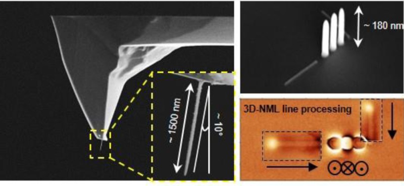
Nanomagnet logic (NML) is a relatively new computation technology that uses arrays of shape-controlled nanomagnets to enable digital processing. Currently, conventional resist-based lithographic processes limit the design of NML circuitry to planar nanostructures with homogeneous thicknesses. Here, we demonstrate the focused electron beam induced deposition of Fe-based nanomaterial for magnetic in-plane nanowires and out-of-plane nanopillars. Three-dimensional (3D) NML was achieved based on the magnetic coupling between nanowires and nanopillars in a 3D array. Additionally, the same Fe-based nanomaterial was used to produce tilt-corrected high-aspect-ratio probes for the accurate magnetic force microscopy (MFM) analysis of the fabricated 3D NML gate arrays. The interpretation of the MFM measurements was supported by magnetic simulations using the Object Oriented MicroMagnetic Framework. Introducing vertical out-of-plane nanopillars not only increases the packing density of 3D NML but also introduces an extra magnetic degree of freedom, offering a new approach to input/output and processing functionalities in nanomagnetic computing.
Keywords: nanomagnet logic, electron beam induced deposition, iron, magnetic nanowires, nanomagnetism, MFM, computational nanotechnology
Introduction
Nanomagnet logic (NML) is a promising future computational technology combining data storage and processing using magnetic phenomena.1 The advantages of NML, such as nonvolatility, ultralow power dissipation, and CMOS compatibility, are fundamental for modern logic devices.2,3 In NML, magnetic nanowires (NWs) encode the Boolean values “0” and “1” in their bistable magnetization directions, while digital processing is based on magnetic coupling among adjacent structures.4 This technology is under continuous development, covering both device integration and nanostructure optimization aspects. For the improvement of NML key-elements, many efforts have been devoted to planar two-dimensional (2D) designs by introducing slanted edges5,6 or sharp extremities7 or by merging NWs in curved nanostructures8 for the magnetic key-element improvement. In all these nanostructures, the magnetization vector is confined to the substrate plane, and only some works have reported on NML key-elements magnetized out-of-plane (OP).9−12 This is due to the fact that most of the nanofabrication techniques used until now are based on multistep processes, which typically lead to in-plane (IP) magnetic nanostructures with uniform height.4,13,14
In our previous work,8 we demonstrated how focused electron beam induced deposition (FEBID) allows synthesis of nanostructures of magnetic materials with tuned height avoiding the use of masks, resists, and the consequent liftoff process. FEBID is a chemical vapor deposition process promoted by a focused electron beam that locally decomposes a gas precursor, leading to nanometer-sized deposits.15 Moreover, this nanofabrication technique allows the deposition of any nanostructure geometry from zero-dimensional (0D) to three-dimensional (3D).16−18 FEBID deposits, particularly those based on Fe and Co have been successfully used for several applications in the field of nanomagnetism19,20 such as magnetic nanoprobes21 and nano-Hall-22 and magnetologic devices.8,23 For example, Franken et al. recently demonstrated how OP-nanopillars (NP) can be used as pinning sites for magnetic domain wall.24
In this work, we demonstrate the first ever deposition of combined Fe-based IP-NW and OP-NP arrays for 3D-NML computing. In addition, a novel way of imaging the magnetic properties of such arrays has been developed. Magnetic force microscopy (MFM) imaging of nanostructures with very high aspect ratios is not feasible with commercially available probes due to the significant topographic artifacts, caused by the shape of the tip. Therefore, conventional pyramidal AFM tips have been modified by FEBID in order to obtain high-aspect-ratio, tilt-compensated MFM probes. The FEBID-modified probes developed here helped minimizing the influence of the sample topography in the MFM measurements. Furthermore, the magnetization states of isolated NPs and 3D-NML arrays have been simulated using the Object Oriented MicroMagnetic Framework (OOMMF) software.25 These simulations enabled a more accurate interpretation of the MFM results and supported the functionality of the 3D logic systems theoretically. In the future, NML technology based on 3D arrays facilitates increased packing density because the OP elongated nanomagnets have a smaller footprint than that of IP high-aspect-ratio structures. Furthermore, in 3D-NML a third possible magnetization direction is introduced by the OP geometry. Hence, 3D-NML exhibits an extra magnetic degree of freedom, which could allow for separation of digital processing from input/output functionality, for example.
Discussion
Crystallinity and Composition of FEBID Fe-based Nanopillars
FEBID of Fe-rich magnetic nanostructures was performed with an Fe(CO)5 precursor. In Figure 1a, a sketch of the FEBID process is shown together with SEM micrographs of the main structures realized in this work, that is, the vertical nanostructures deposited on AFM probes (Figure 1b) and on bulk Si (Figure 1c). For clarity, from here on, we refer to the structures deposited on the AFM probes as needles, and those deposited on bulk Si as NPs. Figure 1b,c demonstrates the two main advantages of the FEBID approach: (1) the capability of fabricating nanostructures on an arbitrary substrate and (2) the fabrication of structures of any geometry with excellent thickness control. The height of the FEBID deposits has been tuned varying the deposition time, where, for example, longer electron beam exposure led to higher deposits. The magnetic properties of both nanosystems are strongly influenced by their chemical composition and crystallinity. Therefore, an extensive study of these properties was required. Here, the needles and NPs were assumed to have analogous chemistry and crystallinity because they were deposited in the same way, and hence the following considerations are assumed to be valid for all OP structures obtained in this work.
Figure 1.
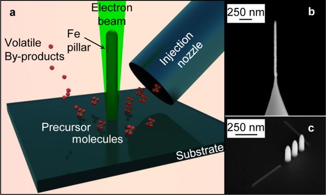
(a) Illustration of the focused electron beam induced deposition of vertical Fe structures. The precursor is injected in proximity of an electron beam that locally promotes the decomposition of the precursor molecules. (b) SEM micrographs of an Fe needle deposited on a commercial AFM tip. This demonstrates the capability of FEBID to deposit on arbitrary substrates. (c) SEM micrograph of a 3D-NML digital line transport array based on IP and OP nanostructures.
Figure 2a shows a TEM micrograph of a needle deposited on a commercial Si AFM probe with a 10 s exposure time. The needle’s height is about 1200 nm and it has an approximate width of 55 nm. Elemental mapping executed by energy filtered TEM (EFTEM, Figure 2b), revealed that the needle consisted of an inner iron core covered by a thin (∼5 nm) oxide shell. C is homogeneously distributed throughout the whole needle, whereas the small particle on the needle tip is assumed to be incorporated during the sample handling. A thin Si layer was present on one side of the needle due to redeposition during the ion beam milling of the cantilever. In addition, the chemical composition of the center region was investigated by electron energy loss spectrometry (EELS), revealing a high Fe content (∼75%), with smaller fractions of O (∼15%) and C (∼10%). However, such analyses probed a cross section of the needle, and therefore, the O content in the core is likely overestimated, given the oxide shell layer observed covering the needle. This implies that the Fe content in the needle core is higher than 75%. The high Fe content, in turn, gives rise to the ferromagnetic properties of the needles and NPs.
Figure 2.
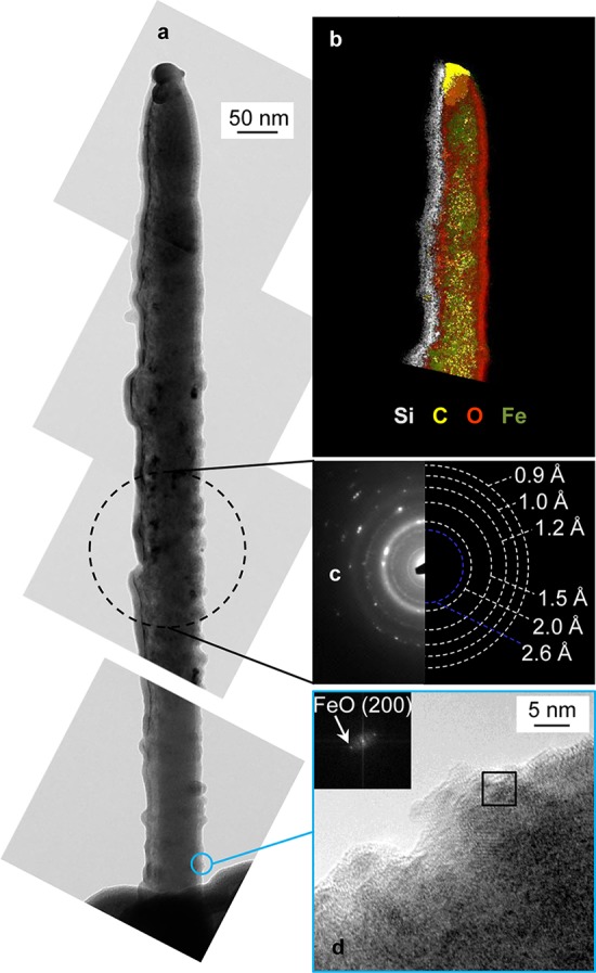
TEM analyses of an Fe needle deposited on a commercial AFM tip. (a) TEM micrographs displaying an overview of the Fe needle along its height. (b) EFTEM elemental mapping of the needle tip. The Fe core is covered by a thin oxide layer (∼5 nm), while C is distributed throughout the whole structure. The presence of Si on the side of the needle is due to redeposition from the FIB-milling during the sample preparation. (c) Diffraction pattern of the needle, which mainly shows α-Fe and bcc-FeO polycrystalline phases (white dashed lines). Traces of fcc-Fe3O4 (blue dashed line) are also present. (d) HR-TEM micrograph showing that the thin oxide layer mainly consists of FeO.
The crystallinity of the needle was investigated by selected area electron diffraction (SAED), performed at different positions along the needle’s height (Supplementary Figure S1, Supporting Information). A typical SAED pattern (Figure 3c) revealed α-Fe (ferrite) and bcc-FeO as the main phases, with traces of fcc-Fe3O4. In particular, the high-resolution TEM micrograph (Figure 2d) indicated that the oxide shell layer was mainly composed of bcc-FeO. The results from the composition and crystallinity studies presented here are in good agreement with corresponding results obtained in previous studies of IP NWs and 2D nanostructures.8,16 The low crystallinity of the FEBID nanostructures can be assumed to strongly affect their magnetic properties. In particular, the magnetic anisotropy is likely dominated by shape anisotropy, and the contribution from magneto-crystalline anisotropy can be assumed to be very small due to the lack of texturing.26
Figure 3.
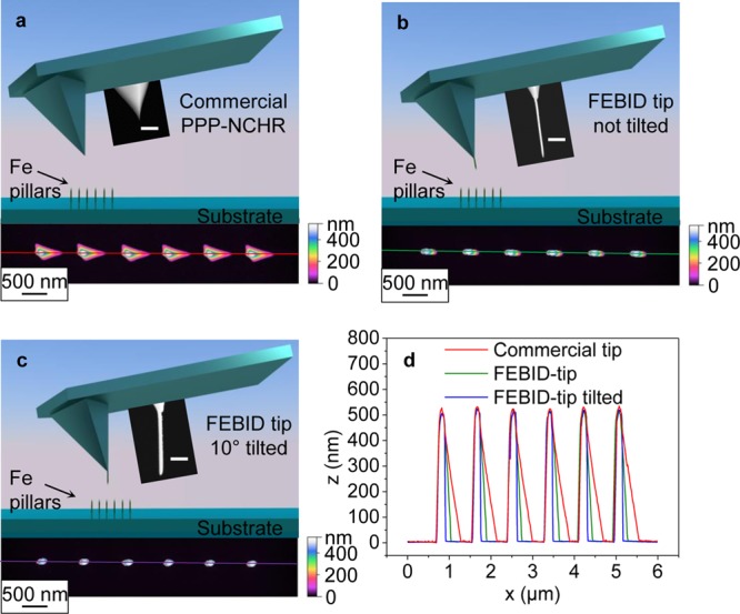
Responses of different AFM probes for investigation of OP high-aspect-ratio structures. (a–c) Different probe geometries used for AFM analyses of free-standing NPs. The SEM micrograph (scale bar = 300 nm) in panel a shows the geometry at the apex of the probe. Furthermore, below each sketch, the AFM height images of 550 nm high NPs obtained using the different probes are shown. (d) AFM cross section of the NPs using the (red) commercial, (green) FEBID modified, and (blue) FEBID modified tilt-corrected probe.
The Importance of Using High-Aspect-Ratio, Tilt-Corrected MFM Probes
Among all experimental techniques available for investigating small magnetic nanostructures, MFM stands out due to its noninvasive and high-resolution performance. However, OP high-aspect-ratio structures are particularly challenging to investigate using conventional MFM probes. The typical geometry of commercially available AFM probes is pyramidal (Figure 3a). Along the front edge of the tip, the half angle is nominally 25°, while at the back edge of the tip, the half angle is approximately 10°. Considering that the cantilever is mounted with a 10° tilt with respect to the substrate, the actual front and back edge half angles will be 35° and 0°, respectively. Moreover, additional topography artifacts in the AFM image will arise due to the lateral sides of the pyramid, which are characterized by identical half cone angles of about 17°. To reduce the artifacts caused by the commercial tip geometry and to properly image the OP structures of this work, we modified commercial AFM probes by FEBID. Figure 3b shows an SEM micrograph of such a modified FEBID needle, with a height and width of ∼1280 and ∼50 nm, respectively. Similar MFM probes made of Co have already been demonstrated in previous works.21,27 However, novel to the work presented here was compensating the tilt of the FEBID needle, to accommodate the 10° tilt of the mounted cantilever, thus minimizing the artifacts on all sides of the imaged nanostructures. To achieve this, we performed the FEBID synthesis after tilting the sample stage and, consequently, the cantilever by 10°. Here too, the exposure time was 10 s, making the needle ∼1350 nm long and ∼55 nm wide (Figure 3b).
Figure 3d shows three AFM profiles of ∼520 nm high NPs deposited for 3 s each obtained with a commercial, FEBID-modified, tilt-compensated probe. The results clearly demonstrate that it is only possible to obtain proper AFM and, consequently, MFM images of 3D-NML key-elements by using the new magnetic, high-aspect ratio and tilt-corrected probes. The geometry of the FEBID deposits is characterized by a main structure surrounded by a thin layer called a “halo”. This unique geometry is caused by the different electron-solid interactions of the primary electron beam with the substrate. The inelastic scattering of the primary electrons (PEs) with the substrate’s atoms produces the so-called secondary electrons 1 (SE1s). SE1s typically have energies in the 5–50 eV range and are responsible for the deposition of the main structure.15,28 Elastic scattering of the PEs in the substrate lead to so-called back scattered electrons (BSEs). The BSEs are reflected back to the surface from a wider area than the beam diameter with comparable energy to the PEs. These BSEs are themselves producing secondary electrons 2 (SE2s) by inelastic collisions, which are responsible for the formation of the halo layer.29 Another contribution to the growth of the halo layer originates from electrons produced by scattering of PEs on the freshly grown main structure, the so-called forward scattered electrons (FSEs).30,31
Figure 4 shows an MFM image of FEBID Fe NPs, deposited for 1 s. In MFM, the magnetization of the tip is directed perpendicular to the sample surface, and the regions having magnetization components OP lead to a change in contrast in the phase shift image. In Figure 4 the average NP height estimated from AFM was ∼180 nm, while the average diameter was estimated to be ∼70 nm using SEM (Supplementary Figure S2, Supporting Information). Such structures can be assumed to exhibit strong shape anisotropy, where the major (easy) and minor (hard) axes are oriented OP and IP, respectively. Hence, the NPs are expected to exhibit a single domain magnetic configuration, where the magnetization vector points either inward or outward with respect to the substrate surface.32,33 The specimen was premagnetized in a magnetic field of ∼1.80 kOe applied IP, that is, along the NPs’ hard axis. Consequently, after field removal, it is expected that the magnetization direction in an isolated NP can point either up or down with the same probability. Each NP in the MFM image is characterized by a ∼50 nm wide area slightly shifted to the left side of the NP and enclosed in a large circular region with opposite contrast extending over 250 nm around the main structure (Figure 4b). The contrast in the small inner region indicates the magnetization orientation of the NP with respect to that of the tip, that is, bright and dark contrasts correspond to repulsive and attractive interactions, respectively. In our case, the tip magnetization is known, and dark and bright contrasts correspond to magnetization directions pointing outward and inward, respectively. In addition, the MFM phase shift shows a circular region with opposite contrast surrounding the center of the NPs.
Figure 4.
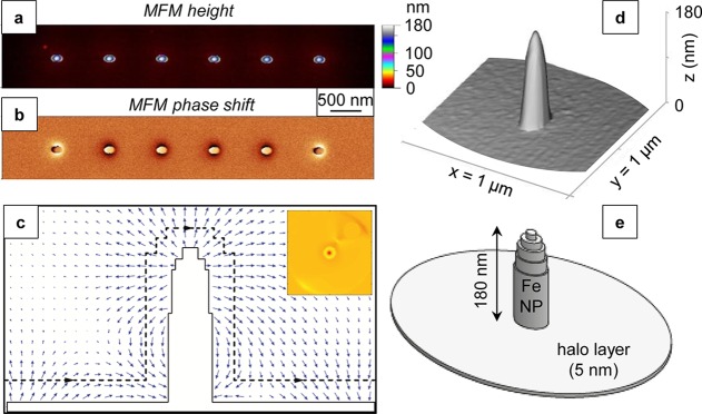
(a) Height and (b) phase shift MFM images of an array of six NPs deposited by FEBID. The 1 μm spacing between neighboring NPs excluded any magnetic interactions. (c) Cross-sectional OOMMF simulation of a single NP showing the (blue arrows) magnetic stray field, (black dashed line) the track of a virtual MFM probe in lift mode, and (inset) the corresponding MFM phase shift image obtained from OOMMF simulations. (d) 3D MFM height image of a NP and (e) the model used for the OOMMF simulations.
To give a correct description of the circular region, we performed OOMMF simulations, considering the peculiar geometry of the NPs. The same simulation settings as those used in our previous work16 were employed, except for the magneto-crystalline anisotropy, which was set to zero, assuming the grain size of the deposits to be smaller than the dimensions of a typical domain wall.26 A 3D AFM image and the 3D model used for the OOMMF simulations are shown in Figure 4, panels d and e, respectively. The OOMMF simulation in Figure 4c shows the magnetic stray field emitted from a NP. Furthermore, the dashed black line indicates a simulated track of a virtual MFM probe scanned at a constant lift height of 20 nm from the NP (Figure 4c). The calculated MFM response from this scan revealed a phase shift image analogous to the experimental ones, in which a central zone is surrounded by a circular region with opposite contrast. According to the simulations, such a change in contrast indicates a change in orientation of the magnetic stray field surrounding the NP. However, in the measured MFM phase shift, the central contrast is shifted to the left side of the NP. This shift is most likely due to the uncertainty on the tilt compensation of the probe. Furthermore, to investigate the influence of the halo layer on these observations, we varied the MS of the halo between 0 and 1700 kA/m in the simulations. It was found that the halo did not influence the magnetization of the NP but did have a smoothing effect on the contrast in the simulated MFM image. However, if such an effect exists in the MFM measurements as well, is not possible to verify from the present investigations. The material analysis of the TEM investigation suggests that the halo consists mainly of FeO with traces of Fe3O4, assuming it has similar properties as the oxide shell observed covering the NPs. Hence, the halo should only have a limited effect on the magnetization of the NPs. Still, Serrano-Ramón et al.34 have shown that even an oxidized halo can influence the magnetic properties. To further understand the influence of the halo layer, Nikulina et al.35 and De Teresa et al.36 proposed its removal via ion milling. However, such an investigation goes beyond the scope of this study, in which it is presently not experimentally possible to isolate the influence of the halo on the magnetic properties of the NPs from other effects. Hence, a detailed investigation of the effect of the halo on high aspect ratio NPs deposited by FEBID is left to future work. However, it is important to point out that the simulations suggested that the halo should only have a limited effect on the NPs and should not be strong enough to affect the orientation of their magnetization.
3D NML Computing
The system discussed so far was based on isolated NPs (>1 μm spacing) like those shown in Figure 4a. However, in order to achieve 3D-NML, IP-NWs and OP-NPs have been deposited very close to each other, enabling the magnetic coupling between neighboring structures to process the digital information. The MFM analysis in Figure 5a, demonstrates the functionality of digital line transport, where horizontal “input” (i-NW) and vertical “output” (o-NW) NWs were separated by three NPs deposited along a line. Both NWs were 440 nm long and 40 nm wide, while the three NPs were 180 nm high and 70 nm wide (Supplementary Figure S2, Supporting Information). The sample was premagnetized using an electromagnet with a magnetic field strength of ∼1.80 kOe applied in the direction shown by the white arrow in Figure 5a. Such a magnetic field, called a “clocking field” (Hclock), induced the NPs and o-NW in an intermediate magnetic state where their magnetization pointed along their hard axes. The magnetization state of the i-NW, on the other hand, was set along its easy axis. Subsequently, after Hclock removal, the i-NW magnetic fringe fields determined the ground-state configuration of the whole array. The alternating contrast in the phase shift MFM image (Figure 5a) demonstrates an antiferromagnetic coupling between NPs. Finally, the magnetization state of the o-NW was determined by the magnetic fringing field of the closest NP.
Figure 5.
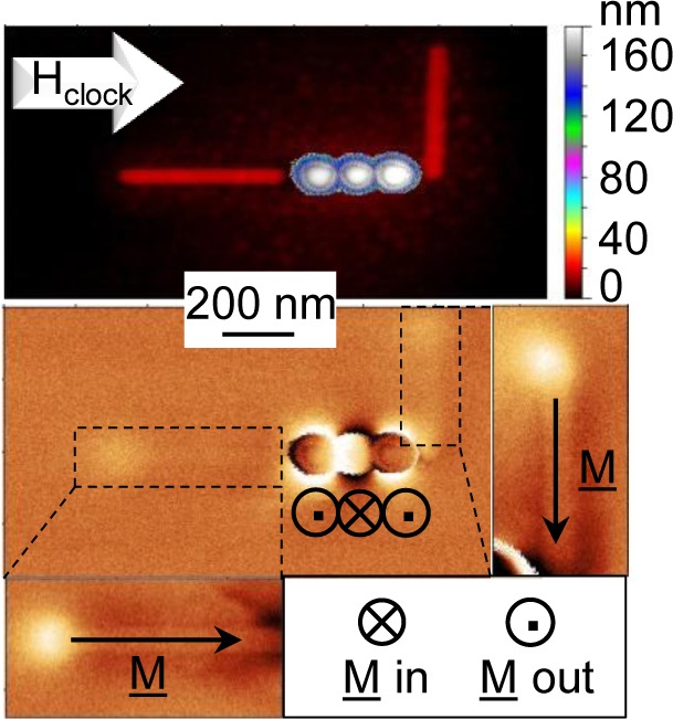
(Top) Topographical and (bottom) phase shift images of a FEBID line processing array. The white arrows in the topographical image indicate the direction of the applied clock field. The magnetization directions (M) at remanence are shown by the black arrows for the IP-NW, and the symbols shown in the inset describe the orientation of the OP-NPs.
The FEBID process allowed separating the input/output and processing nanoelements of 3D-logic arrays in two different planes. However, proper functionality of the 3D digital line gate was heavily dependent on strength and, more importantly, the alignment of Hclock with respect to the FEBID array, which was limited to ±3° of accuracy in our experimental setup. This issue was also observed in the OOMMF simulations, which indicated that a misalignment of Hclock of only a few degrees (∼2–3°) was enough to switch the magnetization in the o-NW in the direction of the misalignment. Hence, a small misalignment of Hclock had a stronger effect on the magnetization of the o-NW than did the fringe field of the NP array. Consequently, a stronger magnetic coupling between NPs and NWs was required to achieve a reliable 3D-logic array.
As a successful solution to this problem, we propose to unify IP and OP nanomagnets in one single nanostructure (NS), by FEBID of a NP directly on top of the end of a NW. Here, this strategy was used in a new design of a 3D-NML majority gate array, composed of three novel NSs and two NPs (Supplementary Figure S3, Supporting Information). In the new array, the three NSs are used as inputs (i-NS), where their NPs are introduced in an array with two additional NPs without NWs. The five NPs are oriented in a cross geometry, where the NPs of the NSs enclose a central NP (c-NP) on three sides.
A fifth output NP (o-NP) is positioned on the forth arm of the cross (Figure 6). An MFM investigation of this new majority gate design is shown in Figure 6a, where the magnetostatic coupling of the three i-NS determined the orientation of the magnetization vector of the c-NP. The c-NP is, in turn, magnetically coupled to the o-NP, determining its magnetic configuration. The MFM measurements on this new gate design correlated well with the OOMMF simulations, in which similar pillar orientation was observed, as can be seen in Figure 6, where the AFM, MFM, and OOMMF investigations of such a gate are shown. The orientation of the magnetization of the NPs was independent of the MS of the halo, and remained the same if the halo was completely removed. However, the magnetization orientation in the simulations was sensitive to small (∼5%) changes in the geometrical and magnetic properties of the array, for example, NP diameter and MS. This indicates that the precision and reproducibility of the FEBID deposition process is fundamental for the reliability of NML arrays. Similar observations were made in the MFM investigation, in which the yield of the majority gate deposition was about 63% (Supplementary Figure S4, Supporting Information).
Figure 6.
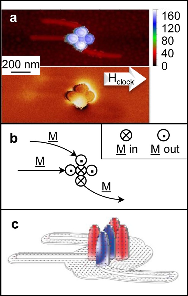
3D-NML majority gate prototype of merged IP and OP nanostructures. (a) MFM investigation of the 3D array based on merged IP-NWs and OP-NPs. On one end of three inputs IP-NWs, an OP-NP has been deposited. The magnetic configuration of these three OP nanostructures is governed by the magnetization of the IP-NWs. The three input NPs are magnetically coupled to a central NP which, in turn, is magnetically coupled to the output NP. The magnetic resolution in the MFM phase shift image is limited by the relatively high lift height (∼80 nm), chosen to minimize the topography-induced artifacts. (b) The direction of the magnetization vectors in the array. (c) OOMMF simulation after Hclock removal, illustrating the orientation of the magnetization of the NPs in the 3D-NML majority gate prototype. This configuration was independent of the MS of the halo when varied between 0 and 1700 kA/m.
Conclusions
In this work, FEBID was used as a direct write technique for the synthesis of NML gates composed of IP- and OP-nanostructures magnetically coupled with each other. The magnetization configuration of the obtained 3D-NML arrays was investigated by MFM. This investigation was made possible by a novel FEBID-modified magnetic, high-aspect-ratio MFM probe. Fe needles with a height-to-width aspect ratio of ∼25:1 were fabricated on commercial AFM tips. Furthermore, a 10° tip tilt-correction was introduced to minimize tip artifacts in the AFM/MFM images. Magnetic OOMMF simulations were employed to correctly interpret the MFM phase shift images of isolated NPs, giving the necessary insight into the magnetic interactions between the NPs and the MFM probe. All nanosystems realized in this work were fabricated by FEBID in a single-step process in which nanostructures with different heights were deposited within the same process step. This exceptional capability of FEBID, combined with the absence of masks or resists, make this deposition technique the perfect candidate for rapid prototyping of 3D-NML technology. Furthermore, we have demonstrated the functionality of digital processing using IP and OP nanostructures. Particularly, the transfer of digital information via magnetic coupling from IP to OP nanostructures and vice versa was shown to be feasible. We believe that 3D-NML concept not only increases the circuit packing density due to the NPs small radius but also allows to separate data processing and input/output units in two different planes, increasing the control over these systems. Furthermore, a new 3D-NML majority gate design comprising united IP-NW and OP-NP was also realized. The simulated orientation of the magnetizations of the NPs in the array correlated well with the magnetic configuration revealed by MFM. We believe that this new design will further increase the circuit packing density in NML circuitry and reduce computational errors due to unstable magnetic coupling.
Methods
Iron-rich NWs and NPs have been synthesized at room temperature by FEBID, using iron pentacarbonyl (Fe(CO)5) as gas precursor. The support material Si(100) was precleaned via ultrasonication in acetone and isopropanol. The deposition was performed in a Zeiss Leo1530VP scanning electron microscope equipped with a self-built gas injection system, originally described by Hochleitner et al.37 The instrument base pressure was ∼2.0 × 10⁻⁶ mbar, and the pressure during the precursor injection was ∼3.0 × 10⁻⁵ mbar. In order to obtain IP-NWs, the electron beam was guided with high precision by a Raith ELPHY Plus pattern generator; acceleration voltages and beam current were 3 kV and 1.0 nA. The point pitch was 5 nm with a dwell time of 204.8 μs. The total exposure time of each NW was ∼0.6 s. Pillar deposition was executed by scanning a single spot with a dwell time of 500 ms. The total exposure times for isolated NPs and the 3D-NML array were 3 and 1 s, respectively. FEBID magnetic and tilt-compensated needles were synthesized on commercial PPP-NCHR AFM probes using the LEO-32 V04.00.10 software in spot mode. The total spot exposure time was 10 s. The tip angle compensation was achieved by tilting the stage 10° (±2°). Morphological, structural, and compositional TEM characterizations were performed using an FEI Tecnai F20-FEG transmission electron microscope equipped with a GATAN Tridiem energy filter. For the elemental maps in Figure 2b, the three-window method was applied to the Fe–L, O–K, and C–K edge at 708, 532, and 284 eV energy loss, respectively. The magnetic investigations of NPs and NWs synthesized on Si(100) substrate were carried out on a commercial Dimension 3100 atomic force microscope (Veeco/Bruker) using the FEBID-modified probes.
Acknowledgments
The research leading to these results has received funding from the Austrian Science Fund (FWF) under project P24093 and from the European Community’s Seventh Framework Programme (FP7/2007-2013) under grant agreement number ENHANCE-238409. Fabrication of nanostructures was performed at the Center for Micro- and Nanostructures (ZMNS) of the Vienna University of Technology. The authors gratefully acknowledge the support of the Center for Micro- and Nanostructures (ZMNS) at the Vienna University of Technology.
Supporting Information Available
Further TEM crystallinity studies executed on the Fe NPs; SEM and MFM investigations of 3D-NML arrays. This material is available free of charge via the Internet at http://pubs.acs.org.
The authors declare no competing financial interest.
Supplementary Material
References
- Wolf S. A.; Lu J.; Stan M. R.; Chen E.; Treger D. M. The Promise of Nanomagnetics and Spintronics for Future Logic and Universal Memory. Proc. IEEE 2010, 98, 2155–2168. [Google Scholar]
- Niemier M. T.; Bernstein G. H.; Csaba G.; Dingler A.; Hu X. S.; Kurtz S.; Liu S.; Nahas J.; Porod W.; Siddiq M.; Varga E. Nanomagnet Logic: Progress toward System-Level Integration. J. Phys.: Condens. Matter 2011, 23, 0953–8984. [DOI] [PubMed] [Google Scholar]
- Vasil’eva N.; Kasatkin S.; Petrukhin B. Programmable Ferromagnet-Semiconductor Logic Devices. Autom. Remote Control 2004, 65, 1357–1376. [Google Scholar]
- Orlov A.; Imre A.; Csaba G.; Ji L.; Porod W.; Bernstein G. H. Magnetic Quantum-Dot Cellular Automata: Recent Developments and Prospects. J. Nanoelectron. Optoelectron. 2008, 3, 55–68. [Google Scholar]
- Liu S.; Hu X.; Niemier M.; NAHAS J.; Csaba G.; Bernstein G.; Porod W. Exploring the Design of the Magnetic-Electrical Interface for Nanomagnet Logic. IEEE Trans. Nanotechnol. 2013, 11, 220–230. [Google Scholar]
- Niemier M. T.; Varga E.; Bernstein G. H.; Porod W.; Alam M. T.; Dingler A.; Orlov A.; Hu X. S. Shape Engineering for Controlled Switching With Nanomagnet Logic. IEEE Trans. Nanotechnol. 2012, 11, 220–230. [Google Scholar]
- Dey H.; Csaba G.; Hu X. S.; Niemier M.; Bernstein G. H.; Porod W. Switching Behavior of Sharply Pointed Nanomagnets for Logic Applications. IEEE Trans. Magn. 2013, 49, 3549–3552. [Google Scholar]
- Gavagnin M.; Wanzenboeck H. D.; Belic D.; Bertagnolli E. Synthesis of Individually Tuned Nanomagnets for Nanomagnet Logic by Direct Write Focused Electron Beam Induced Deposition. ACS Nano 2012, 7, 777–784. [DOI] [PubMed] [Google Scholar]
- Breitkreutz S.; Kiermaier J.; Eichwald I.; Ju X.; Csaba G.; Schmitt-Landsiedel D.; Becherer M. Majority Gate for Nanomagnetic Logic with Perpendicular Magnetic Anisotropy. IEEE Trans. Magn. 2012, 48, 4336–4339. [Google Scholar]
- Csaba G.; Imre A.; Bernstein G. H.; Porod W.; Metlushko V. Nanocomputing by Field-Coupled Nanomagnets. IEEE Trans. Nanotechnol. 2002, 1, 209–213. [Google Scholar]
- Breitkreutz S.; Kiermaier J.; Ju X.; Csaba G.; Schmitt-Landsiedel D.; Becherer M.. Nanomagnetic Logic: Demonstration of Directed Signal Flow for Field-Coupled Computing Devices. In Proceedings of the 41st European Solid-State Device Research Conference (ESSDERC), Helsinki, Finnland, Sept 12–16, 2011; IEEE: Piscataway, NJ, 2011; 323–326.
- Ju X.; Niemier M.; Becherer M.; Porod W.; Lugli P.; Csaba G. Systolic Pattern Matching Hardware with Out-of-Plane Nanomagnet Logic Devices. IEEE Trans. Nanotechnol. 2013, 12, 399–407. [Google Scholar]
- Gross L.; Schlittler R. R.; Meyer G.; Allenspach R. Magnetologic Devices Fabricated by Nanostencil Lithography. Nanotechnology 2010, 21, 425001. [DOI] [PubMed] [Google Scholar]
- Imtaar M. A.; Lugli P. Nanomagnet Fabrication Using Nanoimprint Lithography and Electrodeposition. IEEE Trans. Nanotechnol. 2013, 12, 547–552. [Google Scholar]
- Utke I.; Hoffmann P.; Melngailis J. Gas-Assisted Focused Electron Beam and Ion Beam Processing and Fabrication. J. Vac. Sci. Technol., B: Microelectron. Process. Phenom. 2008, 26, 1197–1276. [Google Scholar]
- Gavagnin M.; Wanzenboeck H. D.; Belic D.; Shawrav M. M.; Persson A.; Gunnarsson K.; Svedlindh P.; Bertagnolli E. Magnetic Force Microscopy Study of Shape Engineered FEBID Iron Nanostructures. Phys. Status Solidi A 2013, 211, 368–374. [Google Scholar]
- van Dorp W. F.; Zhang X.; Feringa B. L.; Hansen T. W.; Wagner J. B.; Hosson J. T. M. D. Molecule-by-Molecule Writing Using a Focused Electron Beam. ACS Nano 2012, 6, 10076–10081. [DOI] [PubMed] [Google Scholar]
- Fernández-Pacheco A.; Serrano-Ramón L.; Michalik J. M.; Ibarra M. R.; De Teresa J. M.; O’Brien L.; Petit D.; Lee J.; Cowburn R. P.. Three-Dimensional Magnetic Nanowires Grown by Focused Electron-Beam Induced Deposition. Sci. Rep. 2013, 3. [DOI] [PMC free article] [PubMed] [Google Scholar]
- De Teresa J.; Fernández-Pacheco A. Present and Future Applications of Magnetic Nanostructures Grown by FEBID. Appl. Phys. A: Mater. Sci. Process. 2014, 0.1007/s00339-014-8617-7. [Google Scholar]
- Idigoras O.; Nikulina E.; Porro J.; Vavassori P.; Chuvilin A.; Berger A. FEBID Fabrication and Magnetic Characterization of Individual Nano-Scale and Micro-Scale Co Structures. Nanofabrication 2014, 1, 23–34. [Google Scholar]
- Belova L. M.; Hellwig O.; Dobisz E.; Dan Dahlberg E. Rapid Preparation of Electron Beam Induced Deposition Co Magnetic Force Microscopy Tips with 10 Nm Spatial Resolution. Rev. Sci. Instrum. 2012, 83, 093711. [DOI] [PubMed] [Google Scholar]
- Gabureac M. S.; Bernau L.; Boero G.; Utke I. Single Superparamagnetic Bead Detection and Direct Tracing of Bead Position Using Novel Nanocomposite Hall Sensors. IEEE Trans. Nanotechnol. 2013, 12, 668–673. [Google Scholar]
- Fernández-Pacheco A.; De Teresa J.; Córdoba R.; Ibarra M.; Petit D.; Read D.; OBrien L.; Lewis E.; Zeng H.; Cowburn R. Domain Wall Conduit Behavior in Cobalt Nanowires Grown by Focused Electron Beam Induced Deposition. Appl. Phys. Lett. 2009, 94, 192509–192509. [Google Scholar]
- Franken J. H.; van der Heijden M. A.; Ellis T. H.; Lavrijsen R.; Daniels C.; McGrouther D.; Swagten H. J.; Koopmans B. Beam-Induced Fe Nanopillars as Tunable Domain-Wall Pinning Sites. Adv. Funct. Mater. 2014, 24233508–3514. [Google Scholar]
- Donahue M. J.; Porter D. G.. OOMMF User’s Guide, Version 1.0. Interagency Report NISTIR 6376 National Institute of Standards and Technology: Gaithersburg, MD, 1999. [Google Scholar]
- Fernandez A.; Gibbons M.; Wall M.; Cerjan C. Magnetic Domain Structure and Magnetization Reversal in Submicron-Scale Co Dots. J. Magn. Magn. Mater. 1998, 190, 71–80. [Google Scholar]
- Utke I.; Hoffmann P.; Berger R.; Scandella L. High-Resolution Magnetic Co Supertips Grown by a Focused Electron Beam. Appl. Phys. Lett. 2002, 80, 4792–4794. [Google Scholar]
- van Dorp W.; Hagen C. A Critical Literature Review of Focused Electron Beam Induced Deposition. J. Appl. Phys. 2008, 104, 081301. [Google Scholar]
- Randolph S.; Fowlkes J.; Rack P. Focused, Nanoscale Electron-Beam-Induced Deposition and Etching. Crit. Rev. Solid State Mater. Sci. 2006, 31, 55–89. [Google Scholar]
- Fowlkes J. D.; Randolph S. J.; Rack P. D. Growth and Simulation of High-Aspect Ratio Nanopillars by Primary and Secondary Electron-Induced Deposition. J. Vac. Sci. Technol., B: Microelectron. Process. Phenom. 2005, 23, 2825–2832. [Google Scholar]
- Rack P. D.; Fowlkes J. D.; Randolph S. J. In Situ Probing of the Growth and Morphology in Electron-Beam-Induced Deposited Nanostructures. Nanotechnology 2007, 18, 465602. [DOI] [PubMed] [Google Scholar]
- Bae J.; Kim S.; Mondol M.; Farhoud M.; Hwang M.; Youcef-Toumi K. Experimental Study of Interactions in the Nanostructured Ni Pillar Arrays. J. Appl. Phys. 2000, 87, 5123–5125. [Google Scholar]
- Hwang M.; Abraham M.; Savas T.; Smith H. I.; Ram R.; Ross C. Magnetic Force Microscopy Study of Interactions in 100 Nm Period Nanomagnet Arrays. J. Appl. Phys. 2000, 87, 5108–5110. [Google Scholar]
- Serrano-Ramón L.; Fernández-Pacheco A.; Córdoba R.; Magén C.; Rodríguez L.; Petit D.; Cowburn R.; Ibarra M.; De Teresa J. Improvement of Domain Wall Conduit Properties in Cobalt Nanowires by Global Gallium Irradiation. Nanotechnology 2013, 24, 345703. [DOI] [PubMed] [Google Scholar]
- Nikulina E.; Idigoras O.; Porro J.; Vavassori P.; Chuvilin A.; Berger A. Origin and Control of Magnetic Exchange Coupling in Between Focused Electron Beam Deposited Cobalt Nanostructures. Appl. Phys. Lett. 2013, 103, 123112. [Google Scholar]
- De Teresa J. M.; Córdoba R. Arrays of Densely-Packed Isolated Nanowires by Focused Beam Induced Deposition Plus Ar+ Milling. ACS Nano 2014, 8, 3788–3795. [DOI] [PubMed] [Google Scholar]
- Hochleitner G.; Wanzenboeck H.; Bertagnolli E. Electron Beam Induced Deposition of Iron Nanostructures. J. Vac. Sci. Technol., B: Microelectron. Process. Phenom. 2008, 26, 939–944. [Google Scholar]
Associated Data
This section collects any data citations, data availability statements, or supplementary materials included in this article.


