Abstract
Two-dimensional crystals, especially graphene and transition metal dichalcogenides (TMDs), are attracting growing interests because they provide an ideal platform for novel and unconventional electronic band structures derived by thinning. The thinning may also affect collective phenomena of electrons in interacting electron systems and can lead to exotic states beyond the simple band picture. Here, we report the systematic control of charge-density-wave (CDW) transitions by changing thickness, cooling rate and gate voltage in nano-thick crystals of 1T-type tantalum disulfide (1T-TaS2). Particularly the clear cooling rate dependence, which has never been observed in bulk crystals, revealed the nearly-commensurate CDW state in nano-thick crystals is a super-cooled state. The present results demonstrate that, in the two-dimensional crystals with nanometer thickness, the first-order phase transitions are susceptible to various perturbations, suggestive of potential functions of electronic phase control.
Interacting electron systems display a variety of electronic instabilities and exotic ground states, which have attracted continuous interests1. The low dimensionality plays a key part to enrich their phase diagrams as has been shown in quasi-two-dimensional organics and cuprate superconductors2, as well as recent iron-based superconductors3,4. It is also important that such competing phases can induce the electronic complexity5, which is characterized by nanometer-scale structures, for instance the domain structure in manganites6. Since the simple band picture no longer works, the complexity leads to nonlinear responses, increasing the potentials of novel phases. Therefore, nano-systems with reduced dimensionality take critical roles for exploring the complex nature of correlated electrons and their related functionalities.
Nano-thick crystal of two-dimensional (2D) crystal7,8,9,10,11,12, including graphene13, is a novel clean nano-system due to its atomic flatness. Transition metal dichalcogenide (TMD)14 is one of the 2D crystals, and the metallic TMDs have relatively strong electron-phonon coupling, which is responsible for the emergence of various exotic electronic states including superconductivity and charge-density-wave (CDW) instabilities15,16,17.
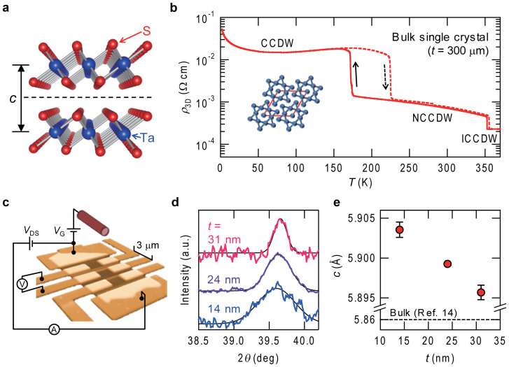
1T-TaS2 (Fig. 1a) is a distinguished correlated metallic TMD, whose rich phase diagram includes an incommensurate (IC), a nearly commensurate (NC), and a commensurate (C) CDW phase (Fig. 1b), as well as a superconductivity phase under pressure17. In the CCDW phase, thirteen Ta atoms form a David-star cluster (Fig. 1b, inset), constructing a triangular superlattice and leading to band reconstruction, whose half-filled band is stabilized by developing Mott state simultaneously18. In the neighboring NCCDW phase, several tens of clusters organize into local CCDW phase domains19. The free electrons in domain boundaries realize the conducting state20.
Figure 1. Basic properties of 1T-TaS2 and its nano-thick crystal device.
(a), The crystal structure of the layered 1T-TaS2, where the sulfur (S) atoms are arranged around the tantalum (Ta) atom on the corners of an octahedron. (b), The temperature dependence of the resistivity (ρ3D) of the bulk 1T-TaS2 single crystal. The solid and broken lines represent the ρ3D in the cooling and warming scan, respectively. The bulk sample showed the ICCDW-NCCDW transition at around 354 K with a hysteresis of 3 K and the NCCDW-CCDW transition at 200 K with a hysteresis of 51 K. Inset: The Ta atom distortions in the CCDW phase, whose reconstructed unit cell is represented by red lines. (c), Schematic of a typical nano-thick crystal device. An ionic liquid is inserted between the floating gate electrode and the crystal to form an EDLT structure. (d), Bragg peaks from (0 0 4) plane of 1T-TaS2 nano-thick crystal devices. The black lines are fits to the Gaussian function. (e), The thickness (t) dependence of the c-axis lattice constant (c). The dashed line represents a typical c value of a 1T-TaS2 single crystal (Ref.14). The error bars represent the numerical ambiguity of the fits.
We prepared many 1T-TaS2 nano-thick crystal devices (see Fig. 1c) whose thickness ranged from 7 nm to 100 nm, and carried out resistivity measurements. Also we performed microbeam X-ray diffraction measurements21,22 in SPring-8 on the nano-thick crystals partially covered with electrodes for resistivity measurements (see Methods).
Results
Microbeam X-ray diffraction measurements
As shown in Fig. 1d, each nano-thick crystal showed a Bragg peak at room temperature and yielded its c-axis parameter slightly larger than that of a bulk single crystal14. A systematic increase in c-axis parameter with decreasing thickness was observed (Fig. 1e), indicating thinning-induced swelling along c-axis. Although such a tendency of swelling with thinning was theoretically proposed for NbSe2 monolayer by the first principle calculation23, it is surprising that such a size effect appears in relatively thick crystals consisting of tens of layers in 1T-TaS2.
Thickness-controlled CDW phase transition
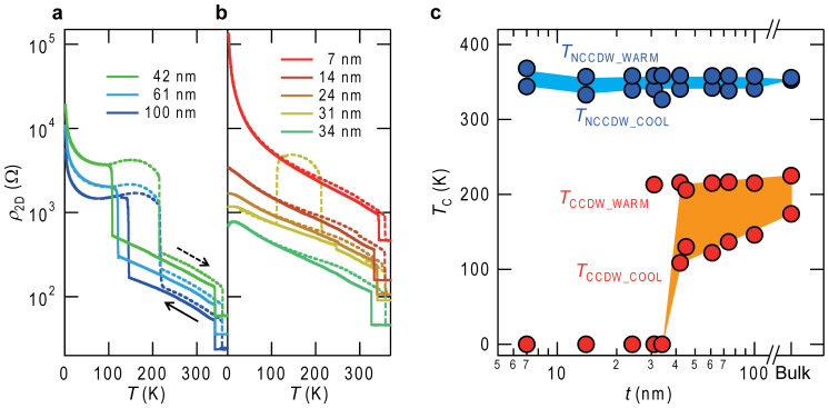
Fig. 2a and 2b show the temperature (T) dependence of sheet resistance (ρ2D, equals to resistivity divided by the thickness) for devices with different thicknesses, recorded at the cooling/warming rate of 1 K/min. The NCCDW-CCDW transition (around 150 K) showed significant thickness dependence while the ICCDW-NCCDW transition (around 350 K) was robust even down to 7 nm. In the crystals thicker than 40 nm (Fig. 2a), the reduction of thickness induced gradual decrease of the NCCDW-CCDW transition temperature (TCCDW_COOL), associated with the hysteresis broadening. By contrast, in crystals thinner than 40 nm (Fig. 2b), the NCCDW-CCDW transition on cooling disappeared and the low resistivity state was kept down to 2 K. In addition, a tiny decrease of resistivity was observed below 20 K in the 34-nm-thick crystal, indicating a formation of metallic state. This metallic behavior was, however, suppressed by further thinning, and the 7-nm-thick crystal showed an insulating state, reminiscent of Anderson localization. This evolution from Mott to Anderson localization through a metallic state resembles the sequence driven by electron-irradiation-induced defects in bulk single crystals24. The thickness dependency of the transition temperatures are summarized in Fig. 2c, unambiguously implying that approximately 40 nm is the critical thickness for the NCCDW-CCDW transition to occur.
Figure 2. Thickness dependent CDW phase transitions of 1T-TaS2 nano-thick crystals.
(a) and (b), The temperature dependence of the sheet resistance (ρ2D) for selected 1T-TaS2 nano-thick crystals. The solid and broken lines represent the ρ2D in the cooling and warming cycle, respectively. (a): Crystals thicker than 40 nm behave similarly to bulk, showing the resistivity anomaly due to the occurrence of both the ICCDW-NCCDW and NCCDW-CCDW transitions. (b): Crystals thinner than 40 nm keep the low resistance state down to low temperatures, consequently realizing the super-cooled state at low temperatures. The 31-nm-thick crystal showed the jump in the warming cycle, indicating a transition from the super-cooled state to CCDW phase. (c), The temperature-thickness (t) phase diagram of 1T-TaS2 nano-thick crystal. The notations TCCDW_COOL (TNCCDW_COOL) and TCCDW_WARM (TNCCDW_WARM) represent the NCCDW-CCDW (ICCDW-NCCDW) transition temperature during the cooling- and warming- cycle, respectively. The shaded area in (c) is intended as a guide for the eyes to capture the width of the hysteresis.
Cooling-rate-controlled CDW phase transition
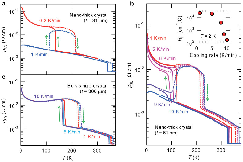
The 31-nm-thick crystal, where the NCCDW-CCDW transition is absent under the cooling rate of 1 K/min, does show an insulating state on warming (Fig. 2b). This transition on warming is not reproducible but certainly occurs in several occasions. This behavior suggests that the NCCDW-CCDW transition is hidden in the measured condition. To gain more insight into the nature of the NCCDW-CCDW transition in thin crystals, we varied the cooling rate. Resistivity (ρ3D) – T curves of the 31-nm-thick crystal under two cooling/warming rates are compared in Fig. 3a. The NCCDW-CCDW transition was clearly recovered when the crystal was cooled with 0.2 K/min. The appearance of the CCDW phase by slow cooling implies the speed of CCDW domains growth in the NCCDW phase is so slow that the high-temperature NCCDW state is quenched.
Figure 3. Cooling-rate dependent CDW phase transitions of 1T-TaS2.
(a), The temperature dependence of the resistivity (ρ3D) for different temperature-sweeping rates in the 31-nm-thick crystal. The solid and broken lines represent the ρ3D in the cooling and warming cycle, respectively. (b), The temperature dependent resistivity of the 61-nm-thick crystal at various sweeping rates, showing the freezing of the NCCDW state by rapid cooling. Inset: The cooling rate dependence of Hall coefficient (RH) at 2 K. The decrease of the RH, i.e. the increase of carriers in domain boundaries indicates the small size of the CCDW domain in the super-cooled state. (c), The temperature dependence of the resistivity for different temperature-sweeping rates in a bulk crystal.
Figure 3b displays an evolution of ρ3D – T curves with the cooling rate for the 61-nm-thick crystal. As the cooling/warming rate was increased from 1 K/min to 8 K/min, the size of the hysteresis became larger, and the resistivity at the CCDW phase was slightly decreased. At 9 K/min, the jump of resistivity appeared at a dramatically low temperature below 100 K, and the resistivity at 2 K became one order smaller than that of 8 K/min. At 10 K/min, the metallic NCCDW state was maintained down to 2 K, in a similar manner to the 31-nm-thick crystal cooled at 1 K/min. This similarity, in conjunction with the fact that the quenching of the NCCDW state does not occur even at 10 K/min for bulk single crystal (Fig. 3c), suggests that the growth speed of CCDW domains is reduced by thinning.
The rapid cooling effect also appeared in the Hall coefficient (RH) (Fig. 3b, inset). RH at 2 K decreased with rapid cooling, and RH of 10 K/min was around two orders of magnitude smaller than that of 1 K/min. The increase of carriers at 2 K indicates that rapid cooling freezes the growth of CCDW domains, leading to shrinkage of CCDW domains and an increase of mobile electrons in the domain boundaries. Nevertheless, it is noted that even under the rapid cooling, the insulating CCDW state was recovered on warming.
Gate-controlled CDW phase transition
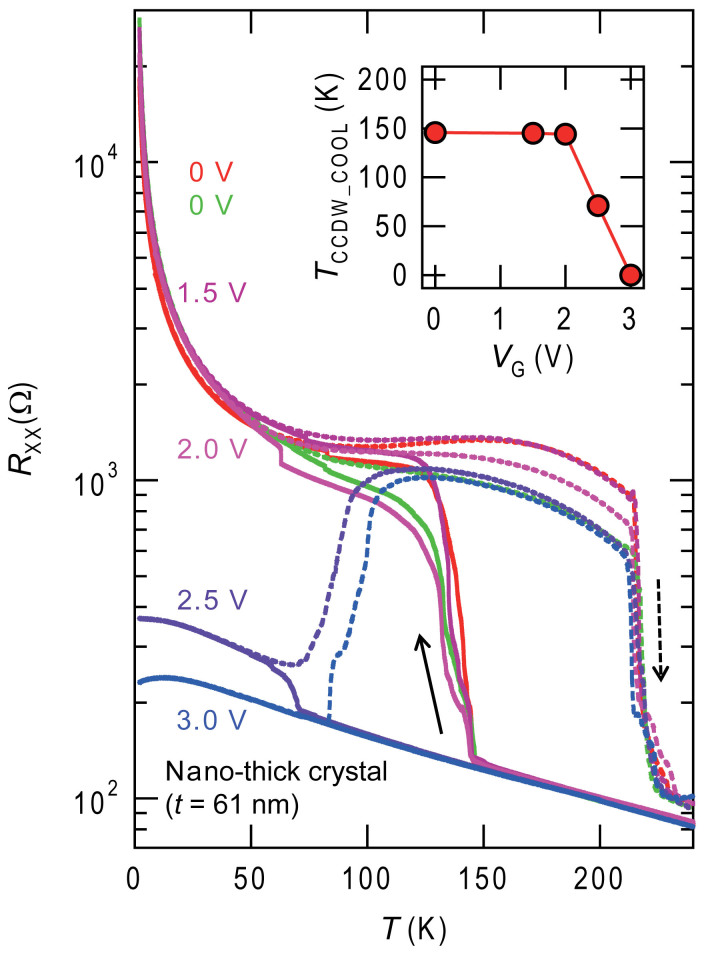
Since the CCDW phase is much more fragile in nano-thick crystals compared to bulk crystals, it can be susceptible to external fields such as electric field, which might enhance the controllability. We made the electric double layer transistor (EDLT) structure with the 61-nm-thick crystal as the channel material, and an ionic liquid (DEME-TFSI) as the gate dielectric25,26,27. We applied gate voltage (VG) at 240 K above the freezing temperature of DEME-TFSI and TCCDW_WARM. As shown in Fig. 4, TCCDW_COOL (145 K) was hardly affected below 2 V. However at 2.5 V, TCCDW_COOL was decreased dramatically down to 71 K. At 3 V, the NCCDW-CCDW transition was completely suppressed on cooling and the metallic state was stabilized below 20 K. The field-induced metallic behavior concurs with that of the super-cooled nano-thick crystal at 10 K/min, indicating whole the crystal was converted into the conducting state by VG. The NCCDW-CCDW transition was completely recovered when VG was reduced to 0 V (green lines in Fig. 4) after gating at VG = 3 V, indicating the gate-induced transition is reversible. The occurrence of the NCCDW-CCDW transition below 2 V excludes the strain effect of frozen ionic liquid on the nano-thick crystal.
Figure 4. Gate-controlled CDW states in a 1T-TaS2 nano-thick crystal.
The temperature dependence of the resistance (Rxx) for a 61-nm-thick crystal with different gate voltages (VG) ranging from 0 V to 3 V. The solid and broken lines represent the Rxx in the cooling and warming cycle, respectively. The red and green curves were taken before and after the gating experiments. Inset shows the TCCDW_COOL-VG phase diagram, where the TCCDW_COOL represents the NCCDW-CCDW transition temperature during the cooling cycle.
The peculiar device operation of 1T-TaS2-EDLT coincides with the characteristic behavior of VO2-EDLT, where VG ( = 1 V) suppressed the first-order metal-insulator transition (MIT)27. It has been claimed that the whole VO2 film up to 70 nm, well above the screening length, was converted to metallic state. The mechanism of gating in VO2 is under debate in terms of gate-induced oxygen deficiency28. In 1T-TaS2, on the other hand, the formation of sulfur vacancy by electric field is not yet known. Combined with the reversible gating operation in TaS2, the electrostatic mechanism is highly likely in the present case, although the final proof is left to be obtained in the future experiment. At least our observation of the gate-induced suppression of MIT in 1T-TaS2 suggests the first-order MIT can be universally controlled by gating.
Discussion
In the present work, we emphasize that the super-cooled NCCDW state was evoked not only by an explicit quenching but also by thinning, which apparently have no relation to the ordering kinetics of a first-order phase transition. The super-cooled state is unique because it seems to be realized only in nano-thick crystals. The origin of the super-cooled state should be directly related to the thinning, i.e. the reduced dimensionality, and the thinning-induced swelling revealed by microbeam X-ray diffraction (Fig. 1e). The CCDW phase is known to have a 3D long-range order with a stacking period of 13 layers, approximately 8 nm29. The expansion of c-axis makes the interlayer overlap of wave functions smaller and reduces dimensionality. Reduced dimensionality may increase the degree of fluctuation and inhibit CCDW domains from growing and interconnecting to each other. Still, the nature of the super-cooled state should be further investigated. High pressure is also known to suppress the CCDW phase but the pressure leads to an increase in wave function overlap17, which is the opposite of the thinning effect. The super-cooled NCCDW state in nano-thick crystals is not necessarily the same as the NCCDW state under pressure in bulk crystals. It can be informative to refer to the “hidden state” recently found by quenching with a single 35-femtosecond laser pulse in 100-nm-thick crystal30, though the two states may be different.
In conclusion, we controlled the NCCDW-CCDW transition and induced the super-cooled NCCDW state in 1T-TaS2 by changing thickness, cooling rate, and gate voltage. The suppression of the NCCDW-CCDW transition and the creation of the super-cooled state are possibly the consequence of the reduced dimensionality caused by the expansion of the c-axis with thinning. More importantly, the CCDW phase in nano-thick crystals is so fragile that electric field can induce the super-cooled state based on the EDLT configuration. The present results demonstrate that nano-thick crystal of 2D material with strong electron correlation has the great potential as a system to disclose the complex nature of correlated electrons and functionalize such novel electronic states.
Methods
Device preparations
The 1T-TaS2 single crystal was grown by the conventional chemical vapor transport method.
Nano-thick crystals were isolated from the bulk single crystal by mechanical exfoliation with Scotch tape, and transferred onto doped silicon wafer covered with a layer of thermally grown silicon dioxide. The typical size of cleaved nano-thick crystals was 10 × 10 μm2. Metal contacts were made by an electron beam lithography process, followed by the sequential deposition of titanium (5 nm) and gold (100 nm). The thickness of the nano-thick crystals was determined by atomic force microscopy (AFM).
The EDLT structure was finalized just before the measurement of gate dependence by putting an organic ionic liquid, N,N-diethyl-N-(2-methoxyethyl)-N-methylammonium bis-trifluoromethylsulfonyl)-imide (DEME-TFSI), which covered both the nano-thick crystal and the gate electrode.
Measurements
Microbeam X-ray diffraction measurements with 12.4 keV were carried out at BL13XU beamline at SPring-8. To determine the c-axis parameter of the nano-thick crystals, we recorded diffraction patterns from the nano-thick crystals on which transport properties were measured, using the microbeam X-ray. The beam size was 0.4 μm in radius, which is small enough to hit the channel area of the nano-thick crystal with electrodes. The position of the channel area was adjusted to a focal point of the microbeam X-ray by monitoring fluorescent X-rays from the gold electrode. The diffraction from (0 0 4) plane was detected and the Bragg peak was fitted by Gaussian function to deduce the c-axis lattice constant.
All the transport measurements were performed in Physical Property Measurement System (PPMS, Quantum Design, Inc.) under He-purged conditions. In the cooling effect measurement, when we cooled down and warmed up with the sweeping rate of 1 K/min or smaller, we maintained the rate in the whole temperature scan. When we measured with the sweeping rate larger than 1 K/min, we cooled down to 50 K with the rapid rate, waited at 50 K until the sample temperature was stabilized to 50 K, cooled down and warmed up between 50 K and 2 K at 1 K/min, and warmed up with the rapid rate.
In the measurement of gating effect, we first cooled down from 300 K to 240 K without gating, applied the gate voltage at 240 K, cooled down and warmed up between 240 K and 2 K, and released the gate voltage at 240 K, followed by warming up to 300 K. All the gating experiment was performed with the scanning rate of 1 K/min.
Author Contributions
M.Y. and Y.J.Z. fabricated the devices, performed the transport measurements, and analyzed the data. J.T.Y. contributed to the device fabrications and the transport experimental setup. R.S. grew the single crystal. Y. Imai, S.K., J.T.Y., Y.J.Z. and M.Y. carried out the microbeam X-ray measurement. M.Y., Y.J.Z., J.T.Y., A.F. and Y. Iwasa planned and supervised the study. M.Y. and Y. Iwasa wrote the manuscript.
Acknowledgments
We are grateful to Y. Kasahara for experimental supports and fruitful discussions. Y. J. Z. is supported by the Japan Society for the Promotion of Science (JSPS) through a research fellowship for young scientists. This work was supported by the Strategic International Collaborative Research Program (SICORP-LEMSUPAR) of the Japan Science and Technology Agency, Grant-in-Aid for Specially Promoted Research (No. 25000003) from JSPS. The synchrotron microbeam X-ray diffraction experiments were performed at the BL13XU of SPring-8 with the approval of the Japan Synchrotron Radiation Research Institute (JASRI) (Proposal No. 2012A1481 and 2013A1355).
References
- Imada M., Fujimori A. & Tokura Y. Metal-insulator transitions. Rev. Mod. Phys. 70, 1039–1263 (1998). [Google Scholar]
- McKenzie R. H. Similarities between organic and cuprate superconductors. Science 278, 820–821 (1997). [Google Scholar]
- Wang Q. Y. et al. Interface-induced high-temperature superconductivity in single unit-cell FeSe films on SrTiO3. Chin. Phys. Lett. 29, 037402 (2012). [Google Scholar]
- Liu D. F. et al. Electronic origin of high-temperature superconductivity in single-layer FeSe superconductor. Nature Commun. 3, 931 (2012). [DOI] [PubMed] [Google Scholar]
- Dagotto E. Complexity in strongly correlated electronic systems. Science 309, 257–262 (2005). [DOI] [PubMed] [Google Scholar]
- Tokura Y. Critical features of colossal magnetoresistive manganites. Rep. Prog. Phys. 69, 797–851 (2006). [Google Scholar]
- Novoselov K. S. et al. Two-dimensional atomic crystals. Proc. Natl. Acad. Sci. U. S. A. 102, 10451–10453 (2005). [DOI] [PMC free article] [PubMed] [Google Scholar]
- Splendiani A. et al. Emerging photoluminescence in monolayer MoS2. Nano Lett. 10, 1271–1275 (2010). [DOI] [PubMed] [Google Scholar]
- Mak K. F. et al. Atomically thin MoS2: a new direct-gap semiconductor. Phys. Rev. Lett. 105, 136805 (2010). [DOI] [PubMed] [Google Scholar]
- Xiao D., Liu G. B., Feng W., Xu X. & Yao W. Coupled spin and valley physics in monolayers of MoS2 and other group-VI dichalcogenide. Phys. Rev. Lett. 108, 196802 (2012). [DOI] [PubMed] [Google Scholar]
- Mak K. F., He K., Shan J. & Heinz T. F. Control of valley polarization in monolayer MoS2 by optical helicity. Nature Nanotech. 7, 494–498 (2012). [DOI] [PubMed] [Google Scholar]
- Zhang Y. et al. Direct observation of the transition from indirect to direct bandgap in atomically thin epitaxial MoSe2. Nature Nanotech. 9, 111–115 (2014). [DOI] [PubMed] [Google Scholar]
- Novoselov K. S. et al. Electric Field Effect in Atomically Thin Carbon Films. Science 306, 666–669 (2004). [DOI] [PubMed] [Google Scholar]
- Wilson J. A. & Yoffe A. D. The transition metal dichalcogenides discussion and interpretation of the observed optical, electrical and structural properties. Adv. Phys. 18, 193–335 (1969). [Google Scholar]
- Wilson J. A., Di Salvo F. J. & Mahajan S. Charge-density waves and superlattices in the metallic layered transition metal dichalcogenides. Adv. Phys. 24, 117–201 (1975). [Google Scholar]
- Morosan E. et al. Superconductivity in CuxTiSe2. Nature Phys. 2, 544–550 (2006). [Google Scholar]
- Sipos B. et al. From Mott state to superconductivity in 1T-TaS2. Nature Mat. 7, 960–965 (2008). [DOI] [PubMed] [Google Scholar]
- Fazekas P. & Tosatti E. Charge carrier localization in pure and doped 1T-TaS2. Physica 99B, 183–187 (1980). [Google Scholar]
- Spijkerman A., de Boer J. L., Meestsma A., Wiegers G. A. & Smaalen S. X-ray crystal-structure refinement of the nearly commensurate phase of 1T-TaS2 in (3+2)-dimensional superspace. Phys. Rev. B 56, 13757–13767 (1997). [Google Scholar]
- Zwick F. et al. Spectral Consequences of Broken Phase Coherence in 1T-TaS2. Phys. Rev. Lett. 81, 1058–1061 (1998). [Google Scholar]
- Takeda S., Kimura S., Sakata O. & Sakai A. Developemt of high-angular-resolution microdiffraction system for reciprocal space map measurements. Jpn. J. Appl. Phys. 45, L1054–L1056 (2006). [Google Scholar]
- Imai Y., Kimura S., Sakata O. & Sakai A. High-angular-resolution microbeam X-ray diffraction with CCD detector. AIP Conf. Proc. 1221, 30–33 (2010). [Google Scholar]
- Calandra M., Mazin I. I. & Mauri F. Effect of dimensionality on the charge-density wave in few-layer 2H-NbSe2. Phys. Rev. B 80, 241108(R) (2009). [Google Scholar]
- Mutka H., Zuppiroli L., Molinie P. & Bourgoin J. C. Charge-density waves and localization in electron-irradiated 1T-TaS2. Phys. Rev. B 23, 5030–5037 (1981). [Google Scholar]
- Shimotani H. et al. Insulator-to-metal transition in ZnO by electric double layer gating. Appl. Phys. Lett. 91, 082106 (2007). [Google Scholar]
- Ye J. T. et al. Superconducting dome in a gate-tuned band insulator. Science 338, 1193–1196 (2012). [DOI] [PubMed] [Google Scholar]
- Nakano M. et al. Collective bulk carrier delocalization driven by electrostatic surface charge accumulation. Nature 487, 459–462 (2012). [DOI] [PubMed] [Google Scholar]
- Jeong J. et al. Suppression of metal-insulator transition in VO2 by electric field-induced oxygen vacancy formation. Science 339, 1402–1405 (2013). [DOI] [PubMed] [Google Scholar]
- Moncton D. E., Di Salvo F. J., Axe J. D., Sham L. J. & Patton B. R. Charge-density wave stacking order in 1T-Ta1-xZrxSe2: Interlayer interactions and impurity (Zr) effects. Phys. Rev. B 14, 3432–3437 (1976). [Google Scholar]
- Stojchevska L. et al. Ultrafast switching to a stable hidden quantum state in an electronic crystal. Science 344, 177–180 (2014). [DOI] [PubMed] [Google Scholar]


