Abstract
Rectangular pulses applied to disk electrodes result in high current density at the edges of the disk, which can lead to electrode corrosion and tissue damage. We explored a method for reducing current density and corrosion, by varying the leading edge of the current pulse. Finite element modeling and mathematical analysis were used to predict an optimal waveform that reduces current density at the edge while also maintaining short pulse duration. An approximation of the optimized waveform was implemented experimentally and applied to platinum disk electrodes. Surface analysis using energy-dispersive spectroscopy (EDS) showed significant reduction of corrosion on the periphery of these electrodes after pulsing, compared to those pulsed with the control rectangular waveform.
Index Terms: Current density, edge effect, double layer, neural stimulation, biomedical electrodes
I. INTRODUCTION
Disk electrodes are commonly used in biomedical and electrochemical applications. Current density and potential distributions on the electrode-electrolyte interface have been carefully examined [1]–[4]. Newman’s analytical solution concludes that the electric field and thus current density are both sharply enhanced at the periphery of the electrode [1]. He shows that the primary current density exhibits a singularity at the very edge, whereas being only half the average value at the center of the disk. While methods like charge balanced biphasic stimulation etc. have become the norm to reduce charge accumulation, it doesn’t prevent the locally enhanced current density to drive electrochemical reactions at the disk edge and thus corrode the periphery of the electrode. Tissue damage due to localized stimulation is of concern in biomedical applications [5], [6].
Several different approaches to reduce this undesired behavior have been proposed, mainly by altering the geometric design of the electrode [4], [6]–[10]. The segmented circular electrode consists of a set of annular rings around a central circular electrode. By placing resistors in series with the conducting line to each segment, current can be distributed more evenly [4]. Gradient of resistivity on surface achieves the same goal [6], [11]. Designs of electrode recessed into the substrate have been discussed by several groups, with the focus on reducing the non-uniformity of current density on the surface of the electrode but not necessarily at the aperture of the recess [7]–[10], [12]. Application of a resistive layer over the electrode surface has shown a more uniform current density distribution in certain applications [10], [13]–[14]; however this might increase the overall impedance to an unacceptable level.
In these methods, the main focus is altering the primary current distribution, while the secondary distribution due to the double layer capacitance and Faradaic reactions are not taken into considerations. These two components of the electrode-electrolyte interface cause the primary current distribution to redistribute to a more uniform secondary profile [3], [15], [16], but these components have only recently been considered in modeling studies [17]–[19]. Behrend et al. have proposed an approach to achieve more uniform current density profiles by re-shaping, i.e. slowing, the rising edge of the input current pulse [18], while a similar idea was explored for voltage pulses [19]. In an earlier study, we have quantitatively examined this approach utilizing finite element model (FEM) technique and shown that a simple ramp (in place of a step) can reduce the edge effect [20].
In this study, an optimized current distribution method was achieved. A FEM study compared the effect of different waveforms and transition lengths. Mathematical analysis further demonstrated the spatial and temporal factors contributing to the non-uniformity of current distribution, leading to an optimal current waveform via numerical solution. Finally, an approximation of the optimized waveform was implemented and applied to platinum disk electrodes, which showed a significant reduction of corrosion on the periphery (versus electrodes pulsed with rectangular pulses).
II. METHODS
A. Finite Element Modeling
1) Model
A finite element model was used, similar to the one proposed by Behrend et al. [18] with slight improvements [20] See [18] (Fig. 1–Fig. 3), [20] (Fig. 1) for details and validation of FEM modeling method. In short, an axial-symmetric system was built in COMSOL Multiphysics v4.2a (COMSOL, Burlington, MA), with a disk electrode of radius α embedded in and coplanar with a flat insulating substrate. The electrode-electrolyte interface consisted of distributed impedance with a capacitive component (γ) as the double layer capacitance per unit area. The electrolyte above the electrode was limited to a semi-spherical space with a radius of 20α, and the rest of the semi-infinite space was approximated and replaced with a series resistance leading to the distant ground. The input current waveforms applied to the disk electrode were given by functions specified within the model. For data analysis, results were exported to MATLAB (The MathWorks, Natick, MA). All space and time variables were normalized to the disk’s radius α, and the electrode’s characteristic time constant τ. The time constant is defined by the electrolyte resistance Rs and the double layer capacitance Cd1
| (1) |
where the theoretical resistance of the semi-infinite medium of conductivity κ above the electrode is given by [1]
| (2) |
and the double layer capacitor is
| (3) |
Fig. 1.
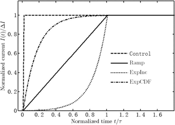
Three different current waveforms are shown with control. Test waveforms are given for one transition length as an example. Time constants of the ExpInc and ExpCDF waveforms are one sixth of the corresponding transition length.
Fig. 3.
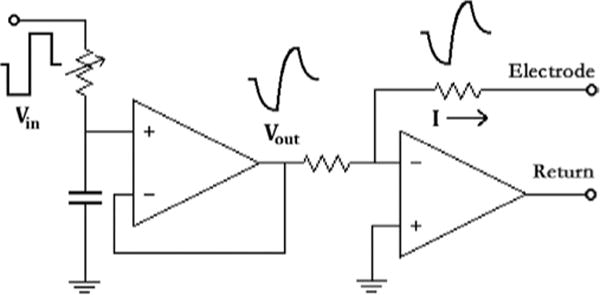
A diagram of the circuit to convert square voltage pulses to the desired current waveform.
2) Current Waveforms
Input waveforms include the standard step input as control and waveforms with different rising edges, respectively. Three different waveforms were tested in combination with three different transition times T, which were set to τ/2, τ or 2τ. The test waveforms include linear ramp (Ramp), exponential increase (ExpInc), and the cumulative distribution function of exponential distribution (ExpCDF), which are described by (4). All current pulses reached the same steady state amplitude I0
Fig. 1 shows the three different waveforms with transition time equal to τ for instance.
| (4) |
The Ramp was tested in the previous study [20], and is included for comparison. It has abrupt transitions at both beginning and end of the ramp. In contrast, the ExpInc and ExpCDF waveforms were chosen to test the effect of having smooth versus abrupt transitions at the beginning or end of ramping phase. Their time constants τX were both set to 1/6 of the corresponding transition length. This choice of the time constant makes the ExpInc waveform start at less than 0.25% of I0, and the ExpCDF waveform reach 99.75% of I0, to smooth the beginning and end of transition, respectively. The waveforms themselves would assure abrupt transition on the other side. In the modeling and mathematical analysis, waveform shaping was studied on only the leading edge of the step input, and results for both monophasic and biphasic rectangular waveforms used in neural stimulation can be easily obtained utilizing the linearity of the system.
3) Data Analysis
All modeling output data were normalized. The theoretical initial voltage corresponding to the step input (5) is used for potential normalization, and the average geometric current density at steady state (6) is used for current density normalization.
| (5) |
| (6) |
Two quantities were calculated to compare the current density overshoot above the average current density at steady state [20]. The maximal current density at any given time was analyzed using
| (7) |
A small annular region on the edge was excluded due to the singularity and the analysis was performed over the region of r ≤ 0.9995α.
Besides the maxima, the area-weighted average of surplus current density compared to steady state average value was calculated and normalized to present the current amplitude that exceeded the desired uniform steady state distribution. This dimensionless value is defined as Current Overload (CO)
| (8) |
Current Overload Index COI is the accumulated CO
| (9) |
which gives an indication of how much damage would be caused by the edge enhancement if average current density was to be set to the safety limits of the electrode. A more comprehensive analysis could also include corrosion or other damage as a function of the current overload into the weight for the calculation of CO, which is not discussed here.
B. Mathematical Analysis
1) Current Step Response of Disk Electrodes
Nisancioglu and Newman analyzed the step response of a disk electrode subject to current input utilizing the transition from cylindrical coordinates to rotational elliptic coordinates and gave analytical solutions [3]. Both double layer capacitance and Faradaic reactions were included.
Our further analysis assumes no Faradaic reactions however, due to its minimal effect on the spatial and temporal distribution of current density (results not shown). Typical micro-electrodes in neural engineering application work with pulses in the micro- to millisecond range, with Faradaic reactions having much smaller conductance compared to the electrolyte conductance. In the one time constant model of electrodes, the parallel resistance of the reactions is in the megaohm to gigaohm range (i.e. a low conductance), compared to kiloohm values of the series resistance of the electrolyte (i.e. higher conductance). Also, most electrodes used in neural implants are highly capacitive (or pseudocapacitive) as Faradaic reactions are not desired due to their irreversibility and potential harm to tissue.
Solving for the Step Response (SR) involves decomposing it into Steady-State (SS) and Transient (TZ) components [3], here with the current density given as example:
| (10) |
The first term represents the stable response to a constant current of amplitude I0, i.e. secondary distribution. The transient response doesn’t contribute to the overall current input to the electrode. However, it is responsible for the actual distribution of current density on the electrode surface and its shift from the initial condition immediately after the input onset (t = 0+) to steady state distribution, i.e. primary to secondary. As the boundary condition of the electrode-electrolyte interface is described with a first order differential equation with respect to time, the transient component is further decomposed into eigensolutions. These two components will be further discussed in Results.
2) Constructing Arbitrary Response from the Step Response
For any input x(t), the output y(t) could be given as the convolution of the input and the impulse response h(t) as
| (11) |
or alternatively by the step response g(t) = ∫ h(t)dt as
| (12) |
The desired current waveform will reduce the current density non-uniformity; therefore the input I(t) = I0 · x(t) should satisfy the following condition:
| (13) |
The second criterion states that x(t) is continuous and increases monotonically. The last criterion indicates a reasonably short transition time period for the input current to converge to its final amplitude, so that the modification to the rectangular pulses commonly used in neural stimulation would not distort the overall pulse shape too much. Otherwise it may alter the neural response to stimulation. In these applications the initial value of the input is conveniently set to zero, further simplifying (12) to
| (14) |
Applying (14) to the results of (10) above, the current density response to the arbitrary input I(t) could be given as
| (15) |
which provides the mathematical foundation of the waveform shaping method. The first term shows that the time domain contribution of the steady-state component in the output is just scaled by the input waveform, and quickly converges to the same secondary distribution as the step response. The contribution of the transient component, which the non-uniformity of the overall current density profile is due to, is in the second term. Hence the high peripheral current density could be reduced if the input’s time derivative ẋ(t) is small in amplitude, i.e. smooth transition. The transient component diminishes as condition (13) indicates that
| (16) |
3) Numeric Optimization
Due to the complexity of the analytical solution, a numeric solution has been developed to estimate the optimum waveform to reduce the local current density overshoot above the steady state situation.
The numeric method is based on a discrete-time version of (12). The output is built by stacking scaled unit step responses carefully so that the total response does not exceed a certain level (e. g. ). The input is therefore determined by coefficients used to the scale the unit step response. To implement this, the normalized step response (simulated or analytical solution) is sampled with time intervals ∆t = 0.01τ over a long enough time (e.g. t ≥ 3τ).
| (17) |
The calculation was again limited to r ≤ 0.9995α. An Overshoot Limit OSL is introduced to allow some tradeoff between overshoot above the steady state current density during the transition and the length of the transition time. The overshoot limit is a number equal or larger to 1, and restricts the current density within the analyzed region to
| (18) |
The flowchart for the algorithm is shown as follows in Fig. 2, and an example is given to show the concept of composing the input and output in Fig. 3. Optimal current waveforms, as well as the best-fit ExpCDF waveforms were calculated for different OSLs.
Fig. 2.
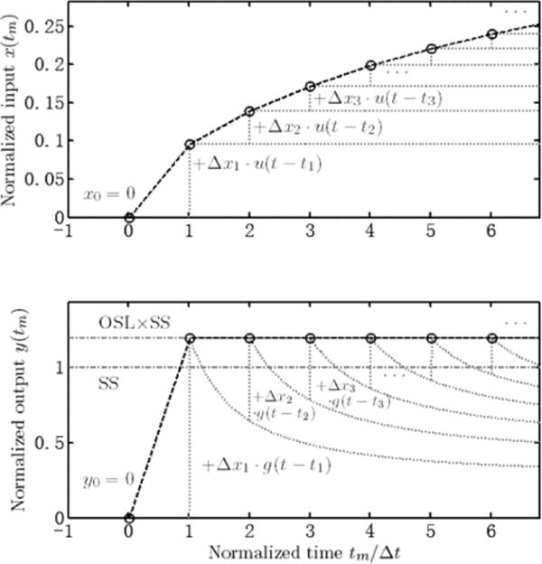
1-dimensional example plot explaining the algorithm in Fig. 2. The black dashed line represents the optimized input and output with the sampling points (circles). The grey dotted lines are the underlying step inputs and step responses that the sampled input and output are built of. At each time step, the size of the additional step of input is first determined by the output, and then a scaled step and step response are added to the total input and output. The lines SS and SS × OSL in the bottom figure indicated the normalized steady state response and the allowed overshoot, which is set to 20% here for example (OSL = 1.2).
C. Pulsing Experiments and Surface Analysis
1) Circuit Setup
The best-fit ExpCDF of the optimum current waveform is implemented by converting a square voltage pulse from a Model 2100 Isolated Pulse Stimulator (A-M Systems, Sequim, WA) into the desired waveform with a RC circuit, which was then converted into a current pulse of the same shape by operational amplifier and delivered to the electrode. A simplified circuit diagram is shown in Fig. 4. The RC circuit has a variable resistor adjusting its time constant, hence the transition time of the waveform. A buffer stage was added in between for stability and impedance matching. For the control group, the RC circuit was omitted, and the voltage pulses were directly applied to the buffer stage.
Fig. 4.
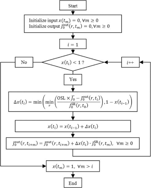
Flow chart for deriving the numerical optimal waveform.
2) Electrodes
An Epilepsy/Long-Term Monitoring Subdural Electrode Array (Ad-Tech Medical Instrument Corporation, Racine, WI) was used for its consistent fabrication quality and large electrode size. The 8×8 array contained platinum electrodes of 4 mm diameter, with the center of 2.3 mm diameter being exposed. Electrochemical Impedance Spectroscopy (EIS) using Gamry Reference600™ (Gamry Instruments, Warminster, PA) showed that the average access resistance of the electrode is 220 Ω in phosphate-buffered saline (PBS), and the average double layer capacitance is 3.4 μF. The characteristic time constant is therefore approximately 0.75 ms. The parallel resistance is on the order of 100 MΩ.
3) Pulsing Protocol
The electrodes were pulsed in PBS with a thick platinum wire as return electrode. The pulsing protocol consisted of cathodic-first biphasic pulses at a frequency of 50 Hz for 20 minutes [21]. The pulse width of each phase was 2 ms in duration. The control group was pulsed with rectangular pulses. The test group was pulsed with ExpCDF current pulse with a time constant of 0.4 ms, about half of the electrode’s time constant. In both groups, the current amplitude was set so that the potential excursion of the electrode-electrolyte interface reached to ± 1.5 V at the end of each phase. As a result, potential on the electrodes’ surface would exceed the water window (−0.6 V to 0.9 V) to cause corrosion [21]. For the test waveform, the potential excursion across the electrode-electrolyte interface was verified by subtracting the potential caused by ohmic drop due to electrolyte resistance from the total measured potential. The corresponding current levels for both situations were on average 5 mA, equivalent to 240 μC/cm2 per phase. The sizes of the test and control groups were 5 and 4 electrodes respectively, while 2 more unused electrodes were used for baseline in the surface analysis.
4) Surface Analysis
After current pulsing, the electrodes were detached from the substrate and cleaned with deionized (DI) water. Scanning electron microscope (SEM) was used to investigate the surface morphologies of the electrodes (JEOL JSM-6610, JEOL USA, Inc., Peabody, MA). Chemical compositional analyses of the pulsed electrodes were performed using EDS. For each electrode, three evenly distributed diameters across the exposed surface were randomly chosen and scanned. For each diameter, EDS data were collected from 20 evenly spaced spots with 15 kV acceleration voltage and 25 second collection time at each spot. The data is equivalently from 6 radii, with 10 data points per radius. Atomic count percentage of platinum and oxygen on the electrode surface were analyzed by EDAX Genesis program (EDAX Inc., Mahwah, NJ), and transferred to MATLAB for further analysis.
III. RESULTS
A. Comparison of Different Current Waveforms
The normalized maximal current density (within r ≤ 0.9995a) is plotted versus time in Fig. 5. The peak maxima are compared to the average steady state current density , and expressed as an excess percentage
| (19) |
Fig. 5.
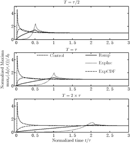
Normalized current density maxima within r ≤ 0.9995α versus time for three different transition lengths and different waveforms. All converge to unity as secondary distribution prevails through different time course.
The control input resulted in peak overshoot of almost 4 times steady state (364.9%) before decaying to the average value. All the different test current waveforms have much smaller peak maximal current densities, with detailed values for each waveform and transition length combination given in Table I. The ExpInc has the least improvement of all three candidate waveforms at each transition lengths, with peak overshoot at least half the steady state; the Ramp and ExpCDF are markedly better than ExpInc. The Ramp is best for short transition length and has slightly less improvement compared to ExpCDF for intermediate and long transition lengths. The ExpCDF has an extremely low peak overshoot for 2τ transition length.
The CO as function of time is given in Fig. 6. The COI for the current step is equal to 0.0585, and the reduction for each combinations is given in Table II. A similar trend is seen for COI compared to the peak overshoot. However, the difference between ExpInc and the other two waveforms are not as large, and the Ramp has better performance compared to ExpCDF for intermediate transition length. Again, ExpCDF performed extremely well for 2τ transition length.
Fig. 6.
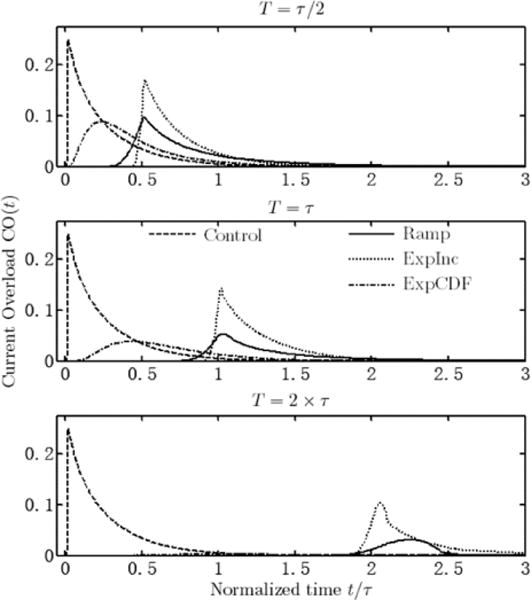
Current Overload (CO) versus time for three different transition lengths and different waveforms. All decay to zero as secondary distribution prevails, however accumulation differs. The CO of ExpCDF waveform with 2τ transition length is very small and barely visible in the bottom graph.
TABLE II.
NORMALIZED COI FOR DIFFERENT WAVEFORMS AND TRANSITION
|
|
Ramp | ExpInc | ExpCDF | |
|---|---|---|---|---|
| T = τ/2 | 67.43% | 81.35% | 75.72% | |
| T = τ | 39.49% | 72.34% | 45.27% | |
| T = 2τ | 21.92% | 55.16% | 5.50% |
B. Mathematical Analysis
1) Transient Solution
The transient response of the step input is given by a further decomposition into exponential decaying eigensolutions with spatial profiles and time constants τ(i) [3]
| (20) |
Each eigensolution corresponds to an eigenvalue λ(i), which is related to the time constant by
| (21) |
where Λ(i) is the normalized eigenvalue
| (22) |
Due to the normalization with τ, the normalized eigenvalues are scaled by π/4 compared to the original values given by Nisancioglu and Newman [3]. Normalized eigenvalues are calculated in increasing order (according to increasing value), along with their corresponding eigensolutions. The first ten normalized eigenvalues are given in Table III, and their eigensolutions are given in Fig. 7 (generated according to [3]).
TABLE III.
FIRST TEN NORMALIZED EIGENVALUES.
| i | 1 | 2 | 3 | 4 | 5 |
| Λ(i) | 3.237 | 5.766 | 8.260 | 10.74 | 13.22 |
|
| |||||
| i | 6 | 7 | 8 | 9 | 10 |
| Λ(i) | 15.69 | 18.17 | 20.64 | 23.11 | 25.58 |
Fig. 7.
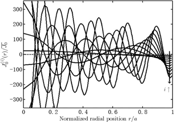
Normalized current density versus radius for the first ten normalized eigensolutions.
It can be observed that the current density at the edge is not the highest for each eigensolution. The current densities towards the center of the disk have larger amplitude but alter in sign and virtually cancel out each other when they are scaled by the coefficients C(i) and summed to form the transient solution. At the edge however, the current density monotonically increases in amplitude with the order of the eigensolution. This leads to the high peripheral current density of the primary distribution. Therefore the desired input current waveform should reduce the contribution of higher order eigensolutions to the transient response as much as possible.
Equation (21) indicates that the time constant of eigensolutions decreases with increasing order. Therefore higher order eigensolutions’ time course have broader spectrum and contain more high frequency components. To suppress the higher order eigensolutions, the derivative of the input ẋ(t) should be a low pass filter. One simple implementation is to use an ExpCDF as explored in the modeling section, whose derivative is
| (23) |
with .
Smaller X reduces the amplitude of ẋ(t), and hence the overall transient component in the response as discussed in (15). Furthermore, it can be demonstrated that for any i, the smaller X is compared to λ(i), the less this eigensolution contributes to the overall response (derivation not shown). Therefore for effective reduction of higher order eigensolutions, the exponential decay of the input should have
| (24) |
with i0 being a small integer, e.g. i0 = 1 or 2. Therefore the corresponding time constant
| (25) |
In the modeling section, ExpCDF waveforms have times constants of 1/6 of the transition time lengths. Hence for the three transition time lengths used, the i0’s are 5, 3, and 1 respectively:
| (26) |
The results showed that the ExpCDF waveforms with transition time length of 2τ indeed reduced the current density maxima and current overload index to an extremely low level. This is further verified in the computational optimization section.
2) Computational Optimization
Based on the algorithm, the optimal waveforms for a few OSL values are given as solid lines in Fig. 8, with the dashed lines being their best-fit ExpCDF waveforms. The corresponding X’s and the COI of optimal and best-fit waveforms are shown in Table IV.
Fig. 8.
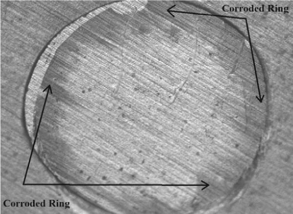
Typical corrosion profile after pulsing.
TABLE IV.
PARAMETERS AND COI OF OPTIMIZED WAVEFORMS AND THEIR FITTED EXPCDF WAVEFORMS FOR SEVERAL OSL.
| OSL | 1.0 | 1.1 | 1.2 | 1.4 | 1.7 | 2.0 |
|---|---|---|---|---|---|---|
| COIopt/COIctrl | 0.0% | 17.8% | 32.3% | 52.0% | 68.2% | 77.1% |
| X · τ | 2.61 | 3.43 | 4.21 | 5.80 | 8.24 | 10.80 |
| τX/τ | 0.383 | 0.292 | 0.237 | 0.173 | 0.121 | 0.093 |
| COIX/COIctrl | 1.38% | 10.10% | 21.47% | 40.51% | 58.59% | 69.28% |
Comparing X with the eigenvalues, there will be almost no overshoot within r ≤ 0.9995α, for X < λ(1). For X < λ(2), the overshoot is less than 40.5% (OSL = 1.4) of the average steady state current density. The fact that the optimum waveforms obtained by the algorithm resemble ExpCDF waveforms allows a relative simple circuit to generate such stimulation waveforms (see methods).
3) Experimental Implementation
Current pulses were applied to platinum electrodes to validate the model, as described in methods. Rectangular pulses were applied to 4 electrodes and ExpCDF pulses applied to 5 electrodes. After pulsing, the surface of the disk electrodes showed yellowish coloration on the periphery in both groups, indicating corrosion due to oxidation of platinum (Fig. 9, arrows). This coloration was evident in both rectangular and ExpCDF pulses.
Fig. 9.
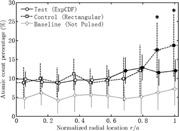
Atomic count percentage of oxygen along disk radius. The data points were slightly offset at each location for clarity. Error bars show standard deviation. Asterisks indicate significant difference between test and control groups. Filled and empty markers indicated center and periphery subgroups within each group. The grey marker of test group is transition between center and periphery subgroups.
EDS was performed on the surface, giving the atomic count percentage of the two major identified elements, platinum and oxygen. Fig. 10 shows the atomic count percentage values averaged across the radii within each group of electrodes versus the radial location with the error bars showing standard deviation. At each location, the mean oxidation levels for the test group (black solid line), the control group (black dashed line), and the baseline (gray solid line) were compared using one-way analysis of variance (ANOVA, α = 0.05). The null-hypothesis that the three groups have equal mean oxidation levels was rejected at all locations (p ≤ 0.002). Further multiple comparison tests were performed using the Tukey’s Honestly Significant Difference (HSD) criterion to compare group means and determine the source of the significant difference(s). The oxidation levels of the test group were significantly lower on the periphery (asterisks) compared to the control group, suggesting that the periphery current density was indeed reduced with the test waveform. As expected, the oxidation level for the baseline group was significantly lower, compared to either test group or control group at any location.
Fig. 10.
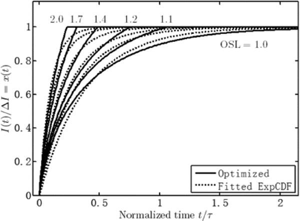
Optimized current waveform obtained from mathematical analysis for reduction of current density on the periphery of disk electrodes, and the best-fit ExpCDF waveforms. Both axes are normalized.
ANOVA within groups shows change of oxidation level across the radius for the test and control groups. Based on the significant difference from ANOVA analysis, the radial locations were divided into two subgroups, the center and periphery. For the control group, the two outer points (asterisks) and the 8 center points showed significant difference in oxidation level, which almost doubled from about 9.89% on average at the center to 18.07% on average on the edge. For the electrodes tested with the modified pulse, the 4 outer points differ from the 5 center points significantly, with one transition point in between. The transition point was statistically different from only to 2 of the 4 peripheral points. The oxidation level stayed relatively uniform around 9.46% in the center, only slightly increasing by one third to 12.12% on the edge. Hence the increase of oxidation level for the control group is much stronger within a narrower region compared to the test group. The baseline has a relatively uniform oxidation level on average of 5.53% with no significant fluctuation. The above results indicate that the pulsing induced oxidation in both control and test pulse groups, however greater oxidation was noted at the edge of the control pulse electrode.
IV. DISCUSSION
This work provides comprehensive examination of the current waveform shaping method to reduce periphery current density on disk electrodes. Analytical and numerical calculations yielded a prediction for an optimal waveform and transition length. Pulsing experiment verified the effectiveness of the method on platinum electrodes.
A. Comparison on Different Approaches
Finite element modeling and analytical studies provided insight and quantitative description to explain the mechanisms behind the current waveform shaping method. The double layer capacitance is responsible for the current density redistribution from the highly non-uniform primary distribution to the more uniform secondary distribution. The waveform shaping exploits this and increases its effect, allowing the current density to redistribute over longer time. From the mathematical standpoint, current waveform shaping suppresses contribution of the higher order eigensolutions to the transient response, which the edge effect mostly relies on.
The modeling and analysis assume ideal conditions, and therefore have certain limitations [13]. The electrodes were assumed to have perfectly smooth surfaces and an ideal seal at electrode-insulator interface. A rough surface would increase the current density at locations of small curvature, therefore increasing the overall current non-uniformity. This is however a small factor compared to the ideally infinite edge effect unless the insulation of the electrode was very defective due to manufacturing failure. A non-perfect electrode-insulator interface would cause leakage of current originating from the electrode-electrolyte interface under the insulation. Non-ideal electrical properties at the edge decrease the edge effect. However, an edge effect would exist and the current shaping method would still help reduce the non-uniformity.
The electrode-electrolyte interface has been as well. The double layer capacitance was assumed to be an ideal capacitor, although it is often better described as a constant phase element (CPE), whose parameter might vary depending on many factors like frequency and bias potential [2], [22]. The Faradaic components were excluded from the analysis and the FEM modeling. This leads to further deviation from reality, especially for large overpotentials, such as those used in the pulsing experiment.
The electrode was symmetric in geometry and referenced to an infinite ground, and the conducting media was isotropic. In reality, the electrolyte space is finite and of arbitrary geometry. In neural stimulation applications, the complex environment of surrounding tissue may change the electrical field and current distribution. Nevertheless, the experimental results demonstrated the effectiveness of the current shaping method despite the above mentioned simplifications and other factors such as the slight recession of the electrodes used.
B. Trade-Off Considerations
Utilization of the proposed method must consider several trade-offs. To achieve the reduction in current density at the periphery will require a rising leading edge, not a step. To minimize edge effects throughout the entire pulse, a transition zone should be added wherever a discontinuity exists in the waveform, which for a rectangular pulse is at the beginning and end of the pulse as edge effect is noted at pulse offset as well. The total charge injection would remain the same for the modified pulse, only increasing the overall pulse width. This has the effect of making the pulse longer. A longer pulse is generally less efficient at stimulating nerves, so more charge may required for the modified pulse to have the same effect as the square pulse. While the peak current density may be minimized, the stimulation may be less efficient.
A secondary consideration when increasing pulse width is the limitation this may place on pulse rate (the number of pulse/second). For example, a pulse width of 2 ms (1 ms/phase) can be repeated at up to 500 pps. Lengthening the pulse would reduce the rate at which pulses can be applied. However, rarely are pulses applied so rapidly, thus this issue is unlikely to be a significant limitation. For example, a micro-rough platinum electrode array with 200 μm diameter has a time constant of 0.43 ms tested in vitreous or 0.98 ms when placed on the retina in vitro [23]. The same type of electrodes in the Argus II Retinal Prosthesis use pulse widths of 0.5 ms at rates of 20 pulses per second. The pulse intervals are therefore 50 ms on average, and there is enough room to accommodate a modification to the pulses.
C. Stimulation Safety and Efficacy
Reducing the edge effect may improve device safety since neural damage is related to current and charge density. The biological safety limit of neural stimulation is variable, and depends on both charge per phase and charge density [23]. An analysis of experimental data has shown that stimulation is not damaging to neurons with higher charge density when using smaller charge per phase. On the other hand the electrochemical safety limit is a constant charge density. Therefore given a small charge per phase, smaller electrode could reach electrochemical safety limit before biological safety limit, necessitating protection through methods like waveform shaping. Larger electrodes may be restricted by biological safety (vs. electrochemical safety) limits, so waveform shaping may be less important in these application.
The high current density is transient in time and limited to near the surface of the electrode. Current nonuniformity decays rapidly away from the electrode surface, even in the primary distribution. Therefore it is reasonable to expect that waveform shaping will have little effect on the neural response, especially in the situations where the electrodes could not be placed close enough to the stimulation target. Retinal prostheses use circular electrodes with rectangular pulses, but the subjects do not describe annular perceptions [25]. Calcium fluorescence imaging studies of in vitro retina do not show preferential neural activation at the edges of 0.2 mm diameter electrodes [26], [27]. In contrast, annular skin burns have been noted after defibrillation, but these electrodes are large (several centimeters) and the skin is adjacent to the surface of the electrode [10], [28]. With microelectrodes (less than 1 mm in diameter), the edge effect is limited in time and space.
V. CONCLUSIONS
The objectives of this study were to investigate the method of shaping current waveform to reduce periphery current density on disk electrodes. Three approaches were used: finite element modeling, mathematical analysis and numeric optimization, and pulsing experiment. The first two gave consistent conclusion on the optimal waveform and transition length, and experiment verified the effectiveness of the method on platinum electrodes.
Further development of this method includes exploring its efficiency on electrodes of different shapes and sizes (for example, cylindrical electrodes as used in deep brain stimulation or cardiac pacing), engineering simple and feasible implementation of the current source, and studying the possible benefits in potential biomedical applications.
TABEL I.
MAXIMUM OVERSHOOT PERCENTAGE OF CURRENT DENSITY MAXIMA
| P max | Ramp | ExpInc | ExpCDF |
|---|---|---|---|
| T = τ/2 | 48.39% | 143.95% | 62.18% |
| T = τ | 25.23% | 102.18% | 23.97% |
| T = 2τ | 9.50% | 50.05% | 2.49% |
Acknowledgments
SEM and EDS data used in this article were generated at The Center for Electron Microscopy and Microanalysis (CEMMA) of the University of Southern California (USC).
This work was supported by Biomimetic MicroElectronic Systems Engineering Research Center (BMES ERC) of the National Science Foundation (NSF), Grant No. EEC-0310723 and the National Institutes of Health, Grant No. U01 GM104604. Asterisk indicates corresponding author.
Contributor Information
Boshuo Wang, Email: boshuowa@usc.edu, Department of Biomedical Engineering, University of Southern California, Los Angeles, CA 90089 USA.
Artin Petrossians, Email: apetross@usc.edu, Mork Family Department of Chemical Engineering and Materials Science, and Department of Ophthalmology, University of Southern California, Los Angeles, CA 90089 USA.
James D. Weiland, Email: jweiland@usc.edu, Department of Ophthalmology and Department of Biomedical Engineering, University of Southern California, Los Angeles, CA 90089 USA.
References
- 1.Newman J. Resistance for flow of current to a disk. J Electrochem Soc. 1966 May;113(5):501–502. [Google Scholar]
- 2.Newman J. Frequency dispersion in capacity measurements at a disk electrode. J Electrochem Soc. 1970 Feb;117(2):198–203. [Google Scholar]
- 3.Nisancioglu K, Newman J. The transient response of a disk electrode. J Electrochem Soc. 1973 Oct;120(10):1339–1346. [Google Scholar]
- 4.Wiley JD, Webster JG. Analysis and control of the current distribution under circular dispersive electrodes. IEEE Trans Biomed Eng. 1982 May;BME-29(5):381–385. doi: 10.1109/TBME.1982.324910. [DOI] [PubMed] [Google Scholar]
- 5.Overmyer KM, Pearce ja, DeWitt DP. Measurements of temperature distributions at electro-surgical dispersive electrode sites. Trans ASME, J Biomech Eng. 1979 Feb;101(1):66–72. [Google Scholar]
- 6.Kim Y, Fahy JB, Tupper BJ. Optimal electrode designs for electrosurgery, defibrillation, and external cardiac pacing. IEEE Trans Biomed Eng. 1986 Sep;bme-33(9):845–853. doi: 10.1109/TBME.1986.325778. [DOI] [PubMed] [Google Scholar]
- 7.Ksienski DA. a minimum profile uniform current density electrode. IEEE Trans Biomed Eng. 1992 Jul;39(7):682–692. doi: 10.1109/10.142643. [DOI] [PubMed] [Google Scholar]
- 8.Rubinstein JT, Spelman FA, Soma m, Suesserman MF. Current density profiles of surface mounted and recessed electrodes for neural prostheses. IEEE Trans Biomed Eng. 1987 Nov;BME-34(11):864–875. doi: 10.1109/tbme.1987.326007. [DOI] [PubMed] [Google Scholar]
- 9.Suesserman MF, Spelman FA, Rubinstein JT. In Vitro Measurement and characterization of current density profiles produced by nonrecessed, simple recessed, and radially varying recessed stimulating electrodes. IEEE Trans Biomed Eng. 1991 May;38(5):401–408. doi: 10.1109/10.81558. [DOI] [PubMed] [Google Scholar]
- 10.Papazov S, Kostov Z, Daskalov I. Electrical current distribution under transthoracic defibrillation and pacing electrodes. J Med Eng Technol. 2002 Jan;26(1):22–27. doi: 10.1080/03091900110102454. [DOI] [PubMed] [Google Scholar]
- 11.Meyer PF, Gadsby PD, Van Sickle D, Schoenlein WE, Foster KS, Graber GP. Impedance-gradient electrode reduces skin irritation induced by transthoracic defibrillation. Med Biol Eng Comput. 2005 Apr;43(2):225–229. doi: 10.1007/BF02345959. [DOI] [PubMed] [Google Scholar]
- 12.Tungjitkusolmun S, Woo EJ, Cao H, Tsai JZ, Vorperian VR, Webster JG. Finite element analyses of uniform current density electrodes for radio-frequency cardiac ablation. IEEE Trans Biomed Eng. 2000 Jan;47(1):32–40. doi: 10.1109/10.817617. [DOI] [PubMed] [Google Scholar]
- 13.McIntyre CC, Grill WM. Finite element analysis of the current-density and electric field generated by metal microelectrodes. Ann Biomed Eng. 2001 Mar;29(3):227–235. doi: 10.1114/1.1352640. [DOI] [PubMed] [Google Scholar]
- 14.Sui X, Huang Y, Chai X, Wang G. 3D finite element analysis of the electric field generated by epi-retinal MEMS electrodes. 2012 IEEE Biomedical Circuits and Systems Conf; Hsinchu. 2012. pp. 37–40. [Google Scholar]
- 15.Oldham KB. The RC time ‘constant’ at a disk electrode. Electrochem Commun. 2004;6(2):210–214. [Google Scholar]
- 16.Myland JC, Oldham KB. How does the double layer at a disk electrode charge? J Electroanalyt Chem. 2005 Jan;575(1):81–93. [Google Scholar]
- 17.Cantrell DR, Inayat S, Taflove A, Ruoff RS, Troy JB. Incorporation of the electrode–electrolyte interface into finite-element models of metal microelectrodes. J Neural Eng. 2008 Mar;5(1):54–67. doi: 10.1088/1741-2560/5/1/006. [DOI] [PubMed] [Google Scholar]
- 18.Behrend MR, Ahuja AK, Weiland JD. Dynamic current density of the disk electrode double-layer. IEEE Trans Biomed Eng. 2008 Mar;55(3):1056–1062. doi: 10.1109/TBME.2008.915723. [DOI] [PubMed] [Google Scholar]
- 19.Cantrell DR, Troy JB. A time domain finite element model of extracellular neural stimulation predicts that non-rectangular stimulus waveforms may offer safety benefits. 30th Annu Int Conf of the IEEE Engineering in Medicine and Biology Society; Vancouver, BC. 2008. pp. 2768–2771. [DOI] [PubMed] [Google Scholar]
- 20.Wang B, Weiland JD. Reduction of current density at disk electrode periphery by shaping current pulse edges. 34th Annu Int Conf of the IEEE Engineering in Medicine and Biology Society; San Diego, CA. 2012. pp. 5138–5141. [DOI] [PubMed] [Google Scholar]
- 21.Rose TL, Robblee LS. Electrical stimulation with Pt electrodes. VIII. Electrochemically safe charge injection limits with 0.2 ms pulses (neuronal application) IEEE Trans Biomed Eng. 1990 Nov;37(11):1118–1120. doi: 10.1109/10.61038. [DOI] [PubMed] [Google Scholar]
- 22.Brug GJ, Van Den Eeden ALG, Sluyters-Rehbach M, Sluyters JH. The analysis of electrode impedances complicated by the presence of a constant phase element. J Electroanal Chem. 1984 Sep;176(1–2):275–295. [Google Scholar]
- 23.Shannon RV. A model of safe levels for electrical stimulation. IEEE Trans Biomed Eng. 1992 Apr;39(4):424–426. doi: 10.1109/10.126616. [DOI] [PubMed] [Google Scholar]
- 24.Shah S, Hines A, Zhou D, Greenberg RJ, Humayun MS, Weiland JD. Electrical properties of retinal–electrode interface. J Neural Eng. 2007 Feb;4(1):S24. doi: 10.1088/1741-2560/4/1/S04. [DOI] [PubMed] [Google Scholar]
- 25.Nanduri D, Humayun MS, Greenberg RJ, McMahon MJ, Weiland JD. Retinal prosthesis phosphene shape analysis. 30th Annu Int Conf of the IEEE Engineering in Medicine and Biology Society; Vancouver, BC. 2008. pp. 1785–1788. [DOI] [PubMed] [Google Scholar]
- 26.Behrend MR, Ahuja AK, Humayun MS, Chow RH, Weiland JD. Resolution of the epiretinal prosthesis is not limited by electrode size. Syst Rehabil Eng. 2011 Aug;19(4):436–442. doi: 10.1109/TNSRE.2011.2140132. [DOI] [PMC free article] [PubMed] [Google Scholar]
- 27.Weitz AC, Behrend MR, Lee NS, Klein RL, Chiodo VA, Hauswirth WW, Humayun MS, Weiland JD, Chow RH. Imaging the response of the retina to electrical stimulation with genetically encoded calcium indicators. J Neurophysiol. 2013 Apr;109(7):1979–1988. doi: 10.1152/jn.00852.2012. [DOI] [PMC free article] [PubMed] [Google Scholar]
- 28.Pagan-Carlo LA, Stone MS, Richard RE. Nature and determinants of skin ‘burns’ after transthoracic cardioversion. Am J Cardiol. 1997 Mar;79(5):689–691. doi: 10.1016/s0002-9149(96)00845-4. [DOI] [PubMed] [Google Scholar]


