Abstract
This work reports on a mechanism for irreversible resistive switching (RS) transformation from bipolar to unipolar RS behavior in SrRuO3 (SRO)/Cr-doped SrZrO3 (SZO:Cr)/Pt capacitor structures prepared on a Ti/SiO2/Si substrate. Counter-clockwise bipolar RS memory current-voltage (I–V) characteristics are observed within the RS voltage window of −2.5 to +1.9 V, with good endurance and retention properties. As the bias voltage increases further beyond 4 V under a forward bias, a forming process occurs resulting in irreversible RS mode transformation from bipolar to unipolar mode. This switching mode transformation is a direct consequence of thermally activated Ti out-diffusion from a Ti adhesion layer. Transition metal Ti effectively out-diffuses through the loose Pt electrode layer at high substrate temperatures, leading to the unintended formation of a thin titanium oxide (TiOx where x < 2) layer between the Pt electrode and the SZO:Cr layer as well as additional Ti atoms in the SZO:Cr layer. Cross-sectional scanning electron microscopy, transmission electron microscopy and Auger electron spectroscopy depth-profile measurements provided apparent evidence of the Ti out-diffusion phenomenon. We propose that the out-diffusion-induced additional Ti atoms in the SZO:Cr layer contributes to the creation of the metallic filamentary channels.
Resistive switching random access memory (ReRAM), based on reversible switching between two or multiple bistable resistive states, is of increasing importance for the realization of nonvolatile data storages. A relatively low- or high-resistive state is electrically manipulated either by the magnitude of the current and/or voltage or by the polarity of the current and/or voltage, depending on the nature of the constituting materials integrated in the memory cell. In particular, reversible resistive switching in transition metal-based perovskite oxides has been widely investigated due to their good electrical stability1 and strong potential for the development of multiple-bits-per-cell resistive memory2,3,4,5. Devices based on these materials can satisfy the essential performance requirements for nonvolatile memory devices, such as high speed, low power consumption, long retention time, high endurance, etc.1,6.
Reversible resistive switching is not a novel behavior by far. Work began more than 40 years ago investigating such phenomena in disordered insulating oxide materials7. The origin of the RS phenomena can be quite diverse, depending on the materials used and on the device structures fabricated6. However, these devices can be largely grouped into two categories according to whether the switching phenomenon mainly occurs in the bulk region or in the interface region. A filament model is a well-known switching model that belongs to the first category where metallic filaments are created and destroyed by repeatedly applying an electric field6,8,9,10. RS in binary metal oxides, such as NiO, NbOx, TiOx and AlOx, showing unipolar (namely, voltage or current magnitude-dependent) resistance switching behavior is usually explained through this model11,12,13. On the other hand, bipolar (namely, voltage polarity-dependent) RS observed in SrTiO314, SrZrO315, Pr1-xCaxMnO316, Ni-Ti-O compounds17 and WOx18 is often described in terms of the interface effects between the oxide and electrode6, and oxygen-related defects appear to play a key role in determining the RS characteristics19. However, a more complex RS mechanism combined with the filament model and the interface effect has been also proposed to understand complex RS features in hetero-junction RS systems20,21,22,23.
We report on the switching mode transformation in Cr-doped SrZrO3 (SZO:Cr) sandwiched by metallic SrRuO3 (SRO) and Pt electrodes. We show that the RS mode can be changed in an irreversible way from the bipolar to the unipolar modes in the same SRO/SZO:Cr ReRAM device. Though it was reported recently that adhesion-layer out diffusion plays an important role in determining RS characteristics24,25, it has not yet been demonstrated directly how the out-diffusion effect contributes to the switching mode transformation. We demonstrate here that the observed switching mode transformation and different RS characteristics in SZO based ReRAM devices originate from the out-diffusion of thermally activated Ti atoms from the thin Ti adhesion-layer between the bottom Pt electrode and the Si substrate.
Results
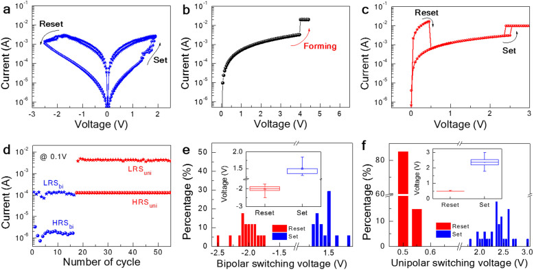
Figure 1 shows the schematic of the intended ReRAM device. All the detailed growth and fabrication processes are described in the method section below. Afterwards, this original SRO-SZO:Cr-Pt ReRAM device is called “M device”. Figures 2(a)–(c) show the measured RS I–V characteristics for this ReRAM device. The device first exhibited typical bipolar RS characteristics (Fig. 2(a)) with a counter clockwise (CCW) direction. The bistable reversible resistance states are controlled by the polarity of the applied bias voltage, as clearly understood from its name bipolar. However, as the bias voltage further increased in the low-resistance state, the resistance abruptly changed into a much lower resistance state (Fig. 2(b)). This process resembles soft dielectric breakdown, often referred to as “forming” in metal-insulator-metal ReRAM structures. Forming creates defect-induced local filamentary channels across a resistive insulator, and afterwards, unipolar RS controlled by the magnitude of the current (Fig. 2(c)) occurred, and the current compliance limit is needed to protect the device from the permanent dielectric breakdown. This change in the switching mode from bipolar to unipolar is irreversible and seems to be determined by the application of a high electric field across the ReRAM device, regardless of the switching cycle of the bipolar RS. Assuming that the forming voltage is larger than 4 V, the corresponding electric field across the SZO:Cr is of at least 6.7 × 10⁵ V/cm (4 V/60 nm). This field is comparable to that of bipolar RS ReRAM devices: 5 × 10⁵ V/cm (15 V/300 nm) for NiO, and 1 × 10⁶ V/cm (4 V/40 nm) for NbO26,27. To avoid any confusion, low and high resistance states for the bipolar RS mode are respectively abbreviated as LRSbi and HRSbi, and for the unipolar RS mode LRSuni and HRSuni are used. The switching process from LRS to the HRS and its inverse called ‘reset' and ‘set', respectively6. The HRS/LRS ratio at a read voltage (0.1 V) is of ~100 for the bipolar RS mode and of ~50 for the unipolar RS mode.
Figure 1. Resistive switching sample.
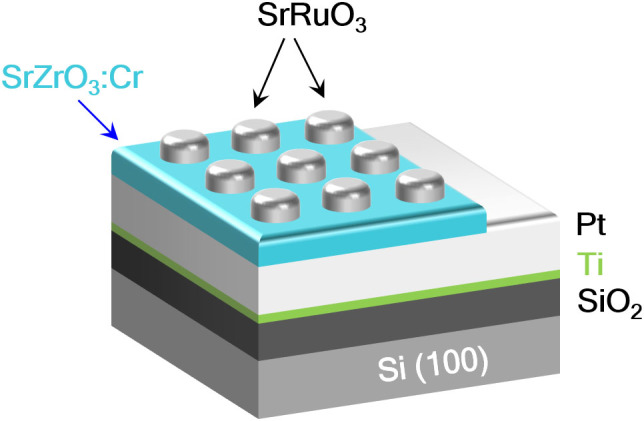
Schematic of the intended SRO/SZO:Cr/Pt/Ti/SiO2/Si device.
Figure 2. Electrical characterization of the fabricated resistive switching (RS) memory device.
Semi-log plot for the observed I–V curves of (a) the bipolar RS mode, (b) forming process, and (c) the unipolar RS mode after the forming process. (d) Endurance of the observed RS behavior at +0.1 V. Distributions of the measured switching voltages for (e) the bipolar and (f) unipolar RS mode. The insets in (e) and (f) present the average set and reset voltages.
The endurance test that plots the variation of the current at 0.1 V in each RS mode is shown in Fig. 2(d), demonstrating good switching reproducibility in each RS mode. We intentionally caused the bipolar → unipolar mode transformation after the 16th cycle of bipolar RS through the forming process. The RS cycle is counted consecutively, so the 17th cycle number corresponds to the first LRS in the unipolar RS mode. The LRSbi and HRSuni have similar resistances with in a tolerable range. This is because the LRSuni occurs in the LRSbi. One of the most interesting features is that although the current level of the LRSbi is very similar to that of the HRSuni, the stability of the HRSuni is much higher than that of the LRSbi, suggesting that the electrical nature of the conduction paths and the involved transport mechanisms are changed by the forming process. This is further clarified from temperature-dependent measurements of the electrical transport in each resistance state given below. The irreversibility of the unipolar mode into the bipolar mode suggests that the unipolar RS mechanism is completely different in many aspects.
The set and reset RS voltages for both the bipolar and unipolar modes are presented in Figs. 2(e) and (f), respectively. The reset voltage in the unipolar RS mode is very uniform compared to the other switching voltages. The insets show the averaged reset and set voltages in each switching mode. The observed uniform reset switching voltage in the unipolar mode indicates that conducting paths in every set switching cycle are reconstructed with similar properties. If we attribute the observed unipolar RS to the repeated process of the rupture/re-creation of filamentary channels, the conducting filaments with similar physical and chemical properties are created in each cycle. A detailed discussion of this issue will be given later together with the analysis on the compositional and structural properties of the device.
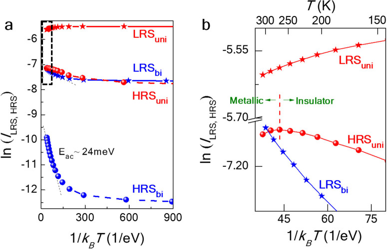
The nature of the electrical transport in each resistance state can be revealed by measuring its temperature dependence. Fig. 3(a) summarizes the measured temperature dependencies of the current at +0.1 V in each resistance state, plotting ln(I) against 1/kBT where kB and T represent the Boltzmann constant and the temperature, respectively. In order to maintain the conduction channel and transport mechanism unchanged during measurements, the temperature dependencies of the LRS and HRS states were measured separately at a low voltage of 0.1 V without repetition of LRS↔HRS switching at each temperature.
Figure 3. Temperature dependent resistive switching transport.
(a) Temperature dependent transport measurements of each resistance state and (b) enlarged graph dash-boxed in (a). Different temperature behaviors in each resistance state are indicative of different transport mechanisms. More detailed description is given in the text.
Since the change in the switching mode is irreversible, the temperature dependences of the LRSbi and HRSbi currents were first measured. The detailed transport mechanisms in each resistance state cannot be completely understood from the ln(I) vs. 1/kBT curves only. It was most apparent that whereas LRSuni shows metallic transport characteristics, HRSbi has insulator properties with a thermal activation energy of ~24 meV. The nature of the leakage transport in SZO can be described by a complex mixture of several possible conduction mechanisms. Reasonably satisfactory fits to the HRSbi I–V curves are achieved with the Frenkel-Poole model which describes field enhanced thermal excitation of trapped electrons into the conduction band in the low field region28,29. The observed low-field activation energy of the HRSbi is related with this process. Another interesting feature is that even though the current level is almost similar, HRSuni and LRSbi show different conduction behaviors with decreasing temperature. The dashed box in Fig. 3(a) is enlarged in Fig. 3(b). In the high temperature region, the thermionic emission feature of the LRSbi is much stronger than that of the HRSuni, even showing metallic transport similar to that of LRSuni. The metallic transport in the HRSuni at high temperatures is understood in terms of weak filamentary channels26. This weak filamentary conduction competes with existing conductions in the HRSuni, showing different thermal activation behaviors with decreasing temperature. Because metallic conduction through weak filamentary channels becomes stronger with increasing temperature, its thermal activation behavior becomes more clearly visible as observed in Fig. 3(b).
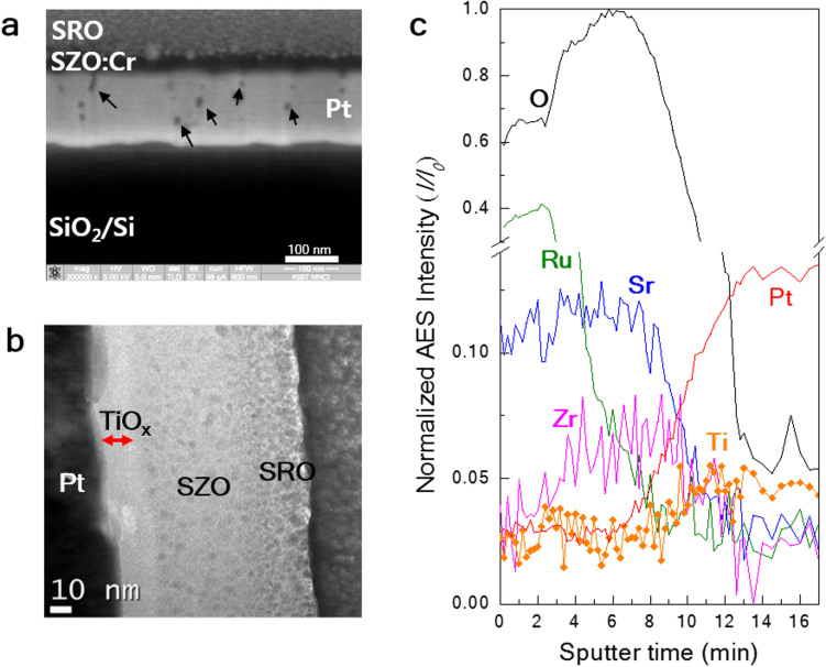
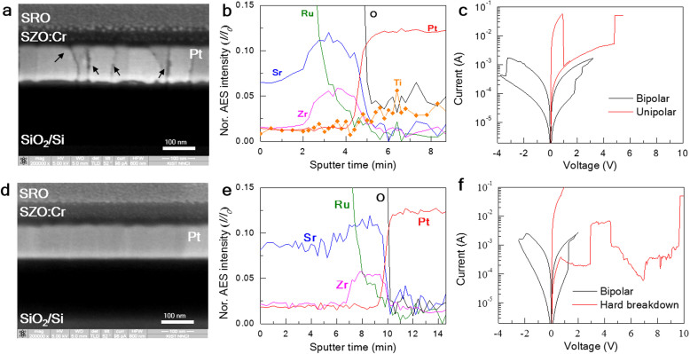
In order to figure out the origin of the observed irreversible RS mode transformation, we investigated the structural and compositional properties of the ReRAM device. Figure 4(a) shows the cross-sectional scanning electron microscope (SEM) image of the ReRAM device. Well-defined uniform layers are clearly observed with the intended thicknesses and are identified. However, dark spots embedded in the Pt electrode are also observed. These dark regions in the Pt layer indicate that it is relatively nonconductive. Furthermore, at the SZO:Cr/Pt interface, a thin unintended layer seems to be formed with a similar brightness as that of the dark spots. According to in-situ EDAX depth profiles (Figure S1 in the supporting information), the dark regions embedded in the Pt layer and at the SZO:Cr/Pt interface consist of mainly Ti and O.
Figure 4. Structural analyses of M device.
(a) SEM image of the device. Traces of relatively nonconductive spots are observed (marked with arrows). (b) TEM image of the device. A thin unintended TiOx layer is observed between the SZO:Cr and Pt layers. (c) Normalized AES depth profile for the device.
To more clearly confirm the layer configuration of the ReRAM device, transmission electron microscope (TEM) measurements were carried out, as shown in Fig. 4(b). The central SZO:Cr layer sandwiched by the Pt and SRO electrodes is clearly identified. We also detected a thin TiOx layer between the Pt electrode and the SZO:Cr layer. A continuum TiOx layer with non-uniform thickness is detected between the Pt and SZO:Cr layers. However, note that the structural nature of TiOx at the SZO:Cr/Pt interface depends on substrate temperature and growth time.
To conclusively find the elemental composition in of each layer, AES depth-profile measurements were also performed. Figure 4(c) shows the AES intensities for various elements as a function of the sputter time. Sharp boundaries between the intended layers are not obvious, and instead Sr, Zr and Ru, the main constituting elements, seem to inter-penetrate across the SRO/SZO boundary. Ti and Pt are also detected in the SZO region, and oxygen is omnipresent through the entire structure. The presence of Ti and O in the Pt layer indicates that the dark regions in the SEM image are due to the insulating properties of TiOx. Since Ti was not co-deposited together with the other elements, the source of Ti is certainly the Ti adhesion layer between Pt and SiO2. It was reported that a Ti adhesion layer out-diffuses through a Pt electrode at high enough substrate temperatures forming Pt-Ti compounds30. However, in the presence of oxygen, Ti can also form more complex compounds24,30,31.
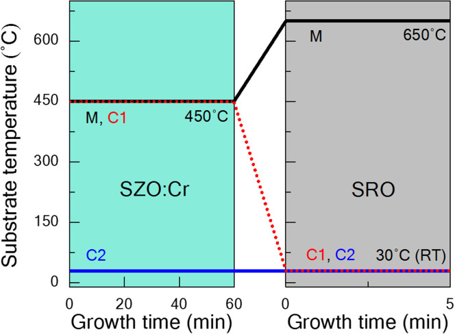
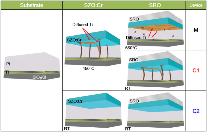
Two different SZO:Cr/SRO ReRAM devices, C1 and C2, were fabricated and compared to explicitly confirm the effects of the Ti adhesion layer out-diffusion on the structural properties and RS characteristics of the devices. SEM, depth-profile AES, and RS measurements were taken, and three devices of each were fabricated under the same fabrication conditions except for the substrate temperature. The substrate temperatures for the SZO and SRO layers of the ReRAM devices are schematically described in Fig. 5.
Figure 5. Substrate temperature during film's growth for the M, C1 and C2 devices.
For the M and C1 devices, after completing the SZO:Cr growth, the substrate temperature was reduced at a rate of 18 °C/min to RT at the base pressure.
Figure 6 shows a comparison of the cross-sectional SEM images and AES depth profiles of the prepared devices. For the C1 device, the SZO:Cr and SRO layers were deposited at 450 °C and at room temperature, respectively. The Ti adhesion layer out-diffusion is clearly visible through the Pt layer forming TiOx. However, compared to the main device (M device) where the SRO layer is deposited at 650 °C, it is obvious that Ti out-diffusion in the C1 device is actively under progress (compare the SEM images in Figs. 4 and 6). The corresponding AES depth-profile confirms the formation of TiOx in the Pt layer. This C1 device shows CCW bipolar RS characteristics, and the RS mode transformation occurred at ~5 V. However, for the C2 device, where both the SZO:Cr and SRO layers are deposited at room temperature, Ti adhesion layer out-diffusion does not occur. This is confirmed by the absence of Ti element in the corresponding AES depth profile. For this C2 device, although we observed similar CCW bipolar RS characteristics, permanent dielectric breakdown occurred at a much higher voltage instead of the forming process, and unipolar RS was not observed (in other words, no RS mode transformation occurred).
Figure 6. Structural analyses of C1 and C2 devices.
(a) SEM image of the C1 device. Traces of out-diffused Ti are observed as a linear form. (b) AES depth profile for the C1 device. Ti is detected at the SZO:Cr/Pt interface. (c) Resistive switching I–V curves for the C1 device showing RS transformation at ~5 V. (d) SEM image of the C2 device. Any trace of out-diffusion is not founded. (e) AES depth profile for the C2 device. Ti is not detected. (f) I–V curves for the C2 device. Hard dielectric breakdown occurred instead of an RS transformation.
Discussion
A schematic model of the Ti out-diffusion is illustrated in Fig. 7. For the bare Pt/Ti/SiO2/Si substrate, Ti out-diffusion through the Pt layer is not detected because the Pt layer was deposited at room temperature. This is confirmed by the cross-sectional SEM image shown in Fig. 6(b). During the deposition of the SZO:Cr and SRO layers at high substrate temperatures, Ti out-diffuses through the Pt layer, forming TiOx. If the substrate is heated long enough, a thin TiOx layer is formed between the Pt and SZO:Cr layers, as demonstrated in the TEM image in Fig. 4. Considering that the AES data shows a rapid decrease in the Ti intensity in the SZO region, Ti seems to not effectively out-diffuse through the SZO layer30. However, the out-diffused Ti in the SZO:Cr layer works as metallic defects, playing an important role in creating filamentary channels.
Figure 7. Schematics of Ti out-diffusion in sequence.
Depending on the substrate temperature, the Ti adhesion layer out-diffuses forming Ti compounds inside the Pt layer. RT: room temperature.
The schematic RS mechanisms in each RS mode are illustrated in Fig. 8. The RS mechanism for bipolar RS in perovskite hetero-junctions devices, including SZO:Cr/SRO systems, is well understood in terms of the redox chemical process at the interface15,32. It is found that bipolar resistive switching properties of SZO:Cr are strongly dependent on the configuration of electrodes used15. This implies that the redox chemical reaction at the interface plays a key role in determining the observed bipolar resistive switching. The low-field electrical transport through the SZO:Cr layer in the LRSbi is described by thermally activated hopping conduction channels via defects states28,29. The channels are depicted with thin broken lines in Fig. 8. Thus it is reasonable to describe the observed bipolar resistive switching transport in terms of the combined effects of the redox chemical reaction at the interface and thermally activated hopping conduction channels. A positive voltage bias on the top SRO electrode leads to oxygen-ions migration at the SRO/SZO:Cr interface, generating oxygen vacancies which are related to electron-hopping paths through in the SZO:Cr film (LRSbi). When a negative voltage bias is applied, the oxygen ions regenerates with the oxygen vacancies, and this process blocks the electron hopping paths (HRSbi).
Figure 8. Schematics of bipolar and unipolar mode RS mechanisms.
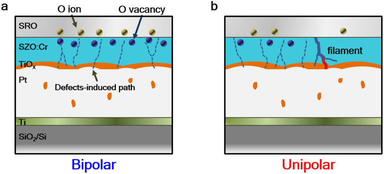
(a) Schematic of bipolar mode RS mechanism. Redox chemical reaction between oxygen vacancies and ions in the vicinity of the SRO/SZO:Cr interface plays a key role in determining the observed RS properties in case of bipolar RS mode. (b) Schematic of unipolar mode RS mechanism for the M and C1 devices where Ti out-diffusion occurs. After the electro-forming process, metallic filaments are created in the SZO:Cr layer. The observed unipolar resistive switching is caused by the repetition process of the rupture/re-creation of metallic filaments. Out-diffused Ti in the SZO:Cr contributes to the formation of metallic filaments.
Regardless of the presence of the Ti out-diffusion-induced TiOx layer between Pt and SZO:Cr, the three ReRAM devices showed similar bipolar RS characteristics. This implies that the TiOx layer does not play a key role in determining the initial bipolar RS mode. However, if a high enough dielectric breakdown voltage is applied across the devices, the situation becomes different. Only the device (C2) without Ti out-diffusion shows permanent dielectric breakdown without RS mode transformation from bipolar into unipolar mode. Since Ti is chemically active with nearby oxygen, we propose that out-diffused Ti provides a suitable circumstance for the formation of metallic conducting filaments across the SZO:Cr layer. The role of out-diffused Ti in the observed unipolar RS characteristics is similar to that of additional metal doping in RS oxide materials13,17,33.
Analyses of the Ti out-diffusion induced TiOx layer in the RS mode transformation and RS properties reveals that its presence does not affect the initial bipolar RS characteristics. However, the lower forming voltages for the M and C1 devices including a TiOx layer were observed than the dielectric breakdown voltage for the C2 device without having a TiOx layer (Figure S2 in the supporting information). In addition, the forming voltage of the M device with a relatively thicker TiOx layer, was smaller than that of the C1 device. This suggests that the presence of the TiOx layer affects the forming process.
In conclusion, we fabricated SrRuO3/SrZrO3:Cr hetero-junction ReRAM structures on Pt/Ti/SiO2 substrates at different substrate temperatures and investigated their resistive switching characteristics. We observed bipolar-type reversible resistive switching in the low voltage region below ±3 V. However, as the voltage is increased, an irreversible RS mode transformation from bipolar to unipolar mode occurred. We found that unintentional Ti atom out-diffusion at high substrate temperatures plays a key role in determining the irreversible RS mode transformation. The diffused Ti atoms in the SZO:Cr layer are also expected to contribute to the leakage current and forming voltage. We attribute the observed bipolar and unipolar RS characteristics to redox chemical interaction at the SRO-SZO:Cr interfacial region and Ti atom out-diffusion-assisted metallic filaments across the SZO:Cr layer, respectively. Our experimental findings and analysis clearly demonstrate that metal out-diffusion phenomena can influence resistive switching characteristics in typical metal-insulator-metal structures. From the viewpoint of technology, the substrate temperature-induced metal out-diffusion effect could provide a novel way to fabricate ReRAM devices improving their resistive switching performance.
Methods
An SrRuO3/SrZrO3:Cr/Pt capacitor structure was fabricated as a practical application of the resistive switching characteristics in nonvolatile memories. The intended ReRAM device structure consists of a 80-nm-thick 0.2 at.% Cr-doped (i.e., 3 × 10¹⁹ atoms/cm3) SrZrO3 (SZO:Cr) film grown on Pt(111)/Ti/SiO2/Si(100) substrates via radio frequency reactive magnetron sputtering deposition at a substrate temperature of 450°C. The 90° off-axis method was employed to decrease plasma damage on the film's surface. A few-nm-thick Ti layer was pre-deposited as an adhesion layer between the bottom Pt electrode and the SiO2 layer. Before deposition, the base pressure of the chamber was kept at 5 × 10⁻⁷ Torr. During the deposition, the argon working pressure and the rotation speed of the substrate holder were set to 50 mTorr and 3 rpm, respectively. The oxygen content was fixed at 10%. For the transport measurements, 300 nm thick SrRuO3 (SRO) top electrodes with a diameter of 300 μm were patterned on the SZO:Cr layer via focused magnetron sputtering with a tungsten shadow mask at a substrate temperature of 650 °C. A schematic diagram of the intended device structure is shown in Fig. 1. Another two different ReRAM devices were fabricated under the same fabrication conditions except for the substrate temperature during the deposition of the SZO:Cr and SRO layers to perform an experimental demonstration of the effect of the metal adhesion out-diffusion had on resistive switching.
Compositional analyses of the devices were performed using the depth profile of Auger electron spectroscopy (AES). Conventional two-terminal resistance switching current-voltage (I–V) measurements were carried out using a parameter analyzer over the temperature range between 300 K and 10 K, in voltage sweep mode. For the resistive switching measurements, we applied a bias voltage to the top electrode, with the bottom electrode grounded.
Author Contributions
H.I. designed this work and prepared the manuscript. The experimental and electrical measurements were carried out by Y.J., K.J., J.K., H.W., J.H. and H.K. J.H. and J.-K.L. have analyzed the results and discussed the manuscript during the preparation. All authors discussed the results and implications and commented on the manuscript at all stages.
Supplementary Material
Supplementary Information
Acknowledgments
This project was supported by the National Research Foundation (NRF) of Korea (Grant No. 2013-044975) and by KIST program (2E24871). This work was also supported partly by the R&D Program of the Ministry of Knowledge Economy of the Republic of Korea [KI10039191, Development of Fundamental Technologies for Terabit-Level 3D ReRAM].
References
- Waser R. et al. Redox-Based resistive switching memories – nanoionic mechanisms, prospects, and challenges. Adv. Mater. 21, 2632–2663 (2009). [DOI] [PubMed] [Google Scholar]
- Moreno C. et al. Reversible resistive switching and multilevel recording in La0.7Sr0.3MnO3 thin films for low cost nonvolatile memories. Nano Lett. 10, 3828–3835 (2010). [DOI] [PubMed] [Google Scholar]
- Zhao L. et al. Multi-level control of conductive nano-filament evolution in HfO2 ReRAM by pulse-train operations. Nanoscale 6, 5698–702 (2014). [DOI] [PubMed] [Google Scholar]
- Jo Y. et al. Multi-valued resistive switching characteristics in WOx/AlOy heterojunction resistive switching memories. J. Korean Phys. Soc. 64, L173–L176 (2014). [Google Scholar]
- Nagashima K. et al. Resistive switching multistate nonvolatile memory effects in a single cobalt oxide nanowire. Nano lett. 10, 1359–1363 (2010). [DOI] [PubMed] [Google Scholar]
- Sawa A. Resistive switching in transition metal oxides. Mater. Today 11, 28–36 (2008). [Google Scholar]
- Hickmott T. W. Low-frequency negative resistance in thin anodic oxide films. J. Appl. Phys. 33, 2669–2682 (1962). [Google Scholar]
- Lee S. B. et al. Scaling behaviors of reset voltages and currents in unipolar resistance switching. Appl. Phys. Lett. 93, 212105 (2008). [Google Scholar]
- Chen J. et al. Dynamic evolution of conducting nanofilament in resistive switching memories. Nano Lett. 13, 3671–3677 (2013). [DOI] [PubMed] [Google Scholar]
- Kim K. M. et al. Collective motion of conducting filaments in Pt/n-Type TiO2/p-Type NiO/Pt stacked resistance switching memory. Adv. Funct. Mater. 21, 1587–1592 (2011). [Google Scholar]
- Chang S. H. et al. Occurrence of both unipolar memory and threshold resistance switching in a NiO film. Phys. Rev. Lett. 102, 026801 (2009). [DOI] [PubMed] [Google Scholar]
- Jung K. et al. Unipolar resistive switching in insulating niobium oxide film and probing electroforming induced metallic components. J. Appl. Phys. 109, 054511 (2011). [Google Scholar]
- Jung K. et al. Resistance switching characteristics in Li-doped NiO. J. Appl. Phys. 103, 034504 (2008). [Google Scholar]
- Janousch M. et al. Role of oxygen vacancies in Cr-doped SrTiO3 for resistance-change memory. Adv. Mater. 19, 2232–2235 (2007). [Google Scholar]
- Park J. et al. Electrode dependence of bipolar resistive switching in SrZrO3:Cr perovskite film-based memory devices. Electrochem. Solid-State Lett. 11, H226–H229 (2008). [Google Scholar]
- Asamitsu A. et al. Current switching of resistive states in magnetoresistive manganites. Nature 388, 50–52 (1997). [Google Scholar]
- Choi J. et al. Bipolar resistance switching characteristics in a thin Ti–Ni–O compound film. Nanotechnology 20, 175704 (2009). [DOI] [PubMed] [Google Scholar]
- Jo Y. et al. Tailoring resistive switching characteristics in WOx films using different metal electrodes. Curr. Appl. Phys. 14, S93–S97 (2014). [Google Scholar]
- Shibuya K. et al. Impact of defect distribution on resistive switching characteristics of Sr2TiO4 thin films. Adv. Mater. 22, 411–414 (2010). [DOI] [PubMed] [Google Scholar]
- Kwak J. S. et al. Roles of interfacial TiOxN1−x layer and TiN electrode on bipolar resistive switching in TiN/TiO2 /TiN frameworks. Appl. Phys. Lett. 96, 223502 (2010). [Google Scholar]
- Bae Y. C. et al. Oxygen ion drift-induced complementary resistive switching in homo TiOx/TiOy/TiOx and hetero TiOx/TiON/TiOx triple multilayer frameworks. Adv. Funct. Mater. 22, 709–716 (2012). [Google Scholar]
- Tang M. H. et al. Bipolar and unipolar resistive switching behaviors of sol–gel-derived SrTiO3 thin films with different compliance currents. Semicond. Sci. Technol. 26, 075019 (2011). [Google Scholar]
- Sun X. et al. Coexistence of the bipolar and unipolar resistive switching behaviours in Au/SrTiO3/Pt cells. J. Phys. D: Appl. Phys. 44, 125404 (2011). [Google Scholar]
- Yang J. J. et al. Diffusion of adhesion layer metals controls nanoscale memristive switching. Adv. Mater. 22, 4034–4038 (2010). [DOI] [PubMed] [Google Scholar]
- Shuai Y. et al. Key concepts behind forming-free resistive switching incorporated with rectifying transport properties. Sci. Rep. 3, 02208 (2013). [DOI] [PMC free article] [PubMed] [Google Scholar]
- Jung K. et al. Temperature dependence of high- and low-resistance bistable states in polycrystalline NiO films. Appl. Phys. Lett. 90, 052104 (2007). [Google Scholar]
- Jung K. et al. Electrically induced conducting nanochannels in an amorphous resistive switching niobium oxide film. Appl. Phys. Lett. 97, 233509 (2010). [Google Scholar]
- Rossel C. et al. Electrical current distribution across a metal-insulator-metal structure during bistable switching. J. Appl. Phys. 90, 2892–2898 (2001). [Google Scholar]
- Yoon J. H. et al. Highly uniform, electroforming-free, and self-rectifying resistive memory in the Pt/Ta2O5/HfO2-x/TiN structure. Adv. Funct. Mater. 24, 5086–5095 (2014). [Google Scholar]
- Park K. H. et al. Microstructures and interdiffusions of Pt/Ti electrodes with respect to annealing in the oxygen ambient. J. Mater. Res. 10, 1790–1794 (1995). [Google Scholar]
- Goux L. et al. Role of Ti out-diffusion from a Pt/Ti bi-layer on the crystalline growth of (Ba,Sr)TiO3: A transmission electron microscopy investigation. Thin Solid Films 515, 1260–1265 (2006). [Google Scholar]
- Beck A. et al. Reproducible switching effect in thin oxide films for memory applications. Appl. Phys. Lett. 77, 139–141 (2000). [Google Scholar]
- Do Y. H. et al. Nonvolatile unipolar and bipolar resistive switching characteristics in Co-doped TiO2 thin films with different compliance currents. J. Korean Phys. Soc. 55, 1009–1012 (2009). [Google Scholar]
Associated Data
This section collects any data citations, data availability statements, or supplementary materials included in this article.
Supplementary Materials
Supplementary Information


